EP0138332A1 - Méthodes d'utilisation de l'excitation optique sélective lors de procédés de dépôt et la détection de nouveaux composés - Google Patents
Méthodes d'utilisation de l'excitation optique sélective lors de procédés de dépôt et la détection de nouveaux composés Download PDFInfo
- Publication number
- EP0138332A1 EP0138332A1 EP84305612A EP84305612A EP0138332A1 EP 0138332 A1 EP0138332 A1 EP 0138332A1 EP 84305612 A EP84305612 A EP 84305612A EP 84305612 A EP84305612 A EP 84305612A EP 0138332 A1 EP0138332 A1 EP 0138332A1
- Authority
- EP
- European Patent Office
- Prior art keywords
- species
- sih
- deposition
- reaction
- deposition reaction
- Prior art date
- Legal status (The legal status is an assumption and is not a legal conclusion. Google has not performed a legal analysis and makes no representation as to the accuracy of the status listed.)
- Withdrawn
Links
Images




Classifications
-
- C—CHEMISTRY; METALLURGY
- C23—COATING METALLIC MATERIAL; COATING MATERIAL WITH METALLIC MATERIAL; CHEMICAL SURFACE TREATMENT; DIFFUSION TREATMENT OF METALLIC MATERIAL; COATING BY VACUUM EVAPORATION, BY SPUTTERING, BY ION IMPLANTATION OR BY CHEMICAL VAPOUR DEPOSITION, IN GENERAL; INHIBITING CORROSION OF METALLIC MATERIAL OR INCRUSTATION IN GENERAL
- C23C—COATING METALLIC MATERIAL; COATING MATERIAL WITH METALLIC MATERIAL; SURFACE TREATMENT OF METALLIC MATERIAL BY DIFFUSION INTO THE SURFACE, BY CHEMICAL CONVERSION OR SUBSTITUTION; COATING BY VACUUM EVAPORATION, BY SPUTTERING, BY ION IMPLANTATION OR BY CHEMICAL VAPOUR DEPOSITION, IN GENERAL
- C23C16/00—Chemical coating by decomposition of gaseous compounds, without leaving reaction products of surface material in the coating, i.e. chemical vapour deposition [CVD] processes
- C23C16/44—Chemical coating by decomposition of gaseous compounds, without leaving reaction products of surface material in the coating, i.e. chemical vapour deposition [CVD] processes characterised by the method of coating
- C23C16/52—Controlling or regulating the coating process
-
- B—PERFORMING OPERATIONS; TRANSPORTING
- B01—PHYSICAL OR CHEMICAL PROCESSES OR APPARATUS IN GENERAL
- B01J—CHEMICAL OR PHYSICAL PROCESSES, e.g. CATALYSIS OR COLLOID CHEMISTRY; THEIR RELEVANT APPARATUS
- B01J12/00—Chemical processes in general for reacting gaseous media with gaseous media; Apparatus specially adapted therefor
- B01J12/002—Chemical processes in general for reacting gaseous media with gaseous media; Apparatus specially adapted therefor carried out in the plasma state
-
- B—PERFORMING OPERATIONS; TRANSPORTING
- B01—PHYSICAL OR CHEMICAL PROCESSES OR APPARATUS IN GENERAL
- B01J—CHEMICAL OR PHYSICAL PROCESSES, e.g. CATALYSIS OR COLLOID CHEMISTRY; THEIR RELEVANT APPARATUS
- B01J19/00—Chemical, physical or physico-chemical processes in general; Their relevant apparatus
- B01J19/08—Processes employing the direct application of electric or wave energy, or particle radiation; Apparatus therefor
- B01J19/12—Processes employing the direct application of electric or wave energy, or particle radiation; Apparatus therefor employing electromagnetic waves
- B01J19/121—Coherent waves, e.g. laser beams
-
- C—CHEMISTRY; METALLURGY
- C01—INORGANIC CHEMISTRY
- C01B—NON-METALLIC ELEMENTS; COMPOUNDS THEREOF; METALLOIDS OR COMPOUNDS THEREOF NOT COVERED BY SUBCLASS C01C
- C01B33/00—Silicon; Compounds thereof
- C01B33/08—Compounds containing halogen
- C01B33/107—Halogenated silanes
-
- C—CHEMISTRY; METALLURGY
- C01—INORGANIC CHEMISTRY
- C01G—COMPOUNDS CONTAINING METALS NOT COVERED BY SUBCLASSES C01D OR C01F
- C01G17/00—Compounds of germanium
- C01G17/04—Halides of germanium
-
- C—CHEMISTRY; METALLURGY
- C23—COATING METALLIC MATERIAL; COATING MATERIAL WITH METALLIC MATERIAL; CHEMICAL SURFACE TREATMENT; DIFFUSION TREATMENT OF METALLIC MATERIAL; COATING BY VACUUM EVAPORATION, BY SPUTTERING, BY ION IMPLANTATION OR BY CHEMICAL VAPOUR DEPOSITION, IN GENERAL; INHIBITING CORROSION OF METALLIC MATERIAL OR INCRUSTATION IN GENERAL
- C23C—COATING METALLIC MATERIAL; COATING MATERIAL WITH METALLIC MATERIAL; SURFACE TREATMENT OF METALLIC MATERIAL BY DIFFUSION INTO THE SURFACE, BY CHEMICAL CONVERSION OR SUBSTITUTION; COATING BY VACUUM EVAPORATION, BY SPUTTERING, BY ION IMPLANTATION OR BY CHEMICAL VAPOUR DEPOSITION, IN GENERAL
- C23C16/00—Chemical coating by decomposition of gaseous compounds, without leaving reaction products of surface material in the coating, i.e. chemical vapour deposition [CVD] processes
- C23C16/22—Chemical coating by decomposition of gaseous compounds, without leaving reaction products of surface material in the coating, i.e. chemical vapour deposition [CVD] processes characterised by the deposition of inorganic material, other than metallic material
- C23C16/24—Deposition of silicon only
-
- C—CHEMISTRY; METALLURGY
- C23—COATING METALLIC MATERIAL; COATING MATERIAL WITH METALLIC MATERIAL; CHEMICAL SURFACE TREATMENT; DIFFUSION TREATMENT OF METALLIC MATERIAL; COATING BY VACUUM EVAPORATION, BY SPUTTERING, BY ION IMPLANTATION OR BY CHEMICAL VAPOUR DEPOSITION, IN GENERAL; INHIBITING CORROSION OF METALLIC MATERIAL OR INCRUSTATION IN GENERAL
- C23C—COATING METALLIC MATERIAL; COATING MATERIAL WITH METALLIC MATERIAL; SURFACE TREATMENT OF METALLIC MATERIAL BY DIFFUSION INTO THE SURFACE, BY CHEMICAL CONVERSION OR SUBSTITUTION; COATING BY VACUUM EVAPORATION, BY SPUTTERING, BY ION IMPLANTATION OR BY CHEMICAL VAPOUR DEPOSITION, IN GENERAL
- C23C16/00—Chemical coating by decomposition of gaseous compounds, without leaving reaction products of surface material in the coating, i.e. chemical vapour deposition [CVD] processes
- C23C16/44—Chemical coating by decomposition of gaseous compounds, without leaving reaction products of surface material in the coating, i.e. chemical vapour deposition [CVD] processes characterised by the method of coating
- C23C16/48—Chemical coating by decomposition of gaseous compounds, without leaving reaction products of surface material in the coating, i.e. chemical vapour deposition [CVD] processes characterised by the method of coating by irradiation, e.g. photolysis, radiolysis, particle radiation
- C23C16/483—Chemical coating by decomposition of gaseous compounds, without leaving reaction products of surface material in the coating, i.e. chemical vapour deposition [CVD] processes characterised by the method of coating by irradiation, e.g. photolysis, radiolysis, particle radiation using coherent light, UV to IR, e.g. lasers
-
- C—CHEMISTRY; METALLURGY
- C23—COATING METALLIC MATERIAL; COATING MATERIAL WITH METALLIC MATERIAL; CHEMICAL SURFACE TREATMENT; DIFFUSION TREATMENT OF METALLIC MATERIAL; COATING BY VACUUM EVAPORATION, BY SPUTTERING, BY ION IMPLANTATION OR BY CHEMICAL VAPOUR DEPOSITION, IN GENERAL; INHIBITING CORROSION OF METALLIC MATERIAL OR INCRUSTATION IN GENERAL
- C23C—COATING METALLIC MATERIAL; COATING MATERIAL WITH METALLIC MATERIAL; SURFACE TREATMENT OF METALLIC MATERIAL BY DIFFUSION INTO THE SURFACE, BY CHEMICAL CONVERSION OR SUBSTITUTION; COATING BY VACUUM EVAPORATION, BY SPUTTERING, BY ION IMPLANTATION OR BY CHEMICAL VAPOUR DEPOSITION, IN GENERAL
- C23C16/00—Chemical coating by decomposition of gaseous compounds, without leaving reaction products of surface material in the coating, i.e. chemical vapour deposition [CVD] processes
- C23C16/44—Chemical coating by decomposition of gaseous compounds, without leaving reaction products of surface material in the coating, i.e. chemical vapour deposition [CVD] processes characterised by the method of coating
- C23C16/48—Chemical coating by decomposition of gaseous compounds, without leaving reaction products of surface material in the coating, i.e. chemical vapour deposition [CVD] processes characterised by the method of coating by irradiation, e.g. photolysis, radiolysis, particle radiation
- C23C16/488—Protection of windows for introduction of radiation into the coating chamber
-
- G—PHYSICS
- G01—MEASURING; TESTING
- G01N—INVESTIGATING OR ANALYSING MATERIALS BY DETERMINING THEIR CHEMICAL OR PHYSICAL PROPERTIES
- G01N21/00—Investigating or analysing materials by the use of optical means, i.e. using sub-millimetre waves, infrared, visible or ultraviolet light
- G01N21/62—Systems in which the material investigated is excited whereby it emits light or causes a change in wavelength of the incident light
- G01N21/63—Systems in which the material investigated is excited whereby it emits light or causes a change in wavelength of the incident light optically excited
- G01N21/64—Fluorescence; Phosphorescence
- G01N21/6402—Atomic fluorescence; Laser induced fluorescence
Definitions
- This invention relates generally to the use of optical excitation, particularly induced by a tunable laser, for the detection of new compositions and improved methods of depositing a material like a photoconductive film on a substrate.
- optical absorption and emission spectroscopy are optical absorption and emission spectroscopy.
- Optical absorption spectroscopy lacks spacial resolution in three dimensions and is much less sensitive than laser-induced fluorescence, precluding its use for the detection of species present in low concentrations or in the vicinity of the important gas- surface interface region.
- Emission spectroscopy by its very nature can only detect species that are in vibrationally or electronically excited states. The concentrations of species in the ground state far exceed those in the excited state and thus the method becomes effective only in monitoring a small fraction of the transient species present in the deposition process. Also, the excitation rate from the ground state to the observed excited state is often unknown and may depend on external parameters such as gas pressure and flow rate.
- Another limitation of these analytical techniques is that they do not provide a non-perturbing pinpoint probe that can accurately measure low, i.e. sub-Torr, concentrations of highly reactive chemical species in the presence of rapidly changing chemical and temperature fields.
- transient atomic and molecular species are produced in chemical vapor deposition, diffusion flame, and glow-discharge reactors by pyrolysis, chemical reactions, or electron bombardment. Some of these species may play a prominent role in the deposition of the film itself. Monitoring their concentrations accurately and with a nondestructive analytical technique would be very helpful in un- derstaading the fabrication of the films. It is even more difficult to monitor the existence of transient species which may affect the quality of the film or coating being deposited if the species itself is not optically emitting or its emissions are not resolvable by the techniques described above.
- photovoltaic quality films of amorphous SiH x Fy prepared by the plasma-induced reaction of, for example, SiF 4 and I1 2 appear to contain unusual bonding configurations involving the intimate association of silicon with both fluorine and hydrogen atoms.
- the creation of radical sub-fluorides of silicon has been suggested as a mechanism for the deposition of such films.
- the presence of various excited-state neutral silicon radical species, i.e. SiF, SiH, SiF3, and Si has been demonstrated through the use of optical emission techniques in diffusion flames.
- Other radicals, especially in the ground state, have escaped detection and thus have hindered analysis of the effect these radical species have on the quality of the deposited film.
- optically excited fluorescence emission induced, for example, by a high or low power laser is an analytical technique which directly measures the ground-state concentration of a particular species. Analysis of a reaction is advantageously used as a non-perturbative probe capable of pinpoint spatial accuracy.
- selective optical excitation induced, for example, by a relatively high power laser can be an advantageous modification technique for improving the quality of deposited film.
- a relatively high power laser can be used as a perturbative means for exciting a selected species to modify the deposition reaction.
- the depositing process can be accurately monitored and controlled to produce the desired film deposit.
- the present invention includes a gaseous composition having the formula SiHF. Also included is a composition containing the elements silicon, hydrogen, and fluorine which exhibits characteristic fluorescence emission at the following wavelengths expressed in nanometers: 430.0, 446.5, 464.5, 483.5, 503.5, and 548.9, as illustrated in Fig. 4. The composition also exhibits characteristic excitation at the following wavelengths expressed in nanometers: 430.0, 420.0, 410.5, 401.5, and 393.0, as illustrated in Fig. 2.
- the present invention also includes methods of detecting a species in a flow reacti.on occuring in either a plasma or a diffusion flame which includes the step of inducing the fluorescence of said species with a laser.
- Another method contemplated by the invention is for de positing a material on a substrate including the steps of inducing a deposition reaction having at least one reactant.
- the deposition reaction is in operative contact with a substrate so that the product of the deposition reaction is a body of material deposited on the substrate.
- the method further includes detecting a species in the deposition reaction and measuring the relative concentration of the species.
- Another step deposits the material on the sub strate.
- Another contemplated method deposits a photoconductive film by inducing a deposition reaction having at least one reactant.
- the deposition reaction is in operative contact with the substrate so that the product of the deposition re action is a photoconductive film deposited on the substrate.
- the method further includes detecting a transient species having a stable excited state by inducing the fluorescence of the species with an optical excitation source and measuring the relative concentration of the species.
- Another step deposits the photoconductive film on the substrate.
- a novel method of depositing an improved photoconduc- . tive film includes the step of inducing a deposition reaction in operative contact with a substrate so that the product of the deposition reaction is a photoconductive film deposited on the substrate.
- the deposition reaction is modified by exciting an effective concentration of a specie so that the deposited photoconductive film is modified.
- the species is a precursor to the deposited film.
- Another step deposits the photoconductive film on the substrate.
- the present invention also includes an apparatus for depositing material which includes a reactor for inducing a deposition reaction having at least one reactant.
- An optical excitation source is positioned for probing the reactor and a substrate is positioned in operative contact with the deposition reaction in the reactor.
- the apparatus includes means for detecting a species in the deposition reaction, inducing the fluorescence of the species with the optical excitation source, and measuring the relative concentration of the species.
- Another apparatus embodiment contemplated by the invention includes a reactor for inducing a deposition reaction.
- the deposition reaction includes a species which is a precursor to the material deposited as the product of the deposition reaction.
- a substrate is positioned in operative contact with the deposition reaction in the reactor.
- the apparatus includes means for exciting an effective concentration of the species to a stable excited state in order to perturb the deposition reaction by operative contact therewith and modify the deposited material.
- the invention also includes an improved photoconductive material and an improved photovoltaic device made from such a material.
- the photoconductive material is deposited while in operative contact with an effective concentration of a species for modifying said material.
- the species is a precursor to a material deposited as the product of a deposition reaction and is induced to a stable excited state during the deposition of the material.
- the present invention generally relates to the use of fluorescence signals obtained by selective optical excitation to detect and monitor a species present during a flow reaction or decomposition of various reactants. These reactions were analyzed in situ using a tunable laser as a selective excitation source in combination with a reactor inducing such reactions with a diffusion flame or plasma- The resultant spectra and analysis presented below demonstrates the detection of a species like SiHF in the gas phase.
- the invention allows for pinpoint spatial probing of the reactor without perturbing the reaction.
- a deposition process can be controlled by monitoring a selected species and adjusting the deposition reaction parameters in response to the species' mere detection or relative concentration.
- the invention also contemplates perturbing deposition reactions by selectively exciting a species present in the deposition reaction to modify the deposited material so that the quality of the.deposited material improves.
- a fluorescent species can be excited by electromagnetic radiation and, as a consequence, reemit radiation either of the same wavelength or of a modified wavelength. At least one of the excited states of a species should be attractive or stable, otherwise the species will dissociate upon excitation. An excited species can return to its ground state by any of several mechanistic paths; the favored route is the one that minimizes the lifetime of the excited state. Thus, if deactivation by fluorescence is rapid with respect to other processes such emission is observed. On the other hand, if a radiationless path has a more favorable rate con stant, fluorescence is either absent or less intense. Fluo rescence spectroscopy is most useful in analyzing systems incorporating structural and environmental features that cause the rate of radiationless relaxation or deactivation reactions to be slowed to a point where the emission reaction can compete kinetically.
- FIG. 1 A schematic of a laser-induced fluorescence apparatus 10 contemplated by the present invention is illustrated in Fig. 1.
- the reactant gases are introduced into the reactor 15 through two concentric glass tubings 20, 25 with 3mm dia meter tapered ends 30, 35.
- the ground-state radicals produced in the .reaction are excited by a PAR Dyescan 2100 pulsed tunable dye laser 40 which uses a pulse width of 5 ns. and a bandwidth 0.04 nm. in the region of 390-470 nm.
- the laser beam 45 enters the reactor 10 through a series of black baffles 50 designed to reduce scattered laser light.
- An excitation spectrum is obtained by focusing the fluorescence with an (f/4) lens system 55 onto a photomultiplier 61 with a EMI 9885A bialkali cathode (not shown), and the resulting signal is averaged by a PAR 165 boxcar 65.
- a trigger mechanism 70 connects the laser 40 to the boxcar 65.
- Time-resolved fluorescence decays are displayed on a recorder 75 with 2 ns. resolution by the boxcar 65.
- Other means for detecting a species in a deposition reaction, inducing fluorescence of the species and measuring the relative concentration of the species also are contemplated by the invention.
- Other selective optical excitation sources are suitable.
- the species SiHF (X l A') was produced in a flow reaction of silane with fluorine using a diffusion flame typically with a 4:1 mole ratio at a total pressure of 0.05-0.15 Torr and flow rates of 2-5 sccm.
- the fluorescence in much of the excitation region was sufficiently strong to allow a spectral resolution to be made.
- the laser 40 was first set at a predetermined frequency corresponding to a band head; the resulting fluorescence was then focused onto the entrance slit of a Plasmascan PSS-2M monochromator (not shown) having a resolution of 3.5 nm. usually scanned at 10-20 nm./min.
- the photomultiplier 60 attached to the exit slit senses the signal which is averaged by the boxcar 65 with a time constant of 100 us.
- Fig. 2 is a spectrum of fluorescence excitation obtained between 390 and 470 nm at laser power levels of 10-20 uJ/pulse produced during the above-identified reaction.
- the spectrum has been normalized for laser intensity and detector spectral response.
- SiF A 2 ⁇ + - X 2 H
- all the other intense bands are significantly broader and are shaded towards the ultraviolet region.
- This spectrum is remarkably similar in appearance to the chemiluminescence spectrum of SiHCl, reported in Conner et al., J. Amer. Chem. Soc.
- F ig. 4 is a spectrum of resolved fluorescence emission accompanying laser excitation at 430.0 and 446.5 nm. From the observed band spacings in these spectra, the bending frequency ⁇ 2 of the SiHF in the ground state is found to be roughly 860 cm- 1 , in excellent agreement with the value of 859 cm- 1 derived from a recent infra-red analysis of matrix- isolated SiHF, in ismail et al., J. Chem. Phys. 77 (1982) 1626.
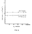
- T R for SiF and SiHF are found to be 255 + 10 ns. and 185+ 10 ns., respectively.
- TR value for SiF is 10-15% longer than that reported by Armstrong et al., J. Chem. Phys. 71 (1979) 2433, from their studies of this reaction. The discrepancy may be explained by the significantly higher pressure regimes (up to 10 Torr) under which Armstrong et al. performed their measurements.
- Fig. 6 is a spectrum of laser-induced fluorescence emission of the flow reaction of GeH 4 and fluorine run under the same conditions described above. The eight prominent peaks at 396.5, 402.8, 409.4, 416.3, 423.6, 431.1, 433.2, 443.7, and 449.2 nm. are assignable to GeF. The spectrum demonstrates the detection of transient species GeF and the usefulness of this invention for the detection of species other than those containing the silicon atom.
- Electrodes 80, 85 placed in a reactor 15 consists of two parallel 4 x 24 centimeter stainless steel plates, one of which is connected to a variable-frequency r.f. power supply 9.0 and matching network 92.
- the discharge is typically operated in the range of 100 KHz and at 10 W.
- the laser beam 40 was directed parallel to the electrodes 80, 85 and the fluorescence passes through a hole 95 of approximately 1 centimeter in diameter on the upper electrode 85.
- Suitable band-pass filters 100 were used to block out the discharge emission occurring outside' the region of interest which was predetermined to be 400-450 nm.
- Fig. 8 is a spectrum of-laser-induced fluorescence excitation detecting SiF in the discharge decomposition of SiF 4 at a pressure of 0.5 Torr. This illustrates the successful use of laser-induced fluorescence to the detection of chemical intermediates or transient species present in glow-discharge decomposition reactors. Although the laser-induced fluorescence signals in this spectra are far weaker than in the diffusion flame reaction, the SiF species shows up clearly in the excitation spectrum as assigned therein. Analysis of these laser-induced fluorescence spectra indicates a vibrational temperature of about 700-900 K for the SiF product.
- the present invention includes methods for depositing a material on a substrate. These methods induce a deposition reaction having at least one reactant.
- the deposition reaction may use a diffusion flame, or preferably, a plasma such as created by a glow discharge.
- the deposition reaction is positioned in operative contact with a substrate so that the product of the deposition reaction is a body of material deposited on the substrate.
- Preferred reactants used in a diffusion flame deposition reaction includes a mixture of fluorine or fluorine containing compounds with at least one of the following reactants: SiH 4 , SiH 3 F, SiH 2 F 2 , GeH 4 , GeH 3 F, and GeH 2 F 2 . More than one of these reactants may be combined in the mixture.
- Other reactants which include atoms of silicon or germanium are suitable.
- Preferred reactants used in a plasma deposition reaction includes at least one of the following reactants: SiH 4 , SiH 3 F, SiH 2 F 2 , SiHF 3 , SiF 4 , GeH 4 , GeH 3 F, GeH 2 F 2 , GeHF 3 , and GeF 4 . More than one of these reactants may be combined in a mixture. These reactants also may be used singly, or in combination, with hydrogen. Other reactants which include atoms of silicon or germanium are suitable.
- the method also includes detecting a species in the deposition reaction.
- the species has at least one attractive or stable excited state.
- the formula for the species is preferably SiH 2 , SiH, SiHF, SiF, SiF 2 , GeH 2 , GeH, GeHF, GeF, and GeF 2 .
- Other suitable species include either silicon or germanium atoms. Not only is the mere presence of a particular species detected, but its concentration relative to the other species present may be measured.
- the detecting step further includes inducing fluorescence of the species with an optical excitation source such as a laser, and measuring the relative concentration of the species.
- An important feature of the invention is the control obtained by adjusting the deposition reaction in response to the concentration of a selected species present in the deposition process.
- Monitoring such a species which occurs in a deposition reaction allows adjustment of the deposition reaction conditions to control the species within a predetermined concentration range. These conditions include, for example, intensity of reaction perturbing laser-excitation, reactor temperature, reactor pressure, flow rates of the input reactants and reactor throughput. Adjusting these conditions in response to the relative concentration of the monitored species allows ultimate control of the quality and quantity of the material being deposited.
- Another important feature of the invention is the control obtained with the deposition process by perturbing the deposition reaction so that the deposited material is modified.
- This method of control selectively excites an effective concentration of a species which will perturb the deposition reaction itself and modify the deposited material.
- the species may be a precursor of the material finally deposited.
- the invention affords ultimate control over the composition, structure, and quality i.e. uniformity, homogeneity, etc. of the deposited material.
- a lasen is used as the optical excitation source to excite the species to one of its stable excited states.
- the concentration of the species should be sufficient to have the desired effect of modifying the deposited material.
- the optical excitation source For efficient perturbation of a deposition reaction by creating a stable excited state species, it is desirable to tune the optical excitation source to a frequency at which the optical absorption is highest. Such a frequency coincides with the excitation frequency for maximum intensity of laser-induced fluorescence signals.
- suitable wavelengths (in nanometers) corresponding to the efficient excitation of particular species include: SiH 2 , 579.7; SiH 4 , 414.2; SiHF, 430.0; SiF, 436.8; SiF 2 , 380.0; GeH, 389.8; GeF, 431.1; and GeF 2 , 325.6.
- the above described methods are particularly useful for depositing a photoconductive film on a substrate.
- the substrate is positioned in operative contact with a deposition reaction in a reactor. Either a diffusion flame or a plasma is suitable for inducing such a reaction.
- the deposition method detects a transient species having a stable excited state by inducing the fluorescence of the species with an optical excitation source, preferably a laser, and measuring the relative concentration of the species.
- the deposited film is amorphous SiH X Fy, wherein either X or Y are greater than or equal to zero and less than or equal to 0.2.
- An apparatus useful in performing the methods described above includes a reactor for inducing a deposition reaction in operative contact with a substrate preferably with either a diffusion flame or plasma.
- the reactor may include means for introducing a reactant into the reactor to induce a flow reaction.
- An optical excitation source such as a laser is positioned for probing the reactor.
- the apparatus includes means for detecting a species present in the deposition reaction, inducing the fluorescence of the species with the optical excitation source, and measuring the relative concentration of the species.
- An example of a suitable optical excitation source is a laser.
- Another apparatus embodiment is specifically useful for depositing an improved material.
- a deposition reaction is induced in a reactor.
- a species is present in the deposition reaction which is a precursor to the material to be deposited as the product of the deposition reaction.
- the apparatus includes means for exciting an effective concentration of the species to a stable excited state in order to perturb the deposition reaction.
- the product.of the perturbed deposition reaction is a modified deposited material of improved quality.
- Suitable means for exciting the species include an optical excitation source such as a laser.
- the present invention contemplates improved photovoltaic devices which include an improved photoconductive material made by the apparatus embodiments and methods described above.
- a photoconductive material is deposited in a suitable manner such as on a substrate while in operative contact with an effective concentration of a species for modifying the deposited material.
- the species is a precursor to the deposited material and is induced to a stable excited state during the deposition of the material.
- An optical excitation source such as a laser is a suitable means for inducing the species to one of its stable excited states.
- the deposition reaction used to make the photoconductive material preferably uses a diffusion flame of plasma.
- the present invention demonstrates the advantages of using laser-induced fluorescence to detect the concentrations of transient species in flow reactions with enhanced sensitivity and without perturbing the reaction itself.
- the methods described herein can analyze a deposition reaction with pinpoint spatial accuracy.
- the methods presented herein allow for the monitoring and controlling of a deposition process through analysis of the deposition reaction itself and detection of the mere presence of a species or its relative concentration.
- Increasing the concentration of,a selected species and a particular excited state by tunable laser or other source of optical excitation can be an advantageous modification technique for improving the quality of a deposited material.
- a relatively high power laser can be used as a perturbative means for selectively exciting a species present in the deposition reaction:
- the depositing process can be accurately monitored and controlled to deposit the desired material.
Landscapes
- Chemical & Material Sciences (AREA)
- Organic Chemistry (AREA)
- Chemical Kinetics & Catalysis (AREA)
- Physics & Mathematics (AREA)
- Health & Medical Sciences (AREA)
- Engineering & Computer Science (AREA)
- General Chemical & Material Sciences (AREA)
- Materials Engineering (AREA)
- Mechanical Engineering (AREA)
- Metallurgy (AREA)
- Toxicology (AREA)
- Inorganic Chemistry (AREA)
- Optics & Photonics (AREA)
- General Health & Medical Sciences (AREA)
- Life Sciences & Earth Sciences (AREA)
- Electromagnetism (AREA)
- Nuclear Medicine, Radiotherapy & Molecular Imaging (AREA)
- Plasma & Fusion (AREA)
- Analytical Chemistry (AREA)
- Biochemistry (AREA)
- General Physics & Mathematics (AREA)
- Immunology (AREA)
- Pathology (AREA)
- Investigating, Analyzing Materials By Fluorescence Or Luminescence (AREA)
- Photoreceptors In Electrophotography (AREA)
- Physical Or Chemical Processes And Apparatus (AREA)
Applications Claiming Priority (2)
| Application Number | Priority Date | Filing Date | Title |
|---|---|---|---|
| US06/524,923 US4637938A (en) | 1983-08-19 | 1983-08-19 | Methods of using selective optical excitation in deposition processes and the detection of new compositions |
| US524923 | 1983-08-19 |
Publications (1)
| Publication Number | Publication Date |
|---|---|
| EP0138332A1 true EP0138332A1 (fr) | 1985-04-24 |
Family
ID=24091201
Family Applications (1)
| Application Number | Title | Priority Date | Filing Date |
|---|---|---|---|
| EP84305612A Withdrawn EP0138332A1 (fr) | 1983-08-19 | 1984-08-17 | Méthodes d'utilisation de l'excitation optique sélective lors de procédés de dépôt et la détection de nouveaux composés |
Country Status (3)
| Country | Link |
|---|---|
| US (1) | US4637938A (fr) |
| EP (1) | EP0138332A1 (fr) |
| JP (2) | JP2509168B2 (fr) |
Cited By (3)
| Publication number | Priority date | Publication date | Assignee | Title |
|---|---|---|---|---|
| FR2561666A1 (fr) * | 1984-03-26 | 1985-09-27 | Agency Ind Science Techn | Procede de formation d'un film de silicium sur un substrat dans une atmosphere de plasma |
| EP0228910A1 (fr) * | 1985-12-28 | 1987-07-15 | Canon Kabushiki Kaisha | Appareil pour la formation d'un film déposé |
| EP0230788A1 (fr) * | 1985-12-28 | 1987-08-05 | Canon Kabushiki Kaisha | Procédé pour la fabrication d'un film à structure multicouche |
Families Citing this family (45)
| Publication number | Priority date | Publication date | Assignee | Title |
|---|---|---|---|---|
| US4839312A (en) * | 1978-03-16 | 1989-06-13 | Energy Conversion Devices, Inc. | Fluorinated precursors from which to fabricate amorphous semiconductor material |
| US4824537A (en) * | 1985-02-06 | 1989-04-25 | Rikagaku Kenkyusho | Working substances used in laser isotope separation and method of laser isotope separation |
| US4772486A (en) * | 1985-02-18 | 1988-09-20 | Canon Kabushiki Kaisha | Process for forming a deposited film |
| JP2537175B2 (ja) * | 1985-03-27 | 1996-09-25 | キヤノン株式会社 | 機能性堆積膜の製造装置 |
| JPH0817159B2 (ja) * | 1985-08-15 | 1996-02-21 | キヤノン株式会社 | 堆積膜の形成方法 |
| JP2635021B2 (ja) * | 1985-09-26 | 1997-07-30 | 宣夫 御子柴 | 堆積膜形成法及びこれに用いる装置 |
| US4818564A (en) * | 1985-10-23 | 1989-04-04 | Canon Kabushiki Kaisha | Method for forming deposited film |
| US4812325A (en) * | 1985-10-23 | 1989-03-14 | Canon Kabushiki Kaisha | Method for forming a deposited film |
| US4837048A (en) * | 1985-10-24 | 1989-06-06 | Canon Kabushiki Kaisha | Method for forming a deposited film |
| JPS62136871A (ja) * | 1985-12-11 | 1987-06-19 | Canon Inc | 光センサ−、その製造方法及びその製造装置 |
| JPS62136885A (ja) * | 1985-12-11 | 1987-06-19 | Canon Inc | 光起電力素子、その製造方法及びその製造装置 |
| JPH0645886B2 (ja) * | 1985-12-16 | 1994-06-15 | キヤノン株式会社 | 堆積膜形成法 |
| JPH0645885B2 (ja) * | 1985-12-16 | 1994-06-15 | キヤノン株式会社 | 堆積膜形成法 |
| JPH0645888B2 (ja) * | 1985-12-17 | 1994-06-15 | キヤノン株式会社 | 堆積膜形成法 |
| JPS62142778A (ja) * | 1985-12-18 | 1987-06-26 | Canon Inc | 堆積膜形成法 |
| JPH0645890B2 (ja) * | 1985-12-18 | 1994-06-15 | キヤノン株式会社 | 堆積膜形成法 |
| US5160543A (en) * | 1985-12-20 | 1992-11-03 | Canon Kabushiki Kaisha | Device for forming a deposited film |
| JPH0651906B2 (ja) * | 1985-12-25 | 1994-07-06 | キヤノン株式会社 | 堆積膜形成法 |
| JPH0647730B2 (ja) * | 1985-12-25 | 1994-06-22 | キヤノン株式会社 | 堆積膜形成法 |
| US5391232A (en) * | 1985-12-26 | 1995-02-21 | Canon Kabushiki Kaisha | Device for forming a deposited film |
| JPH0651908B2 (ja) * | 1985-12-28 | 1994-07-06 | キヤノン株式会社 | 薄膜多層構造の形成方法 |
| US5322568A (en) * | 1985-12-28 | 1994-06-21 | Canon Kabushiki Kaisha | Apparatus for forming deposited film |
| JP2566914B2 (ja) * | 1985-12-28 | 1996-12-25 | キヤノン株式会社 | 薄膜半導体素子及びその形成法 |
| GB2185758B (en) * | 1985-12-28 | 1990-09-05 | Canon Kk | Method for forming deposited film |
| JPH084070B2 (ja) * | 1985-12-28 | 1996-01-17 | キヤノン株式会社 | 薄膜半導体素子及びその形成法 |
| JPH0651909B2 (ja) * | 1985-12-28 | 1994-07-06 | キヤノン株式会社 | 薄膜多層構造の形成方法 |
| US4801474A (en) * | 1986-01-14 | 1989-01-31 | Canon Kabushiki Kaisha | Method for forming thin film multi-layer structure member |
| US5366554A (en) * | 1986-01-14 | 1994-11-22 | Canon Kabushiki Kaisha | Device for forming a deposited film |
| US4800173A (en) * | 1986-02-20 | 1989-01-24 | Canon Kabushiki Kaisha | Process for preparing Si or Ge epitaxial film using fluorine oxidant |
| US4834023A (en) * | 1986-12-19 | 1989-05-30 | Canon Kabushiki Kaisha | Apparatus for forming deposited film |
| US4761302A (en) * | 1987-05-01 | 1988-08-02 | The United States Department Of Energy | Fluorination of amorphous thin-film materials with xenon fluoride |
| JPS63293167A (ja) * | 1987-05-26 | 1988-11-30 | Canon Inc | マイクロ波プラズマcvd法による機能性堆積膜形成法 |
| US4927778A (en) * | 1988-08-05 | 1990-05-22 | Eastman Kodak Company | Method of improving yield of LED arrays |
| US5014217A (en) * | 1989-02-09 | 1991-05-07 | S C Technology, Inc. | Apparatus and method for automatically identifying chemical species within a plasma reactor environment |
| US5087815A (en) * | 1989-11-08 | 1992-02-11 | Schultz J Albert | High resolution mass spectrometry of recoiled ions for isotopic and trace elemental analysis |
| US5786023A (en) * | 1996-02-13 | 1998-07-28 | Maxwell; James L. | Method and apparatus for the freeform growth of three-dimensional structures using pressurized precursor flows and growth rate control |
| US5922606A (en) * | 1997-09-16 | 1999-07-13 | Nalco Chemical Company | Fluorometric method for increasing the efficiency of the rinsing and water recovery process in the manufacture of semiconductor chips |
| US6321587B1 (en) * | 1999-10-15 | 2001-11-27 | Radian International Llc | Solid state fluorine sensor system and method |
| US6366353B1 (en) * | 1999-11-05 | 2002-04-02 | Corning Incorporated | Method to determine the identity of a material in an object |
| GB2374923B (en) * | 2000-12-27 | 2005-07-20 | George Richardson | A multi-functional enlarged interactive gas phase reactor |
| US20040203172A1 (en) * | 2003-04-14 | 2004-10-14 | Urs Corporation | Method and apparatus for a chemical sensor |
| JP4662893B2 (ja) * | 2005-11-28 | 2011-03-30 | 株式会社リコー | 電子写真感光体の評価方法 |
| US9997325B2 (en) * | 2008-07-17 | 2018-06-12 | Verity Instruments, Inc. | Electron beam exciter for use in chemical analysis in processing systems |
| US10153141B2 (en) | 2014-02-14 | 2018-12-11 | Electronics And Telecommunications Research Institute | Apparatus for monitoring gas and plasma process equipment including the same |
| JP6035495B1 (ja) * | 2015-12-25 | 2016-11-30 | Amyドアテック株式会社 | 自動ドア装置 |
Citations (5)
| Publication number | Priority date | Publication date | Assignee | Title |
|---|---|---|---|---|
| EP0030638A1 (fr) * | 1979-12-12 | 1981-06-24 | International Business Machines Corporation | Procédé pour le dépôt de couches très minces contenant du silicium ou du germanium |
| GB2081745A (en) * | 1980-06-23 | 1982-02-24 | Canon Kk | Coating by gas decomposition |
| GB2087930A (en) * | 1980-10-16 | 1982-06-03 | Canon Kk | Producing photoconductive member by glow discharge deposition of amorphous silicon |
| EP0064760A1 (fr) * | 1981-05-12 | 1982-11-17 | Meidensha Electric Mfg. Co., Ltd. | Substance silicieuse contenant de l'hydrogène, son procédé de production et son utilisation |
| EP0051449B1 (fr) * | 1980-10-31 | 1985-05-08 | Kanegafuchi Kagaku Kogyo Kabushiki Kaisha | Procédé pour la fabrication de couches amorphes de silicium |
Family Cites Families (9)
| Publication number | Priority date | Publication date | Assignee | Title |
|---|---|---|---|---|
| US4007009A (en) * | 1976-02-11 | 1977-02-08 | Wisconsin Alumni Research Foundation | Chemical analysis of ions incorporated in lattices using coherent excitation sources |
| US4217374A (en) * | 1978-03-08 | 1980-08-12 | Energy Conversion Devices, Inc. | Amorphous semiconductors equivalent to crystalline semiconductors |
| JPS5748735A (en) * | 1980-09-08 | 1982-03-20 | Canon Inc | Manufacture of image forming member for electrophotography |
| JPS57152462A (en) * | 1981-03-16 | 1982-09-20 | Canon Inc | Manufacture of photoconductive member |
| JPS57174450A (en) * | 1981-04-21 | 1982-10-27 | Canon Inc | Production of photoconductive member |
| JPS57174449A (en) * | 1981-04-21 | 1982-10-27 | Canon Inc | Production of photoconductive member |
| JPS57152464A (en) * | 1981-03-16 | 1982-09-20 | Canon Inc | Manufacture of photoconductive member |
| JPS57152463A (en) * | 1981-03-16 | 1982-09-20 | Canon Inc | Manufacture of photoconductive member |
| JPS58100740A (ja) * | 1981-12-11 | 1983-06-15 | Hitachi Ltd | プラズマ分布モニタ |
-
1983
- 1983-08-19 US US06/524,923 patent/US4637938A/en not_active Expired - Lifetime
-
1984
- 1984-08-17 JP JP59171402A patent/JP2509168B2/ja not_active Expired - Lifetime
- 1984-08-17 EP EP84305612A patent/EP0138332A1/fr not_active Withdrawn
-
1993
- 1993-12-01 JP JP5302005A patent/JP2542484B2/ja not_active Expired - Lifetime
Patent Citations (5)
| Publication number | Priority date | Publication date | Assignee | Title |
|---|---|---|---|---|
| EP0030638A1 (fr) * | 1979-12-12 | 1981-06-24 | International Business Machines Corporation | Procédé pour le dépôt de couches très minces contenant du silicium ou du germanium |
| GB2081745A (en) * | 1980-06-23 | 1982-02-24 | Canon Kk | Coating by gas decomposition |
| GB2087930A (en) * | 1980-10-16 | 1982-06-03 | Canon Kk | Producing photoconductive member by glow discharge deposition of amorphous silicon |
| EP0051449B1 (fr) * | 1980-10-31 | 1985-05-08 | Kanegafuchi Kagaku Kogyo Kabushiki Kaisha | Procédé pour la fabrication de couches amorphes de silicium |
| EP0064760A1 (fr) * | 1981-05-12 | 1982-11-17 | Meidensha Electric Mfg. Co., Ltd. | Substance silicieuse contenant de l'hydrogène, son procédé de production et son utilisation |
Non-Patent Citations (8)
| Title |
|---|
| JOURNAL OF THE AMERICAN CHEMICAL SOCIETY, vol. 99, no. 8, April 13, 1977 C.P. CONNER et al. "Reactions of Silanes with Halogens: Chemiluminescent Products in the Ultraviolet-Visible Spectrum" pages 2540-2544 * |
| PATENT ABSTRACTS OF JAPAN, unexamined applications, C field, vol. 6, no. 261, December 21, 1982 THE PATENT JAPANESE GOVERNMENT pages 5,6 C 141 & JP-A-57-152 462 (canon k.k.) * |
| PATENT ABSTRACTS OF JAPAN, unexamined applications, C field, vol. 6, no. 261, December 21, 1982 THE PATENT OFFICE JAPANESE GOVERNMENT pages 5,6 C 141 & JP-A-57-152 463 (canon k.k.) * |
| PATENT ABSTRACTS OF JAPAN, unexamined applications, C field, vol. 6, no. 261, December 21, 1982 THE PATENT OFFICE JAPANESE GOVERNMENT pages 5,6 C 141 & JP-A-57-152 464 (canon k.k.) * |
| PATENT ABSTRACTS OF JAPAN, unexamined applications, C field, vol. 7, no. 19, January 25, 1983 THE PATENT OFFICE JAPANESE GOVERNMENT pages 58,59 C 147 & JP-A-57-174 449 (canon k.k.) * |
| PATENT ABSTRACTS OF JAPAN, unexamined applications, C field, vol. 7, no. 19, January 25, 1983 THE PATENT OFFICE JAPANESE GOVERNMENT pages 58,59 C 147 & JP-A-57-174 450 (canon k.k.) * |
| THE JOURNAL OF CHEMICAL PHYSICS, vol. 71, no. 4, August 15, 1979 R.A. ARMSTRONG et al. "Spectroscopic studies of the reactions Si+F2, SiH4+F2 and SiD4+F2" pages 2433-2440 * |
| THE JOURNAL OF CHEMICAL PHYSICS, vol. 77, no. 4, August 15, 1982 Z.K. ISMAIL et al. "Matrix isolation studies of the reactions of silicon atoms. II. Infrared spectrum and structure of matrixisolated fluorosilylene: HSiF" pages 1626-1631 * |
Cited By (4)
| Publication number | Priority date | Publication date | Assignee | Title |
|---|---|---|---|---|
| FR2561666A1 (fr) * | 1984-03-26 | 1985-09-27 | Agency Ind Science Techn | Procede de formation d'un film de silicium sur un substrat dans une atmosphere de plasma |
| EP0228910A1 (fr) * | 1985-12-28 | 1987-07-15 | Canon Kabushiki Kaisha | Appareil pour la formation d'un film déposé |
| EP0230788A1 (fr) * | 1985-12-28 | 1987-08-05 | Canon Kabushiki Kaisha | Procédé pour la fabrication d'un film à structure multicouche |
| US4818560A (en) * | 1985-12-28 | 1989-04-04 | Canon Kabushiki Kaisha | Method for preparation of multi-layer structure film |
Also Published As
| Publication number | Publication date |
|---|---|
| JP2509168B2 (ja) | 1996-06-19 |
| JPH06339627A (ja) | 1994-12-13 |
| US4637938A (en) | 1987-01-20 |
| JP2542484B2 (ja) | 1996-10-09 |
| JPS6068050A (ja) | 1985-04-18 |
Similar Documents
| Publication | Publication Date | Title |
|---|---|---|
| US4637938A (en) | Methods of using selective optical excitation in deposition processes and the detection of new compositions | |
| EP0070523B1 (fr) | Fabrication d'un dispositif par un procédé gaz-solide | |
| Gicquel et al. | Validation of actinometry for estimating relative hydrogen atom densities and electron energy evolution in plasma assisted diamond deposition reactors | |
| Wheeler et al. | Cavity ring-down spectroscopy | |
| Reisler et al. | The kinetics of free radicals generated by IR laser photolysis. I. Reactions of C2 (a 3Πu) with NO, vinyl cyanide, and ethylene | |
| Gicquel et al. | Gas temperature measurements by laser spectroscopic techniques and by optical emission spectroscopy | |
| Gottscho et al. | Spatially resolved laser-induced fluorescence and optical emission spectroscopy of carbon tetrachloride glow discharges | |
| Hay et al. | CVD diamond deposition processes investigation: CARS diagnostics/modeling | |
| Nizamov et al. | Spectroscopic and kinetic investigation of methylene amidogen by cavity ring-down spectroscopy | |
| Huang et al. | Electron temperatures and electron number densities measured by Thomson scattering in the inductively coupled plasma | |
| Davies et al. | Infrared laser diagnostics in methane chemical‐vapor‐deposition plasmas | |
| Van de Sanden et al. | Plasma chemistry of an expanding Ar/C2H2 plasma used for fast deposition of aC: H | |
| Barshilia et al. | Concentration of atomic hydrogen in the ground state in a CH4‐H2 microwave plasma | |
| Dawson et al. | Background and background correction in analytical atomic spectrometry. Part 1. Emission spectrometry. A tutorial review | |
| Chenevier et al. | Measurement of atomic hydrogen in a hot filament reactor by two-photon laser-induced fluorescence | |
| Lee et al. | Laser-induced fluorescence detection of reactive intermediates in diffusion flames and in glow-discharge deposition reactors | |
| Allen Jr et al. | Energy transfer and quenching rates of laser-pumped electronically excited alkalis in flames | |
| Narishige et al. | Thomson scattering measurement of electron density and temperature of a microwave plasma produced in a hydrogen gas at a moderate pressure | |
| Forch et al. | Laser Induced Fluorescence and Ionization Techniques for Combustion Diagnostics | |
| Breiland et al. | In situ laser measurements of silicon CVD | |
| Bailey et al. | Laser-induced-fluorescence detection of SnO in low-pressure particle-synthesis flames | |
| Preppernau et al. | Laser-Based Diagnostics of Reactive Plasmas | |
| Stefas et al. | A Comprehensive multi-species comparison of rotational temperature probes in a DC Ar/N 2 micro-hollow cathode discharge | |
| Weimer et al. | Characterization of microwave plasma CVD of diamond by mass analysis and optical emission spectroscopy | |
| Karlicek Jr et al. | Laser spectroscopic investigation of gas-phase processes relevant to semiconductor device fabrication |
Legal Events
| Date | Code | Title | Description |
|---|---|---|---|
| PUAI | Public reference made under article 153(3) epc to a published international application that has entered the european phase |
Free format text: ORIGINAL CODE: 0009012 |
|
| AK | Designated contracting states |
Designated state(s): DE FR GB IT |
|
| 17P | Request for examination filed |
Effective date: 19850709 |
|
| 17Q | First examination report despatched |
Effective date: 19861022 |
|
| STAA | Information on the status of an ep patent application or granted ep patent |
Free format text: STATUS: THE APPLICATION IS DEEMED TO BE WITHDRAWN |
|
| 18D | Application deemed to be withdrawn |
Effective date: 19870303 |
|
| RIN1 | Information on inventor provided before grant (corrected) |
Inventor name: LEE, HENRY Inventor name: OVSHINSKY STANFORD R. Inventor name: DENEUFVILLE, JOHN P. |