EP0138665A2 - Méthode et appareil pour l'inspection de configurations de photomasques - Google Patents
Méthode et appareil pour l'inspection de configurations de photomasques Download PDFInfo
- Publication number
- EP0138665A2 EP0138665A2 EP84401826A EP84401826A EP0138665A2 EP 0138665 A2 EP0138665 A2 EP 0138665A2 EP 84401826 A EP84401826 A EP 84401826A EP 84401826 A EP84401826 A EP 84401826A EP 0138665 A2 EP0138665 A2 EP 0138665A2
- Authority
- EP
- European Patent Office
- Prior art keywords
- data
- grouped
- paired
- vector
- vectors
- Prior art date
- Legal status (The legal status is an assumption and is not a legal conclusion. Google has not performed a legal analysis and makes no representation as to the accuracy of the status listed.)
- Granted
Links
Images


Classifications
-
- G—PHYSICS
- G01—MEASURING; TESTING
- G01B—MEASURING LENGTH, THICKNESS OR SIMILAR LINEAR DIMENSIONS; MEASURING ANGLES; MEASURING AREAS; MEASURING IRREGULARITIES OF SURFACES OR CONTOURS
- G01B11/00—Measuring arrangements characterised by the use of optical techniques
- G01B11/30—Measuring arrangements characterised by the use of optical techniques for measuring roughness or irregularity of surfaces
-
- G—PHYSICS
- G06—COMPUTING OR CALCULATING; COUNTING
- G06T—IMAGE DATA PROCESSING OR GENERATION, IN GENERAL
- G06T7/00—Image analysis
- G06T7/0002—Inspection of images, e.g. flaw detection
- G06T7/0004—Industrial image inspection
- G06T7/001—Industrial image inspection using an image reference approach
-
- G—PHYSICS
- G01—MEASURING; TESTING
- G01N—INVESTIGATING OR ANALYSING MATERIALS BY DETERMINING THEIR CHEMICAL OR PHYSICAL PROPERTIES
- G01N21/00—Investigating or analysing materials by the use of optical means, i.e. using sub-millimetre waves, infrared, visible or ultraviolet light
- G01N21/84—Systems specially adapted for particular applications
- G01N21/88—Investigating the presence of flaws or contamination
- G01N21/95—Investigating the presence of flaws or contamination characterised by the material or shape of the object to be examined
- G01N21/956—Inspecting patterns on the surface of objects
- G01N21/95607—Inspecting patterns on the surface of objects using a comparative method
-
- G—PHYSICS
- G06—COMPUTING OR CALCULATING; COUNTING
- G06T—IMAGE DATA PROCESSING OR GENERATION, IN GENERAL
- G06T2207/00—Indexing scheme for image analysis or image enhancement
- G06T2207/30—Subject of image; Context of image processing
- G06T2207/30108—Industrial image inspection
- G06T2207/30148—Semiconductor; IC; Wafer
Definitions
- the present invention relates to a method and an apparatus for inspecting a photomask pattern applied to the fabrication of a semiconductor device such as a large semiconductor integrated circuit.
- the photomask pattern generally consists of a plurality of patterns, so called “unit patterns", each having the same shape and size,in order to fabricate efficiently a plurality of semiconductor devices on a semiconductor slice by a printing process.
- the object of the present invention is to inspect photomask patterns consisting of a plurality of unit patterns.
- Pattern inspection can be classified into two categories : a database comparing inspection, and a pattern comparing inspection.
- the former consists in inspecting a unit pattern by comparing it with its designing data
- the latter consists in inspecting one unit pattern by comparing it with another unit pattern which has the same shape and size.
- the pattern comparing method is more applicable than the database comparing method for the inspection of a photomask pattern.
- the pattern comparing method can also be classified into two categories : an analog comparing method, and a digital comparing method.
- the digital comparing method is essentially preferable with respect to its accuracy, and is more and more used because the digital technology has recently advanced and its cost has lowered.
- the digital pattern comparing inspection is performed as follows : (1) a pair of parts being assumed to have a same shape and size in respective two unit patterns are selected by two respective optical systems; (2) the two optical images of the parts obtained by the respective optical systems are converted into two grouped analog video signals by respective image sensors in the optical systems; (3) the two grouped analog video signals are respectively digitized into two grouped digital video signals ;(4) the two grouped digital video signals are first stored as two grouped pattern data in two respective image memories each having a memory matrix whose memory elements are arranged corresponding to the arrangement of the picture elements in each optical image so as to satisfy the resolution required for the inspection; and (5) the two grouped pattern data are compared to each other.
- the photomask is mounted on a stage for inspection; the selection of the two unit patterns to be compared can be made by shifting the stage stepwise and repeatedly and the two optical images can be simultaneously obtained by scanning the stage.
- the digital comparing method has the following merit in comparison with the analog comparing method : the influence of electric noise caused by shifting or scanning the stage can be avoided.
- the digital comparing method has also a demerit in that it requires a lot of time for data processing; it takes as much as several times compared with the analog comparing method.
- vector comparing method a new technology of digital comparing method called “vector comparing method” has been developed and is actually used; for example, this method is used in a photomask inspecting apparatus called "KLA 100 or 200 series” which is manufactured by the "KLA Corporation” in U.S.A.
- the vector comparing method comes from the conception that the difference between the data arrangements in two grouped pattern data can be treated as a comparing subject, by applying a vector means. With the vector comparing method, it is not necessary to compare the pattern datum in every element of the image memory matrix, so that the data processing time can be shortened.
- the vector comparing method is expected to be an excellent method because of its high accuracy, high sensitivity, and short processing time; however, it has been found that a problem may arise in that some kinds of defects in the pattern cannot be detected.
- the present invention intends to solve this problem. Before disclosing the present invention, the prior art vector comparing method and the related problems will be discussed.
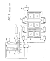
- Fig. 1 shows a block diagram of a prior art apparatus for vector comparing inspection.
- a photomask 1 is mounted on a stage 100 and light 3 is irradiated from beneath the photomask 1 so that two respective parts in two respective unit patterns can be caught by a.left optical system 201 and a right optical system 202.
- the left and right optical systems 201 and 202 respectively consist of lens systems 211 and 212 and image sensors 41 and 42.
- Each of the image sensors 41 and 42 consists of linear arrayed sensor elements and each element corresponds to the picture element of the unit pattern which satisfies the resolution required for the inspection.
- Each grouped video signal from the image sensor 41 and 42 is produced by scanning the stage 100 perpendicularly to the arrayed direction of the image sensor.
- the distance between the optical system 201 and 202 is adjusted so that the two optical images of respective parts in two respective unit patterns can be compared.
- the sequential comparison between two parts in respective unit patterns can be made by shifting the stage 100 stepwise and repeatedly.
- the above scanning and shifting of the stage 100 are controlled by a controller 11.
- the two grouped analog video signals from the image sensor 41 and 42 are sent to an amplitude distributor 5 in which the two grouped analog video signals are respectively converted to two grouped digital video signals so that the amplitude of each analog video signal is distributed into three levels such as white (W), tray (G), and black (B) corresponding to the amplitude being low, medium, and high. In these three levels, the level G is provided to prevent the occurrence of a false error.
- the two group digital video signals are stored as pattern data into a first left memory 12L and a first right memory 12R of an image memory 12 by means of left and right write-in unit 71 and 72, respectively, under the control of the controller 11.
- a minimum area as small as 0.5 ( ⁇ m) x 0.5 ( ⁇ m) is required for the inspecting resolution on the photomask pattern.
- the linear arrayed image sensor is constituted by as much as 512 sensing elements and if the scanning of the stage 100 is performed on a distance as long as the distance corresponding to 512 sensing elements, the resulting optical image is formed by 512 x 512 elements at the image plane of the optical system. This is equivalent to a size of 256 (pm) x 256 (pm) on the photomask 1, and this is the area of a comparing part in the unit pattern.
- each memory matrix in the first left and the first right memory 12L and 12R has 512 x 512 matrix elements.
- a quantity of pattern data as large as 512 x 512 matrix elements is too much to be inspected simultaneously with a high accuracy, so that the pattern data in the 512 x 512 matrix elements of each first memory 12L and 12R are separated into a set of 4 x 4 matrix elements and stored respectively into a second left memory 13L and a second right memory 13R of an image memory 13; these separation and memori- sation are respectively performed by means of a left separator 81 and a right one 82.
- the separated data become the subject of the vector comparing inspection and these separation and memorization are sequentially advanced each time the inspection of the separated data is over.
- any of the signal W, G, or B corresponds to a pattern datum in each matrix element of each second memory 13L or 13R, so, vector means can be used to form a boundary between neighboring elements.
- vectors are provided in four directions: left, right, up, and down, with equal magnitude, and the direction is determined by the following definition : when the datum B and W are adjacently arranged along longitude or latitude, the vector direction is defined from B to W; when the datum G is surrounded by the data W in all four directions, four vectors from G to W are provided along longitude and latitude; when the datum G is surrounded by the data B in all four directions, four vectors from B to G are provided along longitude and latitude; and when the data are arranged like B-G-W in longitude or latitude direction, G is changed to B so that only one vector from the changed B to W is provided.
- the vectors can be provided along longitude and latitude, but not along a diagonal.
- These vectors are generated by a left vector generator 91 and a right one 92, and the vector data are respectively fed to a left vector memory 14L and a right one 14R in a vector memory 14.
- the vector data in the vector memory 14L and 14R are compared by a vector comparator 10 in each one of the vector directions. For example, if there is a right directional vector in the left memory and no right directional vector in the right memory, the comparator 10 outputs the information that there is a defect; if there are two right directional vectors in the left memory and a right directional vector in the right memory, the comparator 10 outputs the information that there is no defect.
- the comparator 10 does not care of the total number of respective directional vectors in each memory, but only compares whether there are vectors having the same direction in the left and the right memory or not; this will be of significant importance for the present invention.
- Fig. 2 is a flow chart corresponding to the prior art inspecting apparatus shown in Fig. 1.
- Reference numerals in Fig. 2 are the same as the block numerals in Fig. 1, showing that the functions of the blocks exist there, except a stage coordinate memory 300 and an inspection output device 400.
- the vector comparator 10 produces a "NO" signal, this means that there is no defect; the signal is fed back to the separators 81 and 82 to control the inspection of the next separated patterns; when the vector comparator 10 outputs a "YES" signal, this means that there is a defect
- the stage coordinate memory 300 memorizes the stage position at the time when the defect is detected.
- the stage coordinate memory 300 controls the separators 81 and 82 to inspect the next separated patterns.
- the operator can check the detail of the inspection results by observing the data stored Ln the stage coordinate memory 300 on the inspection output device 400 such as cathode-ray tube or a sheet of printed paper.
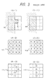
- FIG. 3 illustrates how the prior art vector comparing inspection is performed, showing an example of a defect on the photomask pattern.
- (a-1) and (b - 1) represent the optical images of the parts of the photomask pattern to be compared to each other.
- (a - 1) represents the optical image corresponding to the separated data in the second left memory 13L and (b - 1) represents that in the second right memory 13R.
- the pblique dotted lines located outside the square frame Ln (a - 1) and (b - 1) show how the optical image continues in the photomask pattern; a pattern 15L in (a - 1) has a defective part 20 and a pattern 15R in (b - 1) is assumed to be normal.
- a data matrix 16L in (a - 2) shows the separated data in the second left memory 13L
- a data matrix 16R in (b - 2) shows the separated data in the second right memory 13R
- Patterns 17L and 17R in (a - 3) and (b - 3) respectively show the vector patterns in the left vector memory 14 L and the right one 14R.
- the comparator 10 in Fig. 1 outputs the information that there is a defect in the photomask.
- the defective part 20 in the separated pattern 151 can be detected by the vector comparing inspection.
- the digital pattern datum at the defective part 20 was B in the above example.
- the patern datum is G
- the defect is as small as the half of the part 2 0
- the same results can be obtained, because the data including the defective part 20 are B - G-W in latitude and this arrangement is changed to B-B-W in the vector generator 91.
- the vector comparing inspection is effective to detect a very small defect, and further, importantly, the inspection can be made very quickly because it is performed only by comparing the directions of respective vector data.
- this inspection method it has been found that with this inspection method, some pattern is impossible to be detected even though the detected signal has enough amplitude like a datum B.
- Fig. 4 and 5 illustrate the problems which may arise with the vector comparing inspection of the prior art, by showing examples of indetectable defects.
- Fig. 4 shows a defect stuck out from a slant pattern.
- Fig. 5 shows square holes in respective separated patterns; corresponding sides of the square holes are parallel each other and the shapes are equal, but the sizes are different.
- FIG. 4 the situation of each illustration is the same as in Fig. 3.
- a separated pattern 15L in (a - 1) has a defective part 20 and a separated pattern 15R in (b - 1)is normal.
- the pattern data at the slant edge of the pattern are G. So, the data matrices in the separated memories 13L and 13R become as shown by data matrices 16L and 16R in (a - 2) and (b - 2), and the vector patterns in the vector memories 14L and 14R become as shown in (a - 3) and (b - 3). Comparing the vector patterns 17L and 17R, they appear to have the same quantity of vectors in every direction. This results as if there was no defect on the photomask pattern.
- the defect as mentioned in Fig. 4 or 5 often appears in the inspection of the photomask pattern.
- the problem of the square holes occurs in the inspection of a contact hole in a large scale integrated circuit; it is very important to solve
- an object of the present invention is to improve the prior art vector comparing method for photomask pattern inspection so that the defects which have been impossible to be detected by the prior art method can be detected by the vector comparing method and apparatus of the present invention.
- the method according to the present invention includes the steps which consist in : shifting paired separated data, which are separated from paired pattern data of respective optical images taken from the photomask pattern by optical systems and stored in respective separated data memories ,by a proper equal amount of memory elements to provide paired shifted data; synthesizing respectively the paired separated data and shifted data with a logical calculation of a B or a W priority logic providing paired synthesized data; storing the paired synthesized data in respective synthesized data memories; generating respectively vectors from the data arrangements in the paired synthesized memories in a latitudinal, a longitudinal, and a diagonal direction using relations among a datum B, G, and W; summing respectively the quantity of vectors each having a same direction in the paired vector memories; comparing between respective vector summations for detecting eventual differences between the summations; and producing an information indicative of a defect in the photomask pattern if a difference is detected in any comparison.
- any kind of defect in a photomask pattern can be detected with high accuracy, high sensitivity, and high speed.
- Fig. 6 shows a block diagram of an embodiment for a photomask inspecting apparatus applying a vector comparing method of the present invention.
- the elements of Figs. 1 and 6 having the same reference characters have the same functions and following units are added in the apparatus of Fig. 1:
- a left and a right data synthesizer 31 and 32 and a logic selector 30 the data synthesizers 31 and 32 respectively synthesize the shifted data and the original separated data providing paired synthesized data.
- the following data calculation must be considered: B + B, B + G, B + W, G + G, G + W, and W + W.
- a synthesized data memory 23 consisting of a left synthesized data memory 23L and a right one 23R: this memory stores the above synthesized data.
- a left vector generator 51 and a right one 52 their functions are almost equal to the vector generator 91 and 92 in Fig. 1 but the following two functions are added.
- a new treatment of the datum G is provided; that is, a vector is provided though the neighboring data includes the datum G like B - G or G - W; the vector from B to G is provided for the arrangement B - G and the vector from G to W is provided for the arrangement G - W.
- vectors along diagonals are provided; therefore, eight vectors can be used in total.
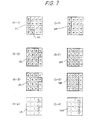
- Fig. 7 shows an example of inspection of the photomask pattern by the apparatus of the present invention, using the same separated patterns which has been used in Fig. 3.
- Fig. 7 (a - 1) and (b - 1) show the separated data stored respectively in the second memories 13L and 13R; thick solid lines show the respective separated patterns in which pattern 31L has a defective part 20 and pattern 31R is normal.
- These separated pattern data are respectively shifted by the data shifters 21 and 22; in this case, the shift amount is selected to be equal to two matrix elements and the shifting is performed toward a right and an up direction in the matrix of each second memory as shown by reference character 32L and 32R in (a - 2) and (b - 2) respectively; these figures are given only for explanation, they do not actually exist in memories.
- the original pattern data 31L and the shifted pattern data 32L, and the data 31R and 32R are respectively synthesized, to respective new patterns.
- the logical calculation "B priority logic" is applied in this case, so that the synthesized data become as shown by 33L and 33R in (a - 3) and (b - 3).
- the synthesized data are stored in the synthesized data memory 23, respectively in the left synthesized data memory 23L and the right one 23R.
- the left vector generator 51 and the right one 52 generate the vectors from the respective synthesized data, the generated vectors being such as shown by 34L and 34R in respective (a - 4) and (b - 4); these vectors are respectively stored in the left vector memory 14L and the right one 14R in the vector memory 14.
- the vector comparator 10 compares the summation of respective vectors in the vector memories 14L and 14R.
- the differences in the respective vectors of the eight kinds are as follows : up - 1, down - l, right - 1; diagonal (from left-up to right-down) -1; diagonal (from left-down to right-up) - 1; and the remaining differences are all zero.
- the vector comparator outputs the information that the photomask has a defect.
- there are differences of five kinds however, any one of these is sufficient to make the vector comparator 10 produce the defective information.
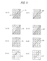
- the defect in the separated data mentioned above can also be detected by the prior art apparatus. However, the defects which will be shown in Figs. 8 and 9 and which are the same as those of Figs. 4 and 5 respectively, cannot be detected by the prior art technology.
- FIG. 8 show the separated data stored in the second memories 13L and 13R respectively; a pattern 31L has a defective part 20 and a pattern 31R is normal.
- (a - 2) and (b - 2) show the shifted pattern data; the shift amount is of one matrix element toward right and one matrix element in the up direction.
- (a - 3) and (b - 3) show the respective synthesized data; the synthesis is also made by applying the "B priority logic". From the synthesized data, respective vector signals can be obtained as shown in (a - 4) and (b - 4).
- the vector comparator 10 compares the summation of respective vectors in the vector memories 14L and 14R.
- the differences in the respective vectors of the eight kinds are as follows : up - 2, left - 2, diagonal (from right-down to left-up) - 2, diagonal (from left-down to right-up) - 1, diagonal (from right - up to left-down) - 1, and the remaining differences are all zero. Therefore, the vector comparator 10 outputs the information that the photomask has a defect.
- FIG. 9 (a - 1) and (b - 1) show the separated data stored in the second memory 13; in the separated patterns the square holes in pattern 31L and 31R should be equal in shape and size, but, actually, they are not equal in size.
- (a - 2) and (b - 2) show the respective shifted data; the shift amount is two matrix elements toward right.
- (a - 3) and (b-3) show the synthesized data; each synthesis is made by applying the "W priority logic”. From the synthesis data, respective vectors can be obtained as shown by (a - 4) and (b - 4).
- the vector comparator 10 compares the summation of respective vectors in the vector memories 14L and 14R.
- the differences in the respective vectors of the eight kinds are as follows : down - 4, diagonal (from left-up to right-down) - 3, diagonal (from right - up to left-down) - 3, and the remaining differences are all zero. Therefore, the vector comparator 10 outputs the information that the photomask has a defect.
- the determination of the shift amount and the selection of the B/W priority logic can be performed by the operator skilled in the art of the photomask inspection.
- the photomask inspection is required to be performed without the action of an operator, this can be met by providing the necessary software or hardware to perform sequentially several inspections in order to select properly the shift amount and the B/W priority logic. If a short inspecting time is required, this can be met by providing several data shifters in parallel, each for a particular shift amount, and the corresponding data synthesizers. So, several inspection outputs are obtained simultaneously, and if one of them produces an information indicative of a defect, it can be decided that the photomask has a defect.
- the threshold levels to provide the digital data B , G, and W in the amplitude distributor 5 and the shift amount set in the data shifters 21 and 22 can be selected properly considering the shape of the pattern or the size of the defect to be inspected.
- the detection sensitivity can be changed, considering the feature of the pattemto be inspected , by adjusting a threshold amount to be exceeded by the vector difference to produce the output information indicative of a defect. This is to avoid the occurrence of false errors.
- Fig. 10 is a flow chart relative to the inspecting apparatus of the present invention shown in Fig. 6; Fig. 10 has the same reference numerals as Fig.6, and reference numerals 300 and 400 are the same as in Fig. 2.
- the data shifters 21 and 22 in Fig. 10 shift the data read in the second memory 13.
- Fig. 11 shows a flow chart applying the image sharing immediately prior the image sensing. Compared to Fig. 10, the data shifters 21, 22 are cancelled and reference numeral 500 is added to show a block corresponding to an image sharing device. In this case, the image sharing is performed in relation to the second data memory 13 and the data synthesizers 31 and 32.
Landscapes
- Physics & Mathematics (AREA)
- General Physics & Mathematics (AREA)
- Engineering & Computer Science (AREA)
- Chemical & Material Sciences (AREA)
- Biochemistry (AREA)
- Pathology (AREA)
- Health & Medical Sciences (AREA)
- Life Sciences & Earth Sciences (AREA)
- Immunology (AREA)
- Analytical Chemistry (AREA)
- General Health & Medical Sciences (AREA)
- Computer Vision & Pattern Recognition (AREA)
- Quality & Reliability (AREA)
- Theoretical Computer Science (AREA)
- Investigating Materials By The Use Of Optical Means Adapted For Particular Applications (AREA)
- Preparing Plates And Mask In Photomechanical Process (AREA)
- Length Measuring Devices By Optical Means (AREA)
- Testing Or Measuring Of Semiconductors Or The Like (AREA)
Applications Claiming Priority (2)
| Application Number | Priority Date | Filing Date | Title |
|---|---|---|---|
| JP58171811A JPS6063405A (ja) | 1983-09-16 | 1983-09-16 | パタ−ン検査方法及びその装置 |
| JP171811/83 | 1983-09-16 |
Publications (3)
| Publication Number | Publication Date |
|---|---|
| EP0138665A2 true EP0138665A2 (fr) | 1985-04-24 |
| EP0138665A3 EP0138665A3 (en) | 1986-02-12 |
| EP0138665B1 EP0138665B1 (fr) | 1989-06-07 |
Family
ID=15930161
Family Applications (1)
| Application Number | Title | Priority Date | Filing Date |
|---|---|---|---|
| EP84401826A Expired EP0138665B1 (fr) | 1983-09-16 | 1984-09-14 | Méthode et appareil pour l'inspection de configurations de photomasques |
Country Status (5)
| Country | Link |
|---|---|
| US (1) | US4669123A (fr) |
| EP (1) | EP0138665B1 (fr) |
| JP (1) | JPS6063405A (fr) |
| KR (1) | KR910001247B1 (fr) |
| DE (1) | DE3478651D1 (fr) |
Cited By (4)
| Publication number | Priority date | Publication date | Assignee | Title |
|---|---|---|---|---|
| FR2637143A1 (fr) * | 1988-09-27 | 1990-03-30 | Allen Bradley Co | Dispositif de memorisation d'image video |
| EP0243639A3 (fr) * | 1986-04-17 | 1991-01-02 | International Business Machines Corporation | Système d'inspection automatique de motifs périodiques |
| FR2705479A1 (fr) * | 1993-05-17 | 1994-11-25 | Mitsubishi Electric Corp | Procédé et appareil de reconnaissance de formes. |
| USRE47980E1 (en) | 2002-07-22 | 2020-05-12 | Bromerc Limited | Process for removing mercury from flue gases |
Families Citing this family (18)
| Publication number | Priority date | Publication date | Assignee | Title |
|---|---|---|---|---|
| EP0186874B1 (fr) * | 1984-12-26 | 1994-06-08 | Hitachi, Ltd. | Procédé et appareil pour vérifier la géométrie des motifs multicouches pour des structures de circuits intégrés |
| DE3542484A1 (de) * | 1985-11-30 | 1987-07-02 | Ant Nachrichtentech | Verfahren zur erkennung von kantenstrukturen in einem bildsignal |
| EP0236738A3 (fr) * | 1986-02-05 | 1988-12-21 | OMRON Corporation | Procédé d'entrée de dates d'une plaque à circuits imprimés équipée de référence pour le traitement d'images d'un appareil d'inspection automatique de plaques à circuits imprimés équipées |
| US4805123B1 (en) * | 1986-07-14 | 1998-10-13 | Kla Instr Corp | Automatic photomask and reticle inspection method and apparatus including improved defect detector and alignment sub-systems |
| US5091963A (en) * | 1988-05-02 | 1992-02-25 | The Standard Oil Company | Method and apparatus for inspecting surfaces for contrast variations |
| DE3905234A1 (de) * | 1989-02-21 | 1990-08-30 | Weber Joerg | Verfahren zum erzeugen eines die unterschiede zwischen zwei einander zugeordneten bildern verdeutlichenden dritten bildes |
| US4918382A (en) * | 1989-03-20 | 1990-04-17 | Tektronix, Inc. | Method for distinguishing between real and spurious responses in a spectrum analyzer |
| US5199082A (en) * | 1989-09-11 | 1993-03-30 | U.S. Philips Corp. | Method of detecting an amplitude transient in a field of elements having a multivalent amplitude distribution, device suitable for performing the method, and video system including the device |
| US5392360A (en) * | 1993-04-28 | 1995-02-21 | International Business Machines Corporation | Method and apparatus for inspection of matched substrate heatsink and hat assemblies |
| JPH10177589A (ja) * | 1996-12-18 | 1998-06-30 | Mitsubishi Electric Corp | パターン比較検証装置、パターン比較検証方法およびパターン比較検証プログラムを記録した媒体 |
| US6091845A (en) * | 1998-02-24 | 2000-07-18 | Micron Technology, Inc. | Inspection technique of photomask |
| US6947587B1 (en) * | 1998-04-21 | 2005-09-20 | Hitachi, Ltd. | Defect inspection method and apparatus |
| US6888958B1 (en) * | 1999-03-30 | 2005-05-03 | Kabushiki Kaisha Toshiba | Method and apparatus for inspecting patterns |
| JP4265722B2 (ja) * | 2000-08-07 | 2009-05-20 | 富士通マイクロエレクトロニクス株式会社 | パターンデータ修正方法及び装置 |
| US7558419B1 (en) * | 2003-08-14 | 2009-07-07 | Brion Technologies, Inc. | System and method for detecting integrated circuit pattern defects |
| AT502810B1 (de) * | 2005-11-17 | 2007-06-15 | Arc Seibersdorf Res Gmbh | Verfahren zur optischen prüfung von gegenständen |
| JP2007142275A (ja) * | 2005-11-21 | 2007-06-07 | Toshiba Corp | フォトマスクの判定方法、半導体装置の製造方法及びプログラム |
| EP3982326B1 (fr) * | 2020-07-27 | 2024-07-31 | Changxin Memory Technologies, Inc. | Procédé d'acquisition de modèle de défaillance et appareil d'acquisition |
Family Cites Families (5)
| Publication number | Priority date | Publication date | Assignee | Title |
|---|---|---|---|---|
| GB1401008A (en) * | 1971-08-17 | 1975-07-16 | Mullared Ltd | Character recognition apparatus |
| JPS5371563A (en) * | 1976-12-08 | 1978-06-26 | Hitachi Ltd | Automatic inspection correcting method for mask |
| US4345312A (en) * | 1979-04-13 | 1982-08-17 | Hitachi, Ltd. | Method and device for inspecting the defect of a pattern represented on an article |
| US4490848A (en) * | 1982-03-31 | 1984-12-25 | General Electric Company | Method and apparatus for sorting corner points in a visual image processing system |
| US4532650A (en) * | 1983-05-12 | 1985-07-30 | Kla Instruments Corporation | Photomask inspection apparatus and method using corner comparator defect detection algorithm |
-
1983
- 1983-09-16 JP JP58171811A patent/JPS6063405A/ja active Granted
-
1984
- 1984-09-14 DE DE8484401826T patent/DE3478651D1/de not_active Expired
- 1984-09-14 EP EP84401826A patent/EP0138665B1/fr not_active Expired
- 1984-09-15 KR KR1019840005630A patent/KR910001247B1/ko not_active Expired
- 1984-09-17 US US06/651,086 patent/US4669123A/en not_active Expired - Lifetime
Cited By (4)
| Publication number | Priority date | Publication date | Assignee | Title |
|---|---|---|---|---|
| EP0243639A3 (fr) * | 1986-04-17 | 1991-01-02 | International Business Machines Corporation | Système d'inspection automatique de motifs périodiques |
| FR2637143A1 (fr) * | 1988-09-27 | 1990-03-30 | Allen Bradley Co | Dispositif de memorisation d'image video |
| FR2705479A1 (fr) * | 1993-05-17 | 1994-11-25 | Mitsubishi Electric Corp | Procédé et appareil de reconnaissance de formes. |
| USRE47980E1 (en) | 2002-07-22 | 2020-05-12 | Bromerc Limited | Process for removing mercury from flue gases |
Also Published As
| Publication number | Publication date |
|---|---|
| DE3478651D1 (en) | 1989-07-13 |
| JPH0245124B2 (fr) | 1990-10-08 |
| JPS6063405A (ja) | 1985-04-11 |
| EP0138665A3 (en) | 1986-02-12 |
| EP0138665B1 (fr) | 1989-06-07 |
| KR910001247B1 (ko) | 1991-02-26 |
| US4669123A (en) | 1987-05-26 |
| KR850002697A (ko) | 1985-05-15 |
Similar Documents
| Publication | Publication Date | Title |
|---|---|---|
| EP0138665B1 (fr) | Méthode et appareil pour l'inspection de configurations de photomasques | |
| US7260256B2 (en) | Method and system for inspecting a pattern | |
| US4776023A (en) | Pattern inspection method | |
| US4969198A (en) | System for automatic inspection of periodic patterns | |
| EP0243639B1 (fr) | Système d'inspection automatique de motifs périodiques | |
| US4532650A (en) | Photomask inspection apparatus and method using corner comparator defect detection algorithm | |
| US6865288B1 (en) | Pattern inspection method and apparatus | |
| US5119434A (en) | Method of and apparatus for geometric pattern inspection employing intelligent imaged-pattern shrinking, expanding and processing to identify predetermined features and tolerances | |
| US20120207382A1 (en) | Fault inspection method | |
| JPH01224881A (ja) | パターン検査装置 | |
| JP2005529388A (ja) | パターン検査方法 | |
| JPH0571991B2 (fr) | ||
| GB2286670A (en) | Detecting surface defects | |
| US4778745A (en) | Defect detection method of semiconductor wafer patterns | |
| US5440650A (en) | Image processing system for inspection of overprinted matter | |
| EP0673150A2 (fr) | Procédé et appareil pour la génération d'images en demi-teintes | |
| JPS6083328A (ja) | フオトマスクの検査方法 | |
| KR19990063507A (ko) | 이미지 결함 검출 장치 및 방법 | |
| KR900001268B1 (ko) | 패턴 검사방법 및 장치 | |
| EP1619552A2 (fr) | Méthode de conception d'un masque d'exposition par faisceau de particules chargées, masque d'exposition par faisceau de particules chargées et méthode d'exposition utilisant ce masque | |
| US4475037A (en) | Method of inspecting a mask using an electron beam vector scan system | |
| KR970007974B1 (ko) | 반도체 공정결함 검사방법 | |
| Cruttwell | A Fully Automated Pattern Inspection System for Reticles & Masks | |
| JP2000294139A (ja) | 周期性パターンの欠陥検査方法及び装置 | |
| JPH0774787B2 (ja) | 多層パタ−ン欠陥検出方法及びその装置 |
Legal Events
| Date | Code | Title | Description |
|---|---|---|---|
| PUAI | Public reference made under article 153(3) epc to a published international application that has entered the european phase |
Free format text: ORIGINAL CODE: 0009012 |
|
| AK | Designated contracting states |
Designated state(s): DE FR GB |
|
| PUAL | Search report despatched |
Free format text: ORIGINAL CODE: 0009013 |
|
| RHK1 | Main classification (correction) |
Ipc: G06K 9/62 |
|
| AK | Designated contracting states |
Designated state(s): DE FR GB |
|
| 17P | Request for examination filed |
Effective date: 19860723 |
|
| 17Q | First examination report despatched |
Effective date: 19871006 |
|
| GRAA | (expected) grant |
Free format text: ORIGINAL CODE: 0009210 |
|
| AK | Designated contracting states |
Kind code of ref document: B1 Designated state(s): DE FR GB |
|
| REF | Corresponds to: |
Ref document number: 3478651 Country of ref document: DE Date of ref document: 19890713 |
|
| ET | Fr: translation filed | ||
| PLBE | No opposition filed within time limit |
Free format text: ORIGINAL CODE: 0009261 |
|
| STAA | Information on the status of an ep patent application or granted ep patent |
Free format text: STATUS: NO OPPOSITION FILED WITHIN TIME LIMIT |
|
| 26N | No opposition filed | ||
| PGFP | Annual fee paid to national office [announced via postgrant information from national office to epo] |
Ref country code: DE Payment date: 19931121 Year of fee payment: 10 |
|
| PG25 | Lapsed in a contracting state [announced via postgrant information from national office to epo] |
Ref country code: DE Effective date: 19950601 |
|
| REG | Reference to a national code |
Ref country code: GB Ref legal event code: IF02 |
|
| PGFP | Annual fee paid to national office [announced via postgrant information from national office to epo] |
Ref country code: FR Payment date: 20030909 Year of fee payment: 20 |
|
| PGFP | Annual fee paid to national office [announced via postgrant information from national office to epo] |
Ref country code: GB Payment date: 20030910 Year of fee payment: 20 |
|
| PG25 | Lapsed in a contracting state [announced via postgrant information from national office to epo] |
Ref country code: GB Free format text: LAPSE BECAUSE OF EXPIRATION OF PROTECTION Effective date: 20040913 |
|
| REG | Reference to a national code |
Ref country code: GB Ref legal event code: PE20 |