EP0138675A2 - Virtuelle Adressabbildung mit einem zweistufigen Umsetzungspuffer - Google Patents
Virtuelle Adressabbildung mit einem zweistufigen Umsetzungspuffer Download PDFInfo
- Publication number
- EP0138675A2 EP0138675A2 EP84401882A EP84401882A EP0138675A2 EP 0138675 A2 EP0138675 A2 EP 0138675A2 EP 84401882 A EP84401882 A EP 84401882A EP 84401882 A EP84401882 A EP 84401882A EP 0138675 A2 EP0138675 A2 EP 0138675A2
- Authority
- EP
- European Patent Office
- Prior art keywords
- translation
- virtual address
- translation buffer
- address
- entry
- Prior art date
- Legal status (The legal status is an assumption and is not a legal conclusion. Google has not performed a legal analysis and makes no representation as to the accuracy of the status listed.)
- Withdrawn
Links
Images
Classifications
-
- G—PHYSICS
- G06—COMPUTING OR CALCULATING; COUNTING
- G06F—ELECTRIC DIGITAL DATA PROCESSING
- G06F12/00—Accessing, addressing or allocating within memory systems or architectures
- G06F12/02—Addressing or allocation; Relocation
- G06F12/08—Addressing or allocation; Relocation in hierarchically structured memory systems, e.g. virtual memory systems
- G06F12/10—Address translation
- G06F12/1027—Address translation using associative or pseudo-associative address translation means, e.g. translation look-aside buffer [TLB]
-
- G—PHYSICS
- G06—COMPUTING OR CALCULATING; COUNTING
- G06F—ELECTRIC DIGITAL DATA PROCESSING
- G06F2212/00—Indexing scheme relating to accessing, addressing or allocation within memory systems or architectures
- G06F2212/68—Details of translation look-aside buffer [TLB]
- G06F2212/681—Multi-level TLB, e.g. microTLB and main TLB
Definitions
- the present invention relates to memory management systems using virtual-to-physical address mapping, and more specifically to virtual mappings using, in addition to a conventional main-memory translation level, a two-level translation buffer.
- a virtual address to be translated is divided in two parts.
- a first part is used without translation as the least significant part of the physical address.
- a second part is then used to access a look-up table stored in memory holding the physical addresses.
- the second part is typically divided in three subparts, a first subpart being used to select one of a number of look-up tables addressed by the second subpart, and a corresponding second look-up table being addressed by the third subpart. Since the look-up tables mapping a large virtual memory space into a smaller physical memory space are large, they must be held in memory.
- the translation uses two additional memory references; thus, to obtain an actual address it takes as many as three memory references.
- a second level of translation is implemented by using a translation buffer, also called a dynamic look-aside table.
- a translation buffer holds a number of two-part entries, with each entry having as the first part a virtual address and asf the second part the corresponding physical address. Since the:translation buffer is formed by hardware registers, the physical address is immediately available without a memory reference if a virtual address is found in the translation buffer. Of course, if the virtual address is not found in the translation buffer, then the system reverts back to the first level of translation and its corresponding three memory references. Once a virtual address has been translated this way, it and its corresponding physical address are entered in the translation buffer, for future reference.
- a large translation buffer can be provided, thus limiting the instances when the slow first translation level is needed.
- a large translation buffer cannot be used, since it requires a large area, leaving not enough room for anything else. In this case a small translation buffer may be used.
- the problem, then, is that by using a small translation buffer, i.e. very few entries, the number of-instances when the virtual address will not be found on the translation buffer will be great. This means that the slow first level translation is needed often, slowing down the system and impairing performance.
- the present invention provides for a small processor having a two-level translation buffer for improved performance. This is achieved by using a first translation buffer, for just a few entries, on the instruction execution subsystem, and a second translation buffer, containing a much larger number of entries, on a separate subsystem.
- the present invention further provides for a computer system, including a processor subsystem using virtual memory, in which address translation means comprise first translation buffer means for translating a selected virtual address into a physical address, the first means being located within the processor subsystem and having a predetermined first number of virtual/physical address entries second translation buffer means for translating the selected virtual address into a physical address upon a missed match in the first translation buffer means, the second means being located off the processor subsystem and having a predetermined second number, greater than the first, of virtual/physical address entries, and means for translating upon a missed match in the second translation buffer means the selected virtual address into a physical address from tables stored in memory.
- address translation means comprise first translation buffer means for translating a selected virtual address into a physical address, the first means being located within the processor subsystem and having a predetermined first number of virtual/physical address entries second translation buffer means for translating the selected virtual address into a physical address upon a missed match in the first translation buffer means, the second means being located off the processor subsystem and having a predetermined second number, greater than the first,
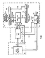
- Fig. 1 there is shown a functional block diagram of the memory mapping system of the present invention. It comprises Microprocessor subsystem 10, Backup Translation Buffer (BTB) subsystem 60, and Main Memory subsystem 70. Only those components of Microprocessor subsystem 10 related to address translation are shown in the figure, since all the other components of a microprocessor using virtual addressing are well known in the art. In the preferred embodiment Microprocessor subsystem 10 and BTB subsystem 60 are implemented as separate integrated circuits.
- Microprocessor subsystem 10 comprises a conventional Address Calculation circuit 20, which is used in the figure to encompass all the various circuits that are needed in a typical microprocessor to produce, for a particular instruction, the virtual address to be translated into a physical address.
- the virtual address thus calculated is then fed over lines 22 to Virtual Address Register 30.
- a first part 30A of Virtual Address Register 30, corresponding to a predetermined number of least significant address bits, is coupled directly through lines 32 to a corresponding first part 50A of Physical Address Register 50, to be used as the physical address bits defining the address within a given page frame of physical memory.
- a second part 30 B of Virtual Address Register 30 is sent over lines 34 to Mini-Translation Buffer (mini-TB) 40.
- mini-TB 40 Mini-Translation Buffer
- the physical address corresponding to the matched virtual address entry is loaded via lines 42 onto second part 50B of Physical Address Register 50, to be used as the physical address bits defining a page frame number.
- Physical Address Register 50 then loads the entire physical address on the Physical Address Bus 52. This level of translation is done during the tail end of the cycle in which the virtual address is loaded on Register 30. Since this translation involves only local register accesses, it is completed before the end of the cycle.
- a No Match signal 44 is generated and sent to Backup Translation Buffer 62 along with the second portion 30B of the virtual address which is sent over lines 46.
- BTB 62 is similar to mini-TB 40, the difference being only in the much greater number of entries, or the translation buffer of a VAX-11/780 or IBM 370 computer can be used.
- the virtual address portion 30B is now compared with one or more entries that are part of BTB 62. If a match is found, the physical address corresponding to the matched virtual ddress entry is sent back over lines 48 to mini-TB 40 to be overwritten, along with the virtual address being translated, on a predetermined Mini-TB 40 entry.
- Mini-TB 40 generates an Enable Mini-TB Load Signal 56 for this purpose.
- the fill or replacement algorithm will be discussed below.
- the mini-TB level translation is then retried and the physical address is loaded by the mini-TB on the corresponding portion of Physical Register 50. Since the BTB level of translation involves access of registers in a different subsystem, i.e. off-chip in an integrated circuit implementation, it is not completed within the same cycle, but requires only one extra cycle.
- BTB 62 If a match is not found on the BTB, BTB 62 generates and sends a No-BTB-Match Signal 64 'to BTB-Miss Sequencer 54.
- BTB-Miss Sequencer 54 uses this signal to perform a conventional translation using tables stored in Main Memory 72, and includes the required standard microprocessor circuitry and/or microcode, as is well known in the art. Once the translation is done, the physical address is placed, from memory 72, on lines 68 and 48 for access by BTB 62 and mini-TB 40.
- Sequencer 54 also generates Enable mini-TB Load Signal 56' and Enable BTB Load Signal 58 to load the physical address on lines 68 and 48 and the virtual address on lines 46 and 34 in corresponding registers of, respectively, BTB 62 and mini-TB 40._The mini-TB level translation is then retried and the physical address is loaded by the mini-TB on the corresponding portion of Physical Address Register 50.
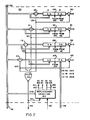
- FIG. 2 there is shown a more detailed block diagram for mini-TB 40. It comprises four Storage Registers 100 through 103. Each storage register has two parts. A first part A stores a virtual address, and a second part B stores a corresponding physical address.. The virtual address calculated in Address Calculator 20, sent over lines 34, is then compared with the virtual address entries 100A through 103A by means of comparators 110 through 113. Each comparator 110 through 113 asserts a corresponding signal, 120 through 123 respectively, if a match is found. j
- a corresponding one of comparator signals 120 through 123 also enables a corresponding Bus Driver 130 through 133 to load the physical address portion B corresponding to the matched virtual address onto the Physical Address bus 42. :
- Register Load Signals 151 through 154 control the loading of Registers 100 through 103.
- One of Register Load Signals 151 through 154 will be set by Replacement Selection Circuit 150, as a function of the two least significant bits of the Virtual address, if so enabled by Enable mini-TB Load signal 56 or 56'.
Landscapes
- Engineering & Computer Science (AREA)
- Theoretical Computer Science (AREA)
- Physics & Mathematics (AREA)
- General Engineering & Computer Science (AREA)
- General Physics & Mathematics (AREA)
- Memory System Of A Hierarchy Structure (AREA)
Applications Claiming Priority (2)
| Application Number | Priority Date | Filing Date | Title |
|---|---|---|---|
| US53596783A | 1983-09-22 | 1983-09-22 | |
| US535967 | 1990-06-08 |
Publications (2)
| Publication Number | Publication Date |
|---|---|
| EP0138675A2 true EP0138675A2 (de) | 1985-04-24 |
| EP0138675A3 EP0138675A3 (de) | 1986-12-30 |
Family
ID=24136557
Family Applications (1)
| Application Number | Title | Priority Date | Filing Date |
|---|---|---|---|
| EP84401882A Withdrawn EP0138675A3 (de) | 1983-09-22 | 1984-09-21 | Virtuelle Adressabbildung mit einem zweistufigen Umsetzungspuffer |
Country Status (2)
| Country | Link |
|---|---|
| EP (1) | EP0138675A3 (de) |
| JP (1) | JPS60150148A (de) |
Cited By (5)
| Publication number | Priority date | Publication date | Assignee | Title |
|---|---|---|---|---|
| EP0254270A3 (en) * | 1986-07-21 | 1990-04-04 | Honeywell Bull Inc. | High speed high density dynamic address translator |
| EP0704805A3 (de) * | 1994-09-28 | 1996-07-31 | Toshiba Kk | Adressenübersetzungsvorrichtung |
| EP0747826A3 (de) * | 1995-06-06 | 1998-04-01 | Hewlett-Packard Company | Cache-Speicheranordnung mit gleichzeitigem Etikettenvergleich |
| WO2007048134A1 (en) * | 2005-10-20 | 2007-04-26 | Qualcomm Incorporated | Updating multiple levels of translation lookaside buffers (tlbs) field |
| EP4152163A4 (de) * | 2020-06-11 | 2023-11-15 | Huawei Technologies Co., Ltd. | Verfahren zur verarbeitung von metadaten in einer speichervorrichtung und zugehörige vorrichtung |
Families Citing this family (1)
| Publication number | Priority date | Publication date | Assignee | Title |
|---|---|---|---|---|
| JPH04128946A (ja) * | 1990-09-20 | 1992-04-30 | Fujitsu Ltd | アドレス変換方式 |
Family Cites Families (1)
| Publication number | Priority date | Publication date | Assignee | Title |
|---|---|---|---|---|
| JPS5557965A (en) * | 1977-12-29 | 1980-04-30 | Toshiba Corp | Address converter |
-
1984
- 1984-09-21 JP JP59198421A patent/JPS60150148A/ja active Pending
- 1984-09-21 EP EP84401882A patent/EP0138675A3/de not_active Withdrawn
Cited By (8)
| Publication number | Priority date | Publication date | Assignee | Title |
|---|---|---|---|---|
| EP0254270A3 (en) * | 1986-07-21 | 1990-04-04 | Honeywell Bull Inc. | High speed high density dynamic address translator |
| EP0704805A3 (de) * | 1994-09-28 | 1996-07-31 | Toshiba Kk | Adressenübersetzungsvorrichtung |
| US5860145A (en) * | 1994-09-28 | 1999-01-12 | Kabushiki Kaisha Toshiba | Address translation device storage last address translation in register separate from TLB |
| EP0747826A3 (de) * | 1995-06-06 | 1998-04-01 | Hewlett-Packard Company | Cache-Speicheranordnung mit gleichzeitigem Etikettenvergleich |
| US5860078A (en) * | 1995-06-06 | 1999-01-12 | Hewlett-Packard Company | Multiple input two-level cache directory with mini-directory for initial comparisons and main directory for mini-directory misses |
| WO2007048134A1 (en) * | 2005-10-20 | 2007-04-26 | Qualcomm Incorporated | Updating multiple levels of translation lookaside buffers (tlbs) field |
| EP4152163A4 (de) * | 2020-06-11 | 2023-11-15 | Huawei Technologies Co., Ltd. | Verfahren zur verarbeitung von metadaten in einer speichervorrichtung und zugehörige vorrichtung |
| US12223171B2 (en) | 2020-06-11 | 2025-02-11 | Huawei Technologies Co., Ltd. | Metadata processing method to improve data read/write efficiency of a storage device |
Also Published As
| Publication number | Publication date |
|---|---|
| EP0138675A3 (de) | 1986-12-30 |
| JPS60150148A (ja) | 1985-08-07 |
Similar Documents
| Publication | Publication Date | Title |
|---|---|---|
| EP0232526B1 (de) | Seitenorganisierter Cachespeicher mit virtueller Adressierung | |
| US5412787A (en) | Two-level TLB having the second level TLB implemented in cache tag RAMs | |
| US6138208A (en) | Multiple level cache memory with overlapped L1 and L2 memory access | |
| US5475827A (en) | Dynamic look-aside table for multiple size pages | |
| US5787494A (en) | Software assisted hardware TLB miss handler | |
| US6772315B1 (en) | Translation lookaside buffer extended to provide physical and main-memory addresses | |
| US4769770A (en) | Address conversion for a multiprocessor system having scalar and vector processors | |
| US5182805A (en) | Method and system for determining copy-on-write condition | |
| JPH04319747A (ja) | アドレス変換機構 | |
| GB1487078A (en) | Buffered virtual storage and data processing system | |
| US5956752A (en) | Method and apparatus for accessing a cache using index prediction | |
| US4821171A (en) | System of selective purging of address translation in computer memories | |
| JPH0312339B2 (de) | ||
| JP2000227874A (ja) | コンピュ―タ・システムにおいてディレクトリ構造を含むメイン・メモリの内容にアドレスするための方法および装置 | |
| US5710905A (en) | Cache controller for a non-symetric cache system | |
| EP0138675A2 (de) | Virtuelle Adressabbildung mit einem zweistufigen Umsetzungspuffer | |
| US5954812A (en) | Apparatus for caching system management memory in a computer having a system management mode employing address translation | |
| US5732405A (en) | Method and apparatus for performing a cache operation in a data processing system | |
| EP0239359B1 (de) | Adressübersetzungsschaltung | |
| US6212616B1 (en) | Even/odd cache directory mechanism | |
| JPH07281947A (ja) | 入出力アドレス用変換装置 | |
| US20050177701A1 (en) | Address coversion technique in a context switching environment | |
| US6397297B1 (en) | Dual cache with multiple interconnection operation modes | |
| EP0395835A2 (de) | Cache-Speicherzugriffsverfahren und Anordnung | |
| JP2002312239A (ja) | プロセッサ、システムオンチップ装置及びアクセス方法 |
Legal Events
| Date | Code | Title | Description |
|---|---|---|---|
| PUAI | Public reference made under article 153(3) epc to a published international application that has entered the european phase |
Free format text: ORIGINAL CODE: 0009012 |
|
| AK | Designated contracting states |
Designated state(s): DE FR GB |
|
| PUAL | Search report despatched |
Free format text: ORIGINAL CODE: 0009013 |
|
| AK | Designated contracting states |
Kind code of ref document: A3 Designated state(s): DE FR GB |
|
| 17P | Request for examination filed |
Effective date: 19870306 |
|
| 17Q | First examination report despatched |
Effective date: 19880405 |
|
| STAA | Information on the status of an ep patent application or granted ep patent |
Free format text: STATUS: THE APPLICATION IS DEEMED TO BE WITHDRAWN |
|
| 18D | Application deemed to be withdrawn |
Effective date: 19900602 |
|
| RIN1 | Information on inventor provided before grant (corrected) |
Inventor name: NGUYEN, LE TRONG Inventor name: LACKEY, STANLEY A. Inventor name: HERRICK, WILLIAM V. Inventor name: SITES, RICHARD L. |