EP0139583A2 - Quarzoszillator für sehr hohe Frequenzen - Google Patents
Quarzoszillator für sehr hohe Frequenzen Download PDFInfo
- Publication number
- EP0139583A2 EP0139583A2 EP84402015A EP84402015A EP0139583A2 EP 0139583 A2 EP0139583 A2 EP 0139583A2 EP 84402015 A EP84402015 A EP 84402015A EP 84402015 A EP84402015 A EP 84402015A EP 0139583 A2 EP0139583 A2 EP 0139583A2
- Authority
- EP
- European Patent Office
- Prior art keywords
- oscillator
- frequency
- quartz
- oscillator according
- loop
- Prior art date
- Legal status (The legal status is an assumption and is not a legal conclusion. Google has not performed a legal analysis and makes no representation as to the accuracy of the status listed.)
- Granted
Links
- 239000010453 quartz Substances 0.000 claims abstract description 39
- VYPSYNLAJGMNEJ-UHFFFAOYSA-N silicon dioxide Inorganic materials O=[Si]=O VYPSYNLAJGMNEJ-UHFFFAOYSA-N 0.000 claims abstract description 39
- 239000003990 capacitor Substances 0.000 claims description 36
- 230000006978 adaptation Effects 0.000 claims description 26
- 230000010363 phase shift Effects 0.000 claims description 8
- 230000001186 cumulative effect Effects 0.000 claims description 2
- 239000013078 crystal Substances 0.000 abstract 1
- 238000010586 diagram Methods 0.000 description 6
- 238000003780 insertion Methods 0.000 description 6
- 230000037431 insertion Effects 0.000 description 6
- 230000035939 shock Effects 0.000 description 3
- 230000015556 catabolic process Effects 0.000 description 2
- 238000006731 degradation reaction Methods 0.000 description 2
- 239000012528 membrane Substances 0.000 description 2
- 238000000034 method Methods 0.000 description 2
- 230000010287 polarization Effects 0.000 description 2
- 238000011144 upstream manufacturing Methods 0.000 description 2
- 241000282552 Chlorocebus aethiops Species 0.000 description 1
- 230000001627 detrimental effect Effects 0.000 description 1
- 230000000694 effects Effects 0.000 description 1
- 238000001914 filtration Methods 0.000 description 1
- 238000005259 measurement Methods 0.000 description 1
- 238000005070 sampling Methods 0.000 description 1
- 238000001228 spectrum Methods 0.000 description 1
Images



Classifications
-
- H—ELECTRICITY
- H03—ELECTRONIC CIRCUITRY
- H03B—GENERATION OF OSCILLATIONS, DIRECTLY OR BY FREQUENCY-CHANGING, BY CIRCUITS EMPLOYING ACTIVE ELEMENTS WHICH OPERATE IN A NON-SWITCHING MANNER; GENERATION OF NOISE BY SUCH CIRCUITS
- H03B5/00—Generation of oscillations using amplifier with regenerative feedback from output to input
- H03B5/30—Generation of oscillations using amplifier with regenerative feedback from output to input with frequency-determining element being electromechanical resonator
- H03B5/32—Generation of oscillations using amplifier with regenerative feedback from output to input with frequency-determining element being electromechanical resonator being a piezoelectric resonator
- H03B5/36—Generation of oscillations using amplifier with regenerative feedback from output to input with frequency-determining element being electromechanical resonator being a piezoelectric resonator active element in amplifier being semiconductor device
-
- H—ELECTRICITY
- H03—ELECTRONIC CIRCUITRY
- H03B—GENERATION OF OSCILLATIONS, DIRECTLY OR BY FREQUENCY-CHANGING, BY CIRCUITS EMPLOYING ACTIVE ELEMENTS WHICH OPERATE IN A NON-SWITCHING MANNER; GENERATION OF NOISE BY SUCH CIRCUITS
- H03B5/00—Generation of oscillations using amplifier with regenerative feedback from output to input
- H03B5/18—Generation of oscillations using amplifier with regenerative feedback from output to input with frequency-determining element comprising distributed inductance and capacitance
- H03B5/1841—Generation of oscillations using amplifier with regenerative feedback from output to input with frequency-determining element comprising distributed inductance and capacitance the frequency-determining element being a strip line resonator
- H03B5/1847—Generation of oscillations using amplifier with regenerative feedback from output to input with frequency-determining element comprising distributed inductance and capacitance the frequency-determining element being a strip line resonator the active element in the amplifier being a semiconductor device
-
- H—ELECTRICITY
- H03—ELECTRONIC CIRCUITRY
- H03B—GENERATION OF OSCILLATIONS, DIRECTLY OR BY FREQUENCY-CHANGING, BY CIRCUITS EMPLOYING ACTIVE ELEMENTS WHICH OPERATE IN A NON-SWITCHING MANNER; GENERATION OF NOISE BY SUCH CIRCUITS
- H03B5/00—Generation of oscillations using amplifier with regenerative feedback from output to input
- H03B5/30—Generation of oscillations using amplifier with regenerative feedback from output to input with frequency-determining element being electromechanical resonator
- H03B5/32—Generation of oscillations using amplifier with regenerative feedback from output to input with frequency-determining element being electromechanical resonator being a piezoelectric resonator
- H03B5/36—Generation of oscillations using amplifier with regenerative feedback from output to input with frequency-determining element being electromechanical resonator being a piezoelectric resonator active element in amplifier being semiconductor device
- H03B5/366—Generation of oscillations using amplifier with regenerative feedback from output to input with frequency-determining element being electromechanical resonator being a piezoelectric resonator active element in amplifier being semiconductor device and comprising means for varying the frequency by a variable voltage or current
- H03B5/368—Generation of oscillations using amplifier with regenerative feedback from output to input with frequency-determining element being electromechanical resonator being a piezoelectric resonator active element in amplifier being semiconductor device and comprising means for varying the frequency by a variable voltage or current the means being voltage variable capacitance diodes
Definitions
- the present invention relates to a quartz oscillator for very high frequencies.
- the invention proposes an electronic diagram of a quartz oscillator which makes it possible to reach frequencies at least equal to 1 GHz in direct frequency.
- the oscillator according to the invention comprises an amplifier and a feedback loop comprising a quartz, a given resonant frequency of which is chosen as the frequency of the oscillator, the amplifier having a gain such as in open loop, the condition Berkhausen's gain is satisfied.
- the quartz is compensated at said frequency by a parallel circuit comprising at least one choke
- the feedback loop also includes a filter ensuring a cut-off of the frequencies below said resonant frequency, in that that the feedback loop is such that at said resonant frequency, on the one hand, it is adapted in impedance so that the compensation of the quartz is itself adapted and on the other on the other hand, it has a zero phase shift to within 2k ⁇ , and in that it comprises a power divider making it possible to take a part of the signal from the feedback loop to inject it into an output amplifier.
- the amplifier is preferably a transistor mounted as a common emitter.
- the parallel circuit includes a compensation capacitor, in particular a variable capacitor.
- the feedback loop includes an electronic frequency tuning circuit.
- This tuning circuit may include a fixed capacitor arranged in series in the feedback loop and at the terminals of which is connected a Varicap diode supplied by a voltage control circuit.
- Said filter ensuring a cut-off of frequencies below the resonant frequency advantageously comprises a ⁇ filter comprising a variable series capacitor surrounded by two reactors, one terminal of which is grounded.
- the oscillator is produced in the form of a line. It comprises discrete components distributed along the line sections of the loop so as to achieve the impedance adaptation of the loop and the cumulative length of the line sections is such that the loop has a zero phase shift to within 2k ⁇ .
- the filter mentioned above is a T r filter
- the two inductors can be sections of lines of length less than a quarter of the wavelength of the frequency of the oscillator.
- the power divider can be a Wilkinson type power divider.
- an oscillator essentially consists of an amplifier A, having a gain A Q (w), feedback from a quadrupole having a response curve B ( w ).
- the product A 0 ⁇ must be very slightly greater than 1 at the frequency of the oscillator. More precisely, the open loop gain A 0 ⁇ expressed in decibels must be equal to approximately 2 to 3 decibels. This represents the Berkhausen winning condition.
- any oscillator hangs on a frequency for which the total phase shift in open loop is zero modulo 2 ⁇ .
- such a UHF quartz is in the form of a disc 1 in which a bowl 2 has been dug delimiting a thin membrane 5, the thickness of which is a few microns therefore presenting a partial 5 of frequency f 0 close to 1 GHz.
- Each face of the membrane 5 carries an electrode, one 3 being located in the bowl 2, and the other 4 being located on the underside of the disc 1.
- a compensation inductor L n is connected to the terminals of the quartz so as to produce a plug circuit at the frequency f 0 eliminating the harmful influence of C 0 .
- ⁇ n is defined by the relation:
- variable capacitor C n is also connected to the terminals of the quartz, making it possible to perfect the adjustment which must satisfy the relationship:.
- This compensation makes it possible to obtain a response curve, the shape of which is given in FIG. 3. On this one, it can be seen that the dynamics of the frequency peak f 0 has increased considerably. On the other hand, the insertion loss also increased, reaching around -15 dB.
- This peak f 0 is also surrounded by two "lobes" B and C practically of the same level. If one introduces such a quartz into an oscillator, the starting of this one will be more likely to be carried out on the undesirable frequencies corresponding to lobes B and C rather than on the frequency f 0 . Indeed, the starting of an oscillator takes place thanks to the existing background noise in the vicinity of the frequency of the oscillator.
- the "lobes" B and C concern a much wider frequency spectrum than the peak f 0 , and are therefore likely to collect considerably more background noise ensuring the start-up of the oscillator.
- the influence of lobes B and C is eliminated by adapting the impedances in the feedback loop.
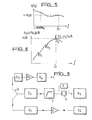
- a response curve is thus obtained, the shape of which is given in FIG. 4 where the peak f 0 has sufficient dynamics and where the insertion loss is further reduced to approximately -6 dB.
- This value results in practice from a compromise because the adaptation is not necessarily done on the inherent impedance of the quartz for reasons which will be more precisely explained in the following description.
- the gain curve of a UHF transistor mounted as a common emitter has a rise to around 100 MHz, a detrimental rise since it risks causing saturation of the loop.
- a high-pass filter F attenuating the frequencies below f 0 .
- the response curve of the oscillator has the shape of FIG. 6.
- Only the resonance peak of the frequency f 0 corresponds to an open loop gain greater than O dB.
- the gain is in fact less than 0 dB both for the frequencies below f O under the action of the high-pass filter F, and for the frequencies above f 0 by the fact that the transistor has a cut-off frequency producing an attenuation of the frequencies higher than f 0 . It goes without saying that if this attenuation produced by the transistor is not sufficient, the filter F can be completed so as to make it fulfill the function of bandpass filter centered on f 0 .
- the oscillator comprises an amplifier A which is driven at its input by an adaptation quadrupole Q 1 and its output signals drive a adaptation quadrupole Q 2 .
- the feedback loop consists of an adaptation quadrupole Q 3 downstream of Q 2 , quartz Q with its compensation network R, the high-pass filter F and an adaptation quadrupole Q 4 .
- the output of the quadrupole Q 4 attacks a power divider D, one branch of which reinjects the output signals from Q 4 to the input of Q 1 , and the other branch of which directs a fraction of the signals output from Q 4 to an amplifier output A 1 via an adaptation quadrupole Q 5 .
- the signals at the output of the output amplifier A are directed to the output S via an adaptation quadrupole Q 6 .
- the adaptation quadrupoles are line elements and / or discrete components arranged so as to carry out an impedance adaptation.
- impedance matching is a classic technique. Such an operation is carried out for example by measuring with the aid of a network analyzer the parameters (usually called parameters S) of input and output of each of the quadrupoles before their adaptation, and by calculating the element or elements of adaptation to be introduced into the quadrupole considered.
- parameters S usually called parameters of input and output of each of the quadrupoles before their adaptation
- Such calculation formulas are given in the work of P. GRIVET entitled "Physics of HF and UHF lines", Tome 2, "Circuits et amplis microwaves", edited by MASSON et Cie.
- FIG. 8 shows an example of an embodiment of the filter F in the form of a ⁇ filter comprising a variable capacitor C 2 surrounded by two reactors respectively L 2 and L 3 , one terminal of which is grounded.
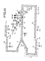
- the oscillator is made in 50 ohm micro-ribbon technology.
- the polarization of the transistors T and T has not been shown. It can be carried out as illustrated in FIG. 11.
- the amplifier A consists of a transistor T of the BFP 91 type from THOMSON-CSF. It is mounted as a common transmitter.
- the impedance matching at the input and at the output of the transistor T is carried out by a line length and a discrete component.
- the adaptation to the input of the transistor T is carried out by a line length 10 and a self-adaptation to ground L 10 .
- the line length 10 and the choke L 10 constitute the quadrupole Q of FIG. 9.
- the adaptation at the output of the transistor T is carried out by a line length 20 and a capacitor C20 to ground, constituting the quadrupole Q 2 .
- the adaptation to the input of the feedback loop is effected by a line length 30 and a ground capacitor C 30 constituting the quadrupole Q 3 .
- the adaptation is carried out by a line length 40 and a ground choke L 40 ' constituting the quadrupole Q 4 .
- each of the quadrupoles can use as an adaptation element a self or a capacity according to the results that give the measurements carried out using the network analyzer.
- the results can be such that for one or more of the quadrupoles, there is no need to implement an adaptation element.
- the length of line 40 leads to a divider D of the Wilkinson type comprising two branches forming a Y, each of branches having a length equal to ⁇ 0/4 where ⁇ 0 is the wavelength corresponding to the frequency f 0 .
- a divider can be calculated by the method indicated in the article N. Way Hybrid Power Divider, published in the review IEE Microwave N ° 1, 1969 under the signature of Ernest Wilkinson.
- One of the branches of the divider D leads to a line length 1, the length of which will be chosen so that, at the frequency f 0 , the Berkausen phase condition is respected, that is to say that the phase shift of the loop is equal to 0 modulo 2k ⁇ .
- the end of the other branch of the Wilkinson divider opens into a line 50 which drives an output transistor T l of the same type as the transistor T and also mounted as a common emitter.
- the transistor is adapted by the line length 50 to which is added a self L 50 to the ground constituting the quadrupole Q 5 , and at the output by a line length 60 and a capacitor at ground C 60 , constituting the quadrupole Q 6 .
- the end of line 60 constitutes the output S of the oscillator.
- this function can be performed using an electronic frequency tuning circuit.
- This comprises a fixed capacitor C in series in the feedback loop at the terminal of which the actual tuning circuit is connected, comprising a Varicap diode D v , the two terminals of which are connected to the terminals of the capacitor C a by l 'through two capacitors C 4 and C 5 respectively .
- the + terminal of the Varicap diode D v is connected to ground via a bias resistor R 4 .
- the terminal - of the Varicap diode D v receives a control voltage V c through a resistor R 5 .
- the control voltage V c is decoupled by a shock inductor L dl connected in series between the resistor R 5 and the variable voltage supply V c .
- a shock inductor L dl connected in series between the resistor R 5 and the variable voltage supply V c .
- the choke L dl At the terminals of the choke L dl , one of the terminals of two decoupling capacitors C dl , Cd2 are mounted, the other terminal of which is grounded.
- the variation of the capacitance value of the varicap diode D v has the effect of slightly varying the phase shift produced by the against-feedback loop. It is no longer zero modulo 2 ⁇ at the frequency f 0 , but at a frequency f ' 0 very close and located on the peak f 0 , and which therefore becomes the frequency of the oscillator. Any variation of V, for example by a potentiometric divider, causes f ' 0 to vary.
- FIG. 11 re presents an embodiment in discrete component technology.
- a matching capacitor C 21 is connected between the collector of transistor T and ground. This capacitor C 21 constitutes the adaptation element of the quadrupole Q 2 .
- the Q 3 quadrupole is adapted using a series L 31 choke and a L 32 parallel choke, one terminal of which is grounded.
- the quadrupole Q 4 is adapted using a series choke L 41 and a parallel choke L 42 , one terminal of which is grounded.
- the adaptation element of the quadrupole Q 1 at the input of the transistor T is constituted by a variable capacitor C 11 connected between the output of the coaxial line of length 1 and the ground.
- the input of the base of transistor T is decoupled by a series decoupling capacitor C d12 .
- the emitter of transistor T is charged by a resistor R 8 and decoupled by a decoupling capacitor C dl6 , connected between the emitter of T 1 and ground.
- the output signal is taken simply by means of a decoupling capacitor C d13 ', that is to say that the two transistors T and T are supplied in parallel from the output of the coaxial line of length 1 without any other precaution than the impedance adaptation of the quadrupole Q 5 carried out by a variable capacitor C 51 connected between the base of the transistor T 1 , upstream of a decoupling capacitor C d14 ' and the ground.
- the output S of transistor T 1 is adapted by a parallel choke L 61 , one terminal of which is grounded (quadrupole Q 6 ) and the direct voltages that may possibly be present at the output of the collector of transistor Q I are decoupled by a capacitor of decoupling C d15 .
- the emitter of transistor T is charged by a resistor R 11 and decoupled by a decoupling capacitor C d77 connected between the emitter of T and ground.
- the polarization of the transistors T and T 1 takes place from a voltage V decoupled in particular by a series of four cells 70 to 73 each composed of a shock inductor L d (indexed from 70 to 73) arranged in series, and a decoupling capacitor C d (indexed from 70 to 73) mounted in parallel and one terminal of which is grounded.
- the first cell 70 receives the voltage V at a first terminal of its choke L d70 , the second terminal of which is connected to one end of a resistive divider bridge R 9 , R 10 whose midpoint is connected to the base of the transistor T 1 . Between R 10 and earth, a decoupling capacitor C d76 is also connected.
- the deu- x Ie me terminal of the inductor L d70 attack a cell 71 of which the inductance L d71 is connected to the collector of the transistor T by the inductor L d75.
- the shock inductors used for decoupling have a value of 1 ⁇ H and the decoupling capacitors, a value of 1 nF.
- the values of the other elements result from the calculations indicated above, in particular as regards the impedance adaptations. Note that these depend not only on the quartz used but also on the transistor used. Even two transistors from the same series do not have exactly the same properties. Note also that a quartz resonant at 1 GHz has at this frequency a characteristic impedance (resistance R I ) of approximately 400 ⁇ .
- the invention is not limited to the embodiments described and shown.
- the order in which the elements of the feedback loop (quartz, filter and possibly electronic frequency tuning) are arranged is immaterial.
- the sampling of the output signal by a power divider which can be of any known type, can take place at any point of the loop.
- the power divider can be replaced by a directional coupler.
Landscapes
- Inductance-Capacitance Distribution Constants And Capacitance-Resistance Oscillators (AREA)
Applications Claiming Priority (2)
| Application Number | Priority Date | Filing Date | Title |
|---|---|---|---|
| FR8316384 | 1983-10-14 | ||
| FR8316384A FR2553602B1 (fr) | 1983-10-14 | 1983-10-14 | Oscillateur a quartz pour tres hautes frequences |
Publications (3)
| Publication Number | Publication Date |
|---|---|
| EP0139583A2 true EP0139583A2 (de) | 1985-05-02 |
| EP0139583A3 EP0139583A3 (en) | 1985-08-28 |
| EP0139583B1 EP0139583B1 (de) | 1988-05-04 |
Family
ID=9293146
Family Applications (1)
| Application Number | Title | Priority Date | Filing Date |
|---|---|---|---|
| EP84402015A Expired EP0139583B1 (de) | 1983-10-14 | 1984-10-08 | Quarzoszillator für sehr hohe Frequenzen |
Country Status (5)
| Country | Link |
|---|---|
| US (1) | US4646034A (de) |
| EP (1) | EP0139583B1 (de) |
| CA (1) | CA1238375A (de) |
| DE (1) | DE3470981D1 (de) |
| FR (1) | FR2553602B1 (de) |
Cited By (1)
| Publication number | Priority date | Publication date | Assignee | Title |
|---|---|---|---|---|
| FR2601529A1 (fr) * | 1986-07-09 | 1988-01-15 | Cepe | Oscillateur hyperfrequence a quartz de type transmission emetteur commun a deux transistors et a surtension en charge determinee |
Families Citing this family (4)
| Publication number | Priority date | Publication date | Assignee | Title |
|---|---|---|---|---|
| US4843349A (en) * | 1988-04-27 | 1989-06-27 | Westinghouse Electric Corp. | UHF crystal oscillator |
| US5053773A (en) * | 1989-03-15 | 1991-10-01 | Rockwell International Corporation | Doppler compensated airborne weather radar system |
| AUPQ945500A0 (en) * | 2000-08-15 | 2000-09-07 | Commonwealth Scientific And Industrial Research Organisation | Frequency adjustable oscillator and methods of operation |
| JP2004048652A (ja) * | 2002-11-29 | 2004-02-12 | Toyo Commun Equip Co Ltd | 高周波圧電発振器 |
Family Cites Families (6)
| Publication number | Priority date | Publication date | Assignee | Title |
|---|---|---|---|---|
| US2683810A (en) * | 1949-03-30 | 1954-07-13 | Marconi Wireless Telegraph Co | Piezoelectric crystal oscillator |
| FR1473273A (fr) * | 1966-02-01 | 1967-03-17 | Csf | Oscillateur à quartz à fréquence contrôlée |
| FR1475807A (fr) * | 1966-02-17 | 1967-04-07 | Thomson Houston Comp Francaise | Perfectionnements aux circuits oscillants |
| DE1541561B2 (de) * | 1966-08-11 | 1975-02-13 | Siemens Ag, 1000 Berlin Und 8000 Muenchen | Quarzgesteuerte Oszillatorschaltungsanordnung |
| US3875533A (en) * | 1973-10-15 | 1975-04-01 | Motorola Inc | Crystal controlled overtone oscillator having a rejection circuit for preventing oscillation at undesired overtones |
| US4378532A (en) * | 1979-04-02 | 1983-03-29 | Hewlett Packard Company | Oscillator mode suppression apparatus having bandpass effect |
-
1983
- 1983-10-14 FR FR8316384A patent/FR2553602B1/fr not_active Expired
-
1984
- 1984-10-08 EP EP84402015A patent/EP0139583B1/de not_active Expired
- 1984-10-08 DE DE8484402015T patent/DE3470981D1/de not_active Expired
- 1984-10-10 CA CA000465052A patent/CA1238375A/en not_active Expired
- 1984-10-11 US US06/659,891 patent/US4646034A/en not_active Expired - Fee Related
Cited By (3)
| Publication number | Priority date | Publication date | Assignee | Title |
|---|---|---|---|---|
| FR2601529A1 (fr) * | 1986-07-09 | 1988-01-15 | Cepe | Oscillateur hyperfrequence a quartz de type transmission emetteur commun a deux transistors et a surtension en charge determinee |
| EP0258076A1 (de) * | 1986-07-09 | 1988-03-02 | Compagnie D'electronique Et De Piezo-Electricite - C.E.P.E. | Mikrowellen-Quarzoszillator |
| US4743865A (en) * | 1986-07-09 | 1988-05-10 | Compagnie D'electronique Et De Piezoelectricite Cepe | Quartz-crystal microwave oscillator of the common-emitter transmission type with two transistors and a predetermined loaded Q factor |
Also Published As
| Publication number | Publication date |
|---|---|
| FR2553602B1 (fr) | 1988-06-17 |
| CA1238375A (en) | 1988-06-21 |
| EP0139583B1 (de) | 1988-05-04 |
| FR2553602A1 (fr) | 1985-04-19 |
| US4646034A (en) | 1987-02-24 |
| EP0139583A3 (en) | 1985-08-28 |
| DE3470981D1 (en) | 1988-06-09 |
Similar Documents
| Publication | Publication Date | Title |
|---|---|---|
| EP2405574B1 (de) | Vorrichtung zur Adaptation der Impedanz einer Komponente, die einen adaptierbaren Impedanzfilter auf der Basis eines Materials vom Typ Perowskit umfasst | |
| EP0012093B1 (de) | Verteilter Mikrowellenverstärker und diesen Verstärker enthaltende Verstärkervorrichtung | |
| EP0139583B1 (de) | Quarzoszillator für sehr hohe Frequenzen | |
| EP0775390B1 (de) | Gerät zum korrigieren der amplituden-/frequenzcharakteristik eines ein kabel durchlaufenden signals und entsprechender frequenzentzerrer | |
| EP0424255B1 (de) | Filtereinheit und entsprechender Filter | |
| FR2509928A1 (fr) | Reseau de transformation d'impedance pour filtre d'ondes acoustiques de surface | |
| WO2022195437A1 (fr) | Circuit de polarisation en bande de base et rf, et circuit amplificateur de puissance rf le comprenant | |
| EP0120756B1 (de) | Hochfrequenzbandpassverstärker mit einem eine anpassbare Impedanz enthaltenden Oszillator | |
| EP4214520A1 (de) | Spannungsquelle und verfahren zum kalibrieren dieser spannungsquelle | |
| WO1993000718A1 (fr) | Dispositif de filtrage coupe-bande hyperfrequence accordable | |
| WO1993008648A1 (fr) | Dispositif semi-conducteur incluant plusieurs blocs fonctionnels avec chacun une ligne de distribution de tension continue | |
| EP0273793B1 (de) | Hochselektiver Fallenkreis und Benutzung eines solchen Fallenkreises | |
| EP0372643B1 (de) | Integrierte Halbleiterschaltung mit einer Leistungsverstärkerstufe für Ultrahochfrequenz | |
| EP0347985A1 (de) | Allpasstyp-Schaltung für ultrahohe Frequenzen | |
| EP1168596A2 (de) | Mehfrequenz-Signalgeneratorgerät für Radiofrequenzen | |
| FR2601529A1 (fr) | Oscillateur hyperfrequence a quartz de type transmission emetteur commun a deux transistors et a surtension en charge determinee | |
| FR2622067A1 (fr) | Amplificateur haute frequence avec circuit de neutrodynage automatique | |
| FR2993712A1 (fr) | Resonateur hyperfrequence a saut d'impedance, notamment pour filtres hyperfrequence coupe-bande ou passe-bande | |
| EP0780973B1 (de) | Kerbfilter mit passiven Elementen | |
| EP2070192B1 (de) | Schnelles nachlauffilter | |
| FR2459582A1 (fr) | Oscillateur pour hyperfrequences stabilise, a conversion de frequence, et sa realisation a l'etat solide | |
| FR2605816A1 (fr) | Oscillateur hyperfrequence a transistor, accordable par tension et generateur hyperfrequence a large bande comportant de tels oscillateurs | |
| EP4395069A1 (de) | Ratten-race-trap und verfahren zur reduzierung des staus eines ratten-race-pumps dafür | |
| FR3144710A1 (fr) | Balun Rat-Race et procédé de réduction d'encombrement de Balun Rat-Race associé | |
| EP0360672A1 (de) | Piezoelektrisches monolithisches Filter mit modifizierter Selektivität |
Legal Events
| Date | Code | Title | Description |
|---|---|---|---|
| PUAI | Public reference made under article 153(3) epc to a published international application that has entered the european phase |
Free format text: ORIGINAL CODE: 0009012 |
|
| AK | Designated contracting states |
Designated state(s): DE GB NL SE |
|
| PUAL | Search report despatched |
Free format text: ORIGINAL CODE: 0009013 |
|
| RTI1 | Title (correction) | ||
| AK | Designated contracting states |
Designated state(s): DE GB NL SE |
|
| 17P | Request for examination filed |
Effective date: 19850912 |
|
| 17Q | First examination report despatched |
Effective date: 19860925 |
|
| GRAA | (expected) grant |
Free format text: ORIGINAL CODE: 0009210 |
|
| AK | Designated contracting states |
Kind code of ref document: B1 Designated state(s): DE GB NL SE |
|
| GBT | Gb: translation of ep patent filed (gb section 77(6)(a)/1977) | ||
| REF | Corresponds to: |
Ref document number: 3470981 Country of ref document: DE Date of ref document: 19880609 |
|
| PLBE | No opposition filed within time limit |
Free format text: ORIGINAL CODE: 0009261 |
|
| STAA | Information on the status of an ep patent application or granted ep patent |
Free format text: STATUS: NO OPPOSITION FILED WITHIN TIME LIMIT |
|
| 26N | No opposition filed | ||
| PG25 | Lapsed in a contracting state [announced via postgrant information from national office to epo] |
Ref country code: NL Effective date: 19900501 |
|
| NLV4 | Nl: lapsed or anulled due to non-payment of the annual fee | ||
| EAL | Se: european patent in force in sweden |
Ref document number: 84402015.6 |
|
| PGFP | Annual fee paid to national office [announced via postgrant information from national office to epo] |
Ref country code: GB Payment date: 19950920 Year of fee payment: 12 |
|
| PGFP | Annual fee paid to national office [announced via postgrant information from national office to epo] |
Ref country code: SE Payment date: 19950921 Year of fee payment: 12 |
|
| PGFP | Annual fee paid to national office [announced via postgrant information from national office to epo] |
Ref country code: DE Payment date: 19950923 Year of fee payment: 12 |
|
| PG25 | Lapsed in a contracting state [announced via postgrant information from national office to epo] |
Ref country code: GB Effective date: 19961008 |
|
| PG25 | Lapsed in a contracting state [announced via postgrant information from national office to epo] |
Ref country code: SE Effective date: 19961009 |
|
| GBPC | Gb: european patent ceased through non-payment of renewal fee |
Effective date: 19961008 |
|
| PG25 | Lapsed in a contracting state [announced via postgrant information from national office to epo] |
Ref country code: DE Effective date: 19970701 |
|
| EUG | Se: european patent has lapsed |
Ref document number: 84402015.6 |