EP0140413A2 - Dekodierschaltung für statischen RAM-Speicher - Google Patents
Dekodierschaltung für statischen RAM-Speicher Download PDFInfo
- Publication number
- EP0140413A2 EP0140413A2 EP84201315A EP84201315A EP0140413A2 EP 0140413 A2 EP0140413 A2 EP 0140413A2 EP 84201315 A EP84201315 A EP 84201315A EP 84201315 A EP84201315 A EP 84201315A EP 0140413 A2 EP0140413 A2 EP 0140413A2
- Authority
- EP
- European Patent Office
- Prior art keywords
- transistors
- gate
- series
- transistor
- memory
- Prior art date
- Legal status (The legal status is an assumption and is not a legal conclusion. Google has not performed a legal analysis and makes no representation as to the accuracy of the status listed.)
- Granted
Links
- 230000003068 static effect Effects 0.000 title claims abstract description 14
- 230000015654 memory Effects 0.000 claims abstract description 45
- 230000005669 field effect Effects 0.000 claims abstract description 15
- 230000000295 complement effect Effects 0.000 claims abstract description 5
- JBRZTFJDHDCESZ-UHFFFAOYSA-N AsGa Chemical compound [As]#[Ga] JBRZTFJDHDCESZ-UHFFFAOYSA-N 0.000 claims description 12
- 229910001218 Gallium arsenide Inorganic materials 0.000 claims description 11
- 238000004519 manufacturing process Methods 0.000 description 5
- 238000005516 engineering process Methods 0.000 description 4
- 230000006870 function Effects 0.000 description 3
- 239000000758 substrate Substances 0.000 description 3
- 239000003990 capacitor Substances 0.000 description 2
- 238000010586 diagram Methods 0.000 description 2
- 239000000463 material Substances 0.000 description 2
- 230000003071 parasitic effect Effects 0.000 description 2
- 238000004088 simulation Methods 0.000 description 2
- 229910017214 AsGa Inorganic materials 0.000 description 1
- 230000003213 activating effect Effects 0.000 description 1
- 238000004891 communication Methods 0.000 description 1
- 238000010276 construction Methods 0.000 description 1
- 238000007599 discharging Methods 0.000 description 1
- 230000000694 effects Effects 0.000 description 1
- 230000002349 favourable effect Effects 0.000 description 1
- 238000002513 implantation Methods 0.000 description 1
- 238000009434 installation Methods 0.000 description 1
- 230000010354 integration Effects 0.000 description 1
- 239000011159 matrix material Substances 0.000 description 1
- 229910052751 metal Inorganic materials 0.000 description 1
- 239000002184 metal Substances 0.000 description 1
- 238000000034 method Methods 0.000 description 1
- 230000010287 polarization Effects 0.000 description 1
- 230000036316 preload Effects 0.000 description 1
- 239000004065 semiconductor Substances 0.000 description 1
- 230000017105 transposition Effects 0.000 description 1
Images

Classifications
-
- G—PHYSICS
- G11—INFORMATION STORAGE
- G11C—STATIC STORES
- G11C11/00—Digital stores characterised by the use of particular electric or magnetic storage elements; Storage elements therefor
- G11C11/21—Digital stores characterised by the use of particular electric or magnetic storage elements; Storage elements therefor using electric elements
- G11C11/34—Digital stores characterised by the use of particular electric or magnetic storage elements; Storage elements therefor using electric elements using semiconductor devices
- G11C11/40—Digital stores characterised by the use of particular electric or magnetic storage elements; Storage elements therefor using electric elements using semiconductor devices using transistors
- G11C11/41—Digital stores characterised by the use of particular electric or magnetic storage elements; Storage elements therefor using electric elements using semiconductor devices using transistors forming static cells with positive feedback, i.e. cells not needing refreshing or charge regeneration, e.g. bistable multivibrator or Schmitt trigger
- G11C11/413—Auxiliary circuits, e.g. for addressing, decoding, driving, writing, sensing, timing or power reduction
- G11C11/417—Auxiliary circuits, e.g. for addressing, decoding, driving, writing, sensing, timing or power reduction for memory cells of the field-effect type
- G11C11/418—Address circuits
Definitions
- the invention relates to a decoder circuit for static RAM memory monolithically integrated, and consisting of a NOR logic gate P 1 , which is formed of a series of field effect transistors whose gates receive the n coded signals of addressing the memory or their complementary, whose sources are connected to ground and whose drains are interconnected and form the output of the NOR gate P 1 , which is connected to a supply terminal V DD1 via of a load and which is connected to the gate of a transistor of an output inverter stage.
- NOR logic gate P 1 which is formed of a series of field effect transistors whose gates receive the n coded signals of addressing the memory or their complementary, whose sources are connected to ground and whose drains are interconnected and form the output of the NOR gate P 1 , which is connected to a supply terminal V DD1 via of a load and which is connected to the gate of a transistor of an output inverter stage.
- the memory circuits almost always feel organized in the form of a network of cells which presents the structure of a matrix
- each memory cell has a unique address and can be selected by simultaneously activating the appropriate row and column.
- the data can be transmitted to the cell or extracted from the cell by a pair of lines common to all cells called BIT lines (in English BIT-LINE).
- Each elementary decoder is essentially made up of a NOR gate with n inputs, each intended to receive one of the address inputs coded in binary a 1 , a 2 ... a n , expressed in the form of a true signal or of its counting, formed before entering the decoder by an intermediate circuit (in English: ADDRESS BUFFER), so as to obtain on the output of the NOR gate, a combination of these binary digits, produced by the NOR logic function and constituting the address of a row or column.
- an intermediate circuit in English: ADDRESS BUFFER
- This NOR gate is formed of field effect transistors in gallium arsenide, with enrichment, having a pinch voltage V T ⁇ 0, that is to say not conducting as long as the voltage applied to the gate n 'is not greater than this voltage V T.
- the transistors constituting this NOR gate are mounted in parallel, their common source being connected to ground and their common drain being connected to the shorted gate-source of a desertion transistor, used as a so-called active load.
- the output signal from the NOR gate is carried on the input of an inverter stage so as to be able to have both the true output signal and of its complementary, then these signals are applied respectively to one of the two inputs of a PUSH-PULL stage.
- the inverter stage used comprises an enrichment transistor as an inverter transistor and a desertion transistor as a load.
- the PUSH-PULL stage also includes an enrichment transistor, mounted as a common source to ground, in series with a desertion transistor mounted as a common drain to the supply voltage.
- the decoder circuit for example, it is advantageous to replace the desertion transistors constituting the active charges by resistive charges, which are easier to carry out technologically.
- the object of the present invention is to provide a decoder circuit for an integrated static RAM memory, which allows faster access to the memory cell.
- the object of the present invention is further to provide a decoder circuit which is particularly simple to produce and which thus makes it possible to extend the field of production.
- a decoder circuit in accordance with the invention is remarkable in that the source of the transistor of the inverter stage is connected to the common drains of a second series of transistors, which form a second NOR gate P 2 , the common drains. forming the output of the decoder circuit and the sources of the transistors of the second series being connected to ground, in that the second series of transistors receives on its gates the n coded addressing signals and in that the first and the second series of transistors include a selection transistor, the gate of which receives the selection signal from the housing SB, this selection signal from the housing being applied to the selection transistors after application of the coded signals for addressing memories at the two NOR gates P 1 , P 2 .
- a decoder circuit for a dynamic memory is known from US Pat. No. 3,778,782.
- This circuit is formed by two NOR gates mounted in cascade. These NOR gates are combined with an AND gate and are controlled by clock signals for preload and logic operations.
- the teaching of this document does not lead to the production of a high speed decoder circuit in accordance with that of the present invention.
- the use of a decoder circuit as described by the cited document can give rise to problems which can be overcome by using the solutions proposed by US patent 3863230. These solutions lead to a circuit very far from relatively simple circuit made in accordance with the present invention.
- a preferred embodiment of the decoder circuit according to the invention is characterized in that the transistors are all of the enhancement type and in that the load of the first NOR gate P 1 is a resistive load.
- the invention finds its application in the realization of high-speed cache memories in English for mainframe computers used in the fields of astrology and metecrology, as well as for the processors of simulation simulation devices. flight allowing viewing of high resolution digital images.
- each elementary decoder takes up the distance between two rows or two columns of the memory. If the area occupied by the elementary decoder is less than the area which is thus allocated to it, the place is lost. It turns out that in the layout of this circuit using the chosen logic, the second NOR gate paired with the first fits very well without increasing the area provided for the decoder.
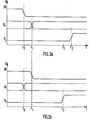
- Figures 3a and 3b show the propagation pattern of the signal V S on the word line with respect to the selection signal SB and housing relative to the signal a i selection addresses a 1, a 2 ⁇ a n, as a function of time t.
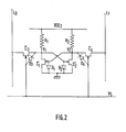
- the elementary decoder circuit comprises a first NOR gate P 1 consisting of n + 1 enhancement field effect transistors, n being the number of coded addressing signals of memory. On n of the inputs of this first NOR gate P 1 are applied the n said coded addressing signals intended to supply the combination constituting the address of a row or of a column. On the last input of this NOR gate P 1, the selection signal SB is applied.
- the charge of this NOR gate P 1 is constituted by a resistor R produced by implantation of doping materials in the GaAs substrate.
- the supply voltage VDD 1 to which this load R is connected is worth 1.2 Volt.
- the transistors of this NOR gate P 1 are mounted as a common source connected to ground.
- the output VA of the first NOR gate P 1 is done at node A, on the drains of these transistors connected to the load R, and is applied to the gate of a field effect transistor T 0 with enrichment, the drain is brought to the potential VDD 2 and the source of which is connected to the node B, to the drains of n + 1 enrichment field effect transistors mounted in parallel e + thus constituting a second NON-OR P 2 gate.
- the sources commures these transistors constituting P 2 are brought to ground.
- the voltage VDD 2 with a value of 0.7 Volt, is the supply voltage of the memory cells, as shown in FIG. 2.
- the first n inputs of this second NOR gate P 2 receive the same coded addressing signals as The first NOR gate P 1 .
- the last input of door P 2 receives the box selection signal SB.
- the output V S of the elementary decoder or line of MOT is done at node B, on the common drain of the transistors of gate P 2 .
- the output signal V S passing from 0 to 1, charges a fictitious capacitor C S.
- the "memory point" or memory cell consists of two transistors ⁇ 1 and ⁇ 2 mounted as a bistable and supplied through the resistors R 1 and R 2 respectively by the supply voltage VDD 2 . Due to the existence of fictitious diodes D 1 and D 2 , between the respective gates of these transistors and Ground, due to the fact that the transistors ⁇ 1 and ⁇ 2 are of the Schottky type, the signals V 1 and V 2 , on the drains of these latter transistors, are clipped at the value of 0.7 Volt.
- the high level or "1" of the signal V S on the line of MOT, must not exceed 0.7 Volt either, because this voltage would then be clipped by the fictitious diodes D 3 and D 4 which appear between the gate of the access transistors ⁇ 3 and ⁇ 4 , of the Schottky and Mass type, which would disturb the functioning of the memory cell, by putting these two transistors ⁇ 3 and ⁇ 4 simultaneously.
- the output signal V S is obtained, in the circuit according to the present invention, by the combination of the coded addressing signals, applied, as required, in the form, for each signal, of the true signal or of its complementary on the entrances of the NOR doors.
- the box selection signal SB is applied in a particular way to transistors equivalent to those which receive the coded addressing signals.
- FIGS. 3a and 3b there are two modes for selecting a memory point.
- the box selection signal is brought from state “1" to state "0" at time t ' 0 , while the selection a i of a combination of addresses a i , a 2 ... a n is made at time t 1 .
- the output signal V S then appears at time t ' 2 on the line of MOT, t' 2 being defined with respect to t 1 because the difference which is a function of the propagation time in the circuit and on which we cannot play.
- This time ⁇ t ' 2 constitutes the memory access time in this first operating mode.
- the signal propagation diagram is shown in Figure 3b,
- the selection a. of a combination of address a 1 , a 2 , a n is applied to the transistors T 1 , T 2 , ... T n at time t 0
- the box selection signal SB is applied to the transistor T n + 1 at time t i .
- the output signal V S then appears on the line of VOT at an instant t 2 defined by:
- the access time in memory is, in this second operating mode given by The difference:
- the circuit produced according to the invention offers the possibility of operating in this mode, which allows reduced memory access time.
- the resistors and the transistors have the following characteristics:
- the resistors e T transistors D have the following characteristics:
- the decoder circuit of this memory is composed of 2 n identical elementary decoder circuits produced according to the invention to activate the 2 n lines of the memory, and of 2 p identical elementary decoder circuits according to the invention to activate the 2 p columns of memory.
Landscapes
- Engineering & Computer Science (AREA)
- Microelectronics & Electronic Packaging (AREA)
- Computer Hardware Design (AREA)
- Static Random-Access Memory (AREA)
- Semiconductor Memories (AREA)
Applications Claiming Priority (2)
| Application Number | Priority Date | Filing Date | Title |
|---|---|---|---|
| FR8314774 | 1983-09-16 | ||
| FR8314774A FR2552257B1 (fr) | 1983-09-16 | 1983-09-16 | Circuit decodeur pour memoire ram statique |
Publications (3)
| Publication Number | Publication Date |
|---|---|
| EP0140413A2 true EP0140413A2 (de) | 1985-05-08 |
| EP0140413A3 EP0140413A3 (en) | 1985-06-12 |
| EP0140413B1 EP0140413B1 (de) | 1988-11-23 |
Family
ID=9292284
Family Applications (1)
| Application Number | Title | Priority Date | Filing Date |
|---|---|---|---|
| EP84201315A Expired EP0140413B1 (de) | 1983-09-16 | 1984-09-12 | Dekodierschaltung für statischen RAM-Speicher |
Country Status (5)
| Country | Link |
|---|---|
| US (1) | US4644189A (de) |
| EP (1) | EP0140413B1 (de) |
| JP (1) | JPS6095791A (de) |
| DE (1) | DE3475362D1 (de) |
| FR (1) | FR2552257B1 (de) |
Cited By (1)
| Publication number | Priority date | Publication date | Assignee | Title |
|---|---|---|---|---|
| FR2591789A1 (fr) * | 1985-12-17 | 1987-06-19 | Labo Electronique Physique | Circuit decodeur pour memoire ram statique |
Families Citing this family (6)
| Publication number | Priority date | Publication date | Assignee | Title |
|---|---|---|---|---|
| US4965863A (en) * | 1987-10-02 | 1990-10-23 | Cray Computer Corporation | Gallium arsenide depletion made MESFIT logic cell |
| US4885480A (en) * | 1988-08-23 | 1989-12-05 | American Telephone And Telegraph Company, At&T Bell Laboratories | Source follower field-effect logic gate (SFFL) suitable for III-V technologies |
| US4931670A (en) * | 1988-12-14 | 1990-06-05 | American Telephone And Telegraph Company | TTL and CMOS logic compatible GAAS logic family |
| US5391941A (en) * | 1993-09-23 | 1995-02-21 | Cypress Semiconductor Corporation | Decoder circuitry with balanced propagation delay and minimized input capacitance |
| US5493241A (en) * | 1994-11-16 | 1996-02-20 | Cypress Semiconductor, Inc. | Memory having a decoder with improved address hold time |
| US7821866B1 (en) | 2007-11-14 | 2010-10-26 | Cypress Semiconductor Corporation | Low impedance column multiplexer circuit and method |
Family Cites Families (8)
| Publication number | Priority date | Publication date | Assignee | Title |
|---|---|---|---|---|
| US3778782A (en) * | 1971-07-12 | 1973-12-11 | Texas Instruments Inc | Igfet dynamic address decode circuit |
| US3786277A (en) * | 1971-07-22 | 1974-01-15 | Siemens Ag | Circuit arrangement of mos transistors operating according to the dynamic principle for decoding the addresses for an mos memory |
| US3775693A (en) * | 1971-11-29 | 1973-11-27 | Moskek Co | Mosfet logic inverter for integrated circuits |
| US3863230A (en) * | 1973-07-18 | 1975-01-28 | Intel Corp | MOS memory decoder circuit |
| US4038563A (en) * | 1975-10-03 | 1977-07-26 | Mcdonnell Douglas Corporation | Symmetrical input nor/nand gate circuit |
| DE2641693C2 (de) * | 1976-09-16 | 1978-11-16 | Siemens Ag, 1000 Berlin Und 8000 Muenchen | Decodierschaltung mit MOS-Transistoren |
| JPS5826112B2 (ja) * | 1977-11-16 | 1983-05-31 | 三菱電機株式会社 | デコ−ダ回路 |
| JPS5640331A (en) * | 1979-09-11 | 1981-04-16 | Nec Corp | High-speed logical operation circuit |
-
1983
- 1983-09-16 FR FR8314774A patent/FR2552257B1/fr not_active Expired
-
1984
- 1984-09-11 US US06/649,453 patent/US4644189A/en not_active Expired - Fee Related
- 1984-09-12 EP EP84201315A patent/EP0140413B1/de not_active Expired
- 1984-09-12 DE DE8484201315T patent/DE3475362D1/de not_active Expired
- 1984-09-14 JP JP59191849A patent/JPS6095791A/ja active Granted
Cited By (2)
| Publication number | Priority date | Publication date | Assignee | Title |
|---|---|---|---|---|
| FR2591789A1 (fr) * | 1985-12-17 | 1987-06-19 | Labo Electronique Physique | Circuit decodeur pour memoire ram statique |
| EP0233383A1 (de) * | 1985-12-17 | 1987-08-26 | Laboratoires D'electronique Philips | Dekodierschaltung für einen statischen RAM-Speicher |
Also Published As
| Publication number | Publication date |
|---|---|
| FR2552257A1 (fr) | 1985-03-22 |
| JPS6095791A (ja) | 1985-05-29 |
| DE3475362D1 (en) | 1988-12-29 |
| FR2552257B1 (fr) | 1985-10-31 |
| EP0140413B1 (de) | 1988-11-23 |
| US4644189A (en) | 1987-02-17 |
| JPH0425638B2 (de) | 1992-05-01 |
| EP0140413A3 (en) | 1985-06-12 |
Similar Documents
| Publication | Publication Date | Title |
|---|---|---|
| FR2544143A1 (fr) | Reseau logique programme comportant des moyens auxiliaires de connexion au potentiel positif pour augmenter la vitesse de precharge | |
| FR2519177A1 (fr) | Dispositif a circuits integres de memoire ram dynamique | |
| FR2616934A1 (fr) | Circuit de transmission de donnees cmos dans une memoire vive dynamique | |
| EP2284839A1 (de) | Statische Speichervorrichtung mit fünf Transistoren, und entsprechendes Betriebsverfahren | |
| EP0233383B1 (de) | Dekodierschaltung für einen statischen RAM-Speicher | |
| FR2683371A1 (fr) | Memoire-tampon d'entree d'adresse d'un dispositif de memoire a semiconducteurs. | |
| EP0140413B1 (de) | Dekodierschaltung für statischen RAM-Speicher | |
| EP0237094A1 (de) | Vordiffundierte Gatterfeld-Halbleitervorrichtung für speziell hergestellte Schaltungen | |
| FR2729782A1 (fr) | Cellule de memoire a cinq transistors comportant une ligne d'alimentation en energie partagee | |
| FR2679672A1 (fr) | Circuit de transmission de donnees avec des lignes d'entree/sortie segmentees. | |
| EP3382709B1 (de) | Sram-speicherzelle | |
| EP0689713B1 (de) | Gegen kollisionen von schweren ionen unempfindliche speicherzelle | |
| FR2677162A1 (fr) | Dispositif de memoire a semiconducteurs. | |
| FR2466835A1 (fr) | Circuit rapide d'anticipation | |
| US5418748A (en) | Bit line load circuit for semiconductor static RAM | |
| US3936810A (en) | Sense line balancing circuit | |
| JPH08306189A (ja) | 内部セル電圧を減少させたsramメモリセル | |
| EP0596864A2 (de) | Verfahren zur Erhöhung der Geschwindigkeit von CMOS-Schaltungen | |
| FR2475266A1 (de) | ||
| EP0073167A1 (de) | Logischer bistabiler Schaltkreis mit Feldeffekttransistoren geringer Schwellspannung und Speichervorrichtung mit einem solchen Schaltkreis | |
| EP0897182A1 (de) | Strahlungsunempfindliche statische Speicherzelle | |
| EP0186533A1 (de) | Dynamisches Speicherelement und seine Verwendung in einer Master-Slave-Kippschaltung und in programmierbaren sequentiellen Schaltungen | |
| EP0187584A1 (de) | Logisches Koinzidenztor und dieses verwendende logische sequentielle Schaltungen | |
| US20030058718A1 (en) | Read port design and method for register array | |
| EP0003193B1 (de) | Willkürlich zugängliches statisches Speicherelement |
Legal Events
| Date | Code | Title | Description |
|---|---|---|---|
| PUAI | Public reference made under article 153(3) epc to a published international application that has entered the european phase |
Free format text: ORIGINAL CODE: 0009012 |
|
| PUAL | Search report despatched |
Free format text: ORIGINAL CODE: 0009013 |
|
| AK | Designated contracting states |
Designated state(s): DE FR GB IT NL |
|
| AK | Designated contracting states |
Designated state(s): DE FR GB IT NL |
|
| 17P | Request for examination filed |
Effective date: 19851211 |
|
| 17Q | First examination report despatched |
Effective date: 19870403 |
|
| GRAA | (expected) grant |
Free format text: ORIGINAL CODE: 0009210 |
|
| AK | Designated contracting states |
Kind code of ref document: B1 Designated state(s): DE FR GB IT NL |
|
| PG25 | Lapsed in a contracting state [announced via postgrant information from national office to epo] |
Ref country code: NL Effective date: 19881123 |
|
| REF | Corresponds to: |
Ref document number: 3475362 Country of ref document: DE Date of ref document: 19881229 |
|
| ITF | It: translation for a ep patent filed | ||
| GBT | Gb: translation of ep patent filed (gb section 77(6)(a)/1977) | ||
| NLV1 | Nl: lapsed or annulled due to failure to fulfill the requirements of art. 29p and 29m of the patents act | ||
| PLBE | No opposition filed within time limit |
Free format text: ORIGINAL CODE: 0009261 |
|
| STAA | Information on the status of an ep patent application or granted ep patent |
Free format text: STATUS: NO OPPOSITION FILED WITHIN TIME LIMIT |
|
| 26N | No opposition filed | ||
| REG | Reference to a national code |
Ref country code: FR Ref legal event code: CD |
|
| ITTA | It: last paid annual fee | ||
| PGFP | Annual fee paid to national office [announced via postgrant information from national office to epo] |
Ref country code: DE Payment date: 19951123 Year of fee payment: 12 |
|
| REG | Reference to a national code |
Ref country code: FR Ref legal event code: CJ Ref country code: FR Ref legal event code: CD |
|
| PGFP | Annual fee paid to national office [announced via postgrant information from national office to epo] |
Ref country code: GB Payment date: 19960830 Year of fee payment: 13 |
|
| PGFP | Annual fee paid to national office [announced via postgrant information from national office to epo] |
Ref country code: FR Payment date: 19960925 Year of fee payment: 13 |
|
| PG25 | Lapsed in a contracting state [announced via postgrant information from national office to epo] |
Ref country code: DE Effective date: 19970603 |
|
| PG25 | Lapsed in a contracting state [announced via postgrant information from national office to epo] |
Ref country code: GB Free format text: LAPSE BECAUSE OF NON-PAYMENT OF DUE FEES Effective date: 19970912 |
|
| PG25 | Lapsed in a contracting state [announced via postgrant information from national office to epo] |
Ref country code: FR Free format text: THE PATENT HAS BEEN ANNULLED BY A DECISION OF A NATIONAL AUTHORITY Effective date: 19970930 |
|
| GBPC | Gb: european patent ceased through non-payment of renewal fee |
Effective date: 19970912 |
|
| REG | Reference to a national code |
Ref country code: FR Ref legal event code: ST |