EP0140460B1 - Auf ISFET basierte Messanordnung und Methode zur Herstellung dieses ISFET - Google Patents
Auf ISFET basierte Messanordnung und Methode zur Herstellung dieses ISFET Download PDFInfo
- Publication number
- EP0140460B1 EP0140460B1 EP84201586A EP84201586A EP0140460B1 EP 0140460 B1 EP0140460 B1 EP 0140460B1 EP 84201586 A EP84201586 A EP 84201586A EP 84201586 A EP84201586 A EP 84201586A EP 0140460 B1 EP0140460 B1 EP 0140460B1
- Authority
- EP
- European Patent Office
- Prior art keywords
- isfet
- drift
- electrode
- source
- drain
- Prior art date
- Legal status (The legal status is an assumption and is not a legal conclusion. Google has not performed a legal analysis and makes no representation as to the accuracy of the status listed.)
- Expired
Links
Images
Classifications
-
- G—PHYSICS
- G01—MEASURING; TESTING
- G01N—INVESTIGATING OR ANALYSING MATERIALS BY DETERMINING THEIR CHEMICAL OR PHYSICAL PROPERTIES
- G01N27/00—Investigating or analysing materials by the use of electric, electrochemical, or magnetic means
- G01N27/26—Investigating or analysing materials by the use of electric, electrochemical, or magnetic means by investigating electrochemical variables; by using electrolysis or electrophoresis
- G01N27/403—Cells and electrode assemblies
- G01N27/414—Ion-sensitive or chemical field-effect transistors, i.e. ISFETS or CHEMFETS
- G01N27/4148—Integrated circuits therefor, e.g. fabricated by CMOS processing
Definitions
- the invention is related to a measuring device comprising an ISFET having a drain and a source, used as a chemically selective ion sensor, a reference electrode positioned adjacent said ISFET, an amplifier coupled to said ISFET, control circuit means coupled to said ISFET to said reference electrode and to said amplifier, adapted for maintaining two of the three operating parameters of said ISFET being the reference electrode source voltage V RS , the drain-source voltage V Ds and the drain-source current l DS constant and adjusting or measuring the third operating parameter.
- Such a measuring device comprising a chemical sensitive field effect transistor transducer is known from US-A-4 020 830.
- Said known device may be used for, for example in patients, for in vivo detection, measurement and monitoring of various chemical properties such as ion activity.
- the known device a structure is provided which includes a plurality of the said chemical selective FET transducers, each of which being adapted for simultaneously detecting and measuring different chemical properties.
- ISFET sensors such as Si 3 N 4 and AI 2 0 3 gate ISFET sensors, are highly detrimental to the accuracy and stability of measuring systems including such ISFET sensors. These drift effects restrict the applicability of such ISFET sensors, especially in the medical field.
- ISFET sensors A further drawback inherent in ISFET sensors is the long period of adjustment required when commencing a measuring procedure. As a result of such long period, acceptably stable measurements can only be performed after this period has elapsed.
- the degree of accuracy required for a biomedical pH-sensor is very high and should be at least 0.03 pH within a measuring period of a number of hours, and such accuracy preferably should be attained at the beginning of the measuring period.
- Many present-day ISFET sensors fail to fully meet these requirements as to accuracy.
- an ISFET sensor having a pH membrane/gate made of AI 2 0 3 or Si 2 N 4 or Si 3 N 4 appears to have a drift of approximately 0.02-0.06 pH/hour, and the initial drift is still far higher and may even reach values of 0.1-0.2 pH/ hour during the first hour of operation of the ISFET sensor. Accordingly, such presently available ISFET sensors are not suitable for use in the biomedical field.
- the object of the invention now is to provide a solution to the problems of drift described above.
- a measuring device of the type mentioned in the opening paragraph hereinabove characterized in that said control circuit means is incorporated in a drift correcting circuitry adapted for effecting correction of drift, due to drift effects of said ISFET on the basis of the logarithmic equation: where:
- FR-A-2 410 275 there is disclosed within the framework of looking for a solution for the known problem of signal drift a measuring device comprising an amplifier and a control circuit with a memory component.
- the control circuit effects correction of the signal drift.
- this correction is based on the slope of a straight line through two points on an experimentally determined curve while, furthermore, the known measuring device is not based on an ISFET as opposed to the device according to the invention.
- the invention is further related to an ISFET to be used as the chemically selective ion sensor in the device according to the invention including an ISFET chip, characterized in that a protective electrode is mounted on said ISFET chip adjacent an ISFET gate region, said protective electrode being electrically connected to the source or the bulk of said ISFET chip during storage; and said electrode being made of a material which has a minimal potential difference with respect to said reference electrode.
- the invention is related to a method for fabricating said ISFET to be used as the chemically selective ion sensor in the device according to the invention, said method comprising the steps of mounting a protective electrode (118) on an ISFET chip (120) adjacent an ISFET gate region (110), said electrode (118) being made of a material having minimum potential difference relative to the reference electrode (20); electrically connecting the electrode (118) to the source (122) or the bulk (124) of the ISFET so that a high DC impedance is formed in the operative range of the ISFET during operation thereof; and establishing a locally controlled electrolytic contact between the electrode (118) and the ISFET gate region (110).
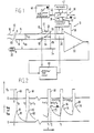
- FIG. 1 A device constructed according to the teachings of the present invention is illustrated in Fig. 1 and is generally identified by reference numeral 10.
- This device 10 was derived from empirical tests and includes circuitry which corrects for drift effects on the basis of the logarithmic equation: as defined above.
- the device 10 includes circuitry for intermittently energizing an ISFET 12 of the measuring device 10 so that its actual operating time is substantially reduced.
- the measuring device 10 includes the ISFET 12 which has a drain 14 and a source 16. Positioned adjacent the ISFET 12 in an electrolyte 18 is a reference electrode 20 which establishes a reference-source voltage V RS .
- the device 10 further includes an amplifier 22 having inputs 24 and 26 coupled respectively to the drain 14 and source 16 of the ISFET 12.
- the device 10 further includes drift correction circuitry 30 which includes a control circuit 32 that supplies a voltage to the reference electrode 20 via a conductor 34, an output 36 for controlling the gain of the amplifier 22, and input-output lines or ports 38 and 39 which are coupled to a microprocessor 40.
- drift correction circuitry 30 includes a control circuit 32 that supplies a voltage to the reference electrode 20 via a conductor 34, an output 36 for controlling the gain of the amplifier 22, and input-output lines or ports 38 and 39 which are coupled to a microprocessor 40.
- the microprocessor 40 has a memory component 42 coupled thereto, an output 44 to which a measurement signal is supplied and a duty cycle output 46 which is connected to a pulse generator 48.
- the pulse generator 48 is operable to supply a pulse 49 having a predetermined duty cycle to a sample and hold circuit 50 which, when it receives the pulse 49, samples and holds the output from the amplifier 22; and the held output is supplied via a conductor to the control circuit 32.
- the pulse 49 is supplied to two switching circuits 51 and 52 shown diagrammatically in Fig. 1.
- the switching contacts thereof are moved to positions making contact with contacts 53 and 54 connected to the drain 14 and source 16 respectively.
- the switches 51 and 52 are caused to make connection with contacts 55 and 56 which are connected to a conductor 58 connected to the conductor 34 leading to the reference electrode 20 so as to short circuit the drain 14 and source 16 with the reference electrode 20 to render the ISFET 12 inoperable during the "OFF" portion of the duty cycle.
- Fig. 2 is shown a graph of the voltage of the pulses 49 versus time superimposed over a graph of the reference-source voltage V RS versus time.
- V RS reference-source voltage
- the correction circuitry 30 connected to and forming part of the measuring device 10 includes the memory component 42 in which the logarithmic equation: and specific values of A and t are stored so that drift effects can be corrected by the microprocessor 40 utilizing the logarithmic equation.
- the device 10 can compensate for voltage drifts of V Ds or V RS over relatively short measuring periods. In such instances of short measuring periods following by a long period of stabilization, high accuracy is obtained.
- the device 10 can also be operated over a long measuring period with less high accuracy and with a circuit 32 based upon a first approximation utilizing the logarithmic equation defined above.
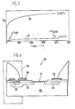
- linear correction of the voltage drift can be effected with the control circuit 32 in the measuring device 10 by first determining from a graph representing the relationship between time and drift of the voltage V Ds or V RS as shown in Fig. 3. As shown in Fig. 3, the drift for 100% duty cycle is represented by a curve 100 and the drift for a duty cycle of 10% is represented by the graph 102. In this graph the abscissa is time in seconds and the ordinate is voltage V RS , in millivolts.
- the two points found, a and b are then interconnected by a straight line and the slope of this line is entered into the memory component 42 of the correction circuitry 30.
- a correction for drift for measurements performed between one hour and four hours after actuation of the device 10 and during the time of operation of the device 10 will take place automatically on the basis of the slope stored in the memory component 42. It will be appreciated that other approximations than the linear approximation may be applied to correct the drift effects by the microprocessor 10 utilizing the logarithmic equation.
- the pulse generator 48 is provided, by which pulse excitation of the reference-source potential V RS and the drain-source potential V DS is obtained.
- Changes in voltage occurring as a result of a voltage applied across ISFET membrane or gate region 110 can be minimized by intermittently actuating the voltages respectively of the reference electrode 20 and across the drain-source terminals 14 and 16 with the period of actuation being very small over the duty cycle for the actuation pulses 49.
- the ISFET sensor 12 will exhibit drift only during the periods when the ISFET sensor 12 is energized. Then, during the "OFF" period of the duty cycle, when the measuring device is de-energized, the ISFET sensor 12 recovers from the drift effect caused by the voltages imposed thereon. In this way, the drift can be reduced by a factor that, broadly speaking, is equal to the percentage of the pulse 49 over the duty cycle of the pulses 49 and will be less than when the applied voltages V D5 and V RS are maintained continuously.
- the potential at the surface of the ISFET gate region or membrane 110 during storage is at the same potential of the reference electrode so as to provide optimal interaction of the gate region 110 with the reference electrode 20 when a measurement is made utilizing the ISFET sensor 12.
- an ISFET sensor 12 suitable for use in the measuring device 10 is constructed, according to the teachings of the present invention, with a protective electrode 118 on an ISFET chip 12 shown in Fig. 4.
- the electrode 118 is mounted on the ISFET chip 120 adjacent ISFET gate region 110.
- the electrode 118 is electrically connected to a source 122 or the bulk 124 of the chip 120.
- the bulk 124 is made of a p- Silicon material.
- the source 122 is made of a n + material as is a drain 126.
- the electrode 118 is connected through a Zener diode or avalanche diode 129 to the source 122.
- connection between the electrode 118 and the source 122 or bulk 124 has a high DC impedance in the operative range of the ISFET sensor 12 during normal operation thereof.
- the protective electrode 118 is made of a material whereby the potential difference between the protective electrode 118 and the reference electrode 20 is minimal.
- the electrode 118 is prevented from interferring with the behavior of the ISFET sensor 12 on the ISFET chip 120 during the contemplated use thereof.
- the protective electrode 118 may be directly short-circuited to the source 122 or bulk 124 by means of an external connection 140 to prevent electrical charging of the gate region 110.
- the ISFET sensor 12 and ISFET chip 120 have been described with reference to experiments made with an AI 2 0 3 gate region for the ISFET sensor 12, the device 10 is not limited to this type of ISFET sensor 12 but can be utilized in all instances where the drift phenomenon of a solid-state electronic device induced by DC voltage is incurred.
- the manufacture of the ISFET sensor 12 comprises the additional step of mounting the electrode 118 on the ISFET chip 120 adjacent the ISFET gate region 110.
- Such electrode 118 is made of a material providing a minimal potential difference relative to the reference electrode 20.
- the protective electrode 118 is electrically connected to the source 122 or the bulk 124 in such a manner that a high DC impedance is provided in the operative range of the ISFET sensor 12 during operation thereof. Further, a locally controlled electrolytic contact between the protective electrode 118 and the ISFET gate region 110 is provided.
- the EMF of various protective electrode 118 materials relative to the reference electrode 20 of the Ag/AgCI type shows that a preferred material for the protective electrode 118 is gold or silver, and preferably silver in view of its correspondence with the reference electrode 20.
- the potential difference between several electrode 118 materials and an AglAgCI reference electrode 20 as measured in a solution of electrolytes that is comparable to blood is shown in the following table.
- the EMF measurements were made at room temperature.
- the electrolytic contact between the protective electrode 118 and the gate region 110 can be controlled by contaminating the ISFET gate region 110 with a hygroscopic salt compound, particularly NaCI, such as by immersion of the ISFET sensor 12 into an NaCI solution.
- a hygroscopic salt compound particularly NaCI
- Another way of controlling the electrolytic contact is by coating the protective electrode 118 and the ISFET gate region 110 with a hydrogel such as agar-agar.
- a hydrogel such as agar-agar.
- the coating of an ISFET gate region has been proposed in European Published Patent Application 0 036 171 by Berg- veld and Koning for: Electrochemical Sensing Apparatus with in situ Calibration and Method of Making Same.
- the coating of a catheter-tip ISFET with hydrogel is disclosed in the article entitled: "Application of catheter-tip i.s.f.e.t. for continuous in vivo measurement" by Shimada, Yano and Shibatani which appeared in Volume 18, Issue No. of the Journal Medial & Biological Engineering & Computing published in 1980.
- the measuring device 10 of the present invention provides a number of advantages some of which have been described above and others of which are inherent in the invention.
Landscapes
- Chemical & Material Sciences (AREA)
- Engineering & Computer Science (AREA)
- Microelectronics & Electronic Packaging (AREA)
- Health & Medical Sciences (AREA)
- Life Sciences & Earth Sciences (AREA)
- Electrochemistry (AREA)
- Molecular Biology (AREA)
- Chemical Kinetics & Catalysis (AREA)
- Computer Hardware Design (AREA)
- Physics & Mathematics (AREA)
- Analytical Chemistry (AREA)
- Biochemistry (AREA)
- General Health & Medical Sciences (AREA)
- General Physics & Mathematics (AREA)
- Immunology (AREA)
- Pathology (AREA)
- Investigating Or Analyzing Materials By The Use Of Electric Means (AREA)
- Measurement Of The Respiration, Hearing Ability, Form, And Blood Characteristics Of Living Organisms (AREA)
Claims (14)


Applications Claiming Priority (2)
| Application Number | Priority Date | Filing Date | Title |
|---|---|---|---|
| NL8303792 | 1983-11-03 | ||
| NL8303792A NL8303792A (nl) | 1983-11-03 | 1983-11-03 | Inrichting voorzien van een op een isfet gebaseerd meetcircuit; voor toepassing in het meetcircuit geschikte isfet en werkwijze ter vervaardiging van een in het meetcircuit toe te passen isfet. |
Publications (2)
| Publication Number | Publication Date |
|---|---|
| EP0140460A1 EP0140460A1 (de) | 1985-05-08 |
| EP0140460B1 true EP0140460B1 (de) | 1989-02-08 |
Family
ID=19842655
Family Applications (1)
| Application Number | Title | Priority Date | Filing Date |
|---|---|---|---|
| EP84201586A Expired EP0140460B1 (de) | 1983-11-03 | 1984-11-02 | Auf ISFET basierte Messanordnung und Methode zur Herstellung dieses ISFET |
Country Status (6)
| Country | Link |
|---|---|
| US (1) | US4701253A (de) |
| EP (1) | EP0140460B1 (de) |
| JP (1) | JPH0765984B2 (de) |
| CA (1) | CA1237770A (de) |
| DE (1) | DE3476699D1 (de) |
| NL (1) | NL8303792A (de) |
Families Citing this family (57)
| Publication number | Priority date | Publication date | Assignee | Title |
|---|---|---|---|---|
| US4879517A (en) * | 1988-07-25 | 1989-11-07 | General Signal Corporation | Temperature compensation for potentiometrically operated ISFETS |
| EP0493626B1 (de) * | 1990-12-21 | 1994-04-13 | KNICK ELEKTRONISCHE MESSGERÄTE GMBH & CO. | Ausgangsschaltung zur analogen Ausgabe eines in Bezug auf Steilheit und Nullpunkt kompensierten Messsignals und Verfahren zum Ausgeben des Messsignals |
| US5317275A (en) * | 1992-01-13 | 1994-05-31 | Orbital Sciences Corporation | Conductance measurement circuit with wide dynamic range |
| JP2541081B2 (ja) * | 1992-08-28 | 1996-10-09 | 日本電気株式会社 | バイオセンサ及びバイオセンサの製造・使用方法 |
| WO1994026029A1 (en) * | 1993-04-26 | 1994-11-10 | Unifet Incorporated | Method and apparatus for multiplexing devices having long thermal time constants |
| US5911873A (en) * | 1997-05-02 | 1999-06-15 | Rosemount Analytical Inc. | Apparatus and method for operating an ISFET at multiple drain currents and gate-source voltages allowing for diagnostics and control of isopotential points |
| SE9703957D0 (sv) | 1997-10-29 | 1997-10-29 | Pacesetter Ab | Method and device for sensing |
| SE9703958D0 (sv) * | 1997-10-29 | 1997-10-29 | Pacesetter Ab | Method and device for determination of concentration |
| DE19857953C2 (de) * | 1998-12-16 | 2001-02-15 | Conducta Endress & Hauser | Vorrichtung zum Messen der Konzentration von Ionen in einer Meßflüssigkeit |
| DE10151020A1 (de) * | 2001-10-16 | 2003-04-30 | Infineon Technologies Ag | Schaltkreis-Anordnung, Sensor-Array und Biosensor-Array |
| US7232512B2 (en) * | 2004-08-25 | 2007-06-19 | Honeywell International, Inc. | System and method of sensitivity adjustment for an electrochemical sensor |
| CN100446417C (zh) * | 2004-12-23 | 2008-12-24 | 中国科学院电子学研究所 | 基于双模式的集成isfet传感器信号差分读出电路 |
| TWI296709B (en) * | 2005-10-21 | 2008-05-11 | Univ Chung Yuan Christian | Ion sensing circuit with body effect reduction technique |
| US7581390B2 (en) * | 2006-04-26 | 2009-09-01 | Cummins Inc. | Method and system for improving sensor accuracy |
| CN101101272B (zh) * | 2006-07-07 | 2010-10-13 | 中国科学院电子学研究所 | 一种生化微传感集成芯片、制作及模具制备方法 |
| US8349167B2 (en) | 2006-12-14 | 2013-01-08 | Life Technologies Corporation | Methods and apparatus for detecting molecular interactions using FET arrays |
| GB2457851B (en) | 2006-12-14 | 2011-01-05 | Ion Torrent Systems Inc | Methods and apparatus for measuring analytes using large scale fet arrays |
| US11339430B2 (en) | 2007-07-10 | 2022-05-24 | Life Technologies Corporation | Methods and apparatus for measuring analytes using large scale FET arrays |
| US8262900B2 (en) | 2006-12-14 | 2012-09-11 | Life Technologies Corporation | Methods and apparatus for measuring analytes using large scale FET arrays |
| JP5123316B2 (ja) * | 2007-01-04 | 2013-01-23 | コーニンクレッカ フィリップス エレクトロニクス エヌ ヴィ | サンプル濃度を測定する方法、検出器及びシステム |
| JP5056398B2 (ja) * | 2007-12-19 | 2012-10-24 | 株式会社豊田中央研究所 | センサの使用方法及びセンサ装置 |
| EP2307577B1 (de) | 2008-06-25 | 2015-06-03 | Life Technologies Corporation | Verfahren zur analytmessung mithilfe grosser fet-arrays |
| US20100301398A1 (en) | 2009-05-29 | 2010-12-02 | Ion Torrent Systems Incorporated | Methods and apparatus for measuring analytes |
| US20100137143A1 (en) | 2008-10-22 | 2010-06-03 | Ion Torrent Systems Incorporated | Methods and apparatus for measuring analytes |
| US8776573B2 (en) | 2009-05-29 | 2014-07-15 | Life Technologies Corporation | Methods and apparatus for measuring analytes |
| US20120261274A1 (en) | 2009-05-29 | 2012-10-18 | Life Technologies Corporation | Methods and apparatus for measuring analytes |
| TWI465716B (zh) | 2010-06-30 | 2014-12-21 | 生命技術公司 | 用於檢測及測量化學反應及化合物之電晶體電路 |
| EP2588851B1 (de) | 2010-06-30 | 2016-12-21 | Life Technologies Corporation | Ion-sensing charge-accumulation circuit and method |
| US11307166B2 (en) | 2010-07-01 | 2022-04-19 | Life Technologies Corporation | Column ADC |
| US8653567B2 (en) | 2010-07-03 | 2014-02-18 | Life Technologies Corporation | Chemically sensitive sensor with lightly doped drains |
| DE102010040264A1 (de) * | 2010-09-03 | 2012-03-08 | Endress + Hauser Conducta Gesellschaft für Mess- und Regeltechnik mbH + Co. KG | Verfahren zur Bestimmung der Ionenkonzentration oder zur Bestimmung einer Stoffkonzentration in einer Lösung |
| WO2012036679A1 (en) | 2010-09-15 | 2012-03-22 | Life Technologies Corporation | Methods and apparatus for measuring analytes |
| US8685324B2 (en) | 2010-09-24 | 2014-04-01 | Life Technologies Corporation | Matched pair transistor circuits |
| US9970984B2 (en) | 2011-12-01 | 2018-05-15 | Life Technologies Corporation | Method and apparatus for identifying defects in a chemical sensor array |
| US8821798B2 (en) | 2012-01-19 | 2014-09-02 | Life Technologies Corporation | Titanium nitride as sensing layer for microwell structure |
| US8747748B2 (en) | 2012-01-19 | 2014-06-10 | Life Technologies Corporation | Chemical sensor with conductive cup-shaped sensor surface |
| US8786331B2 (en) | 2012-05-29 | 2014-07-22 | Life Technologies Corporation | System for reducing noise in a chemical sensor array |
| US9080968B2 (en) | 2013-01-04 | 2015-07-14 | Life Technologies Corporation | Methods and systems for point of use removal of sacrificial material |
| US9841398B2 (en) | 2013-01-08 | 2017-12-12 | Life Technologies Corporation | Methods for manufacturing well structures for low-noise chemical sensors |
| US8962366B2 (en) | 2013-01-28 | 2015-02-24 | Life Technologies Corporation | Self-aligned well structures for low-noise chemical sensors |
| US8963216B2 (en) | 2013-03-13 | 2015-02-24 | Life Technologies Corporation | Chemical sensor with sidewall spacer sensor surface |
| US8841217B1 (en) | 2013-03-13 | 2014-09-23 | Life Technologies Corporation | Chemical sensor with protruded sensor surface |
| US9116117B2 (en) | 2013-03-15 | 2015-08-25 | Life Technologies Corporation | Chemical sensor with sidewall sensor surface |
| WO2014149779A1 (en) | 2013-03-15 | 2014-09-25 | Life Technologies Corporation | Chemical device with thin conductive element |
| EP2972279B1 (de) | 2013-03-15 | 2021-10-06 | Life Technologies Corporation | Chemischer sensor mit stetigen sensoroberflächen |
| US9835585B2 (en) | 2013-03-15 | 2017-12-05 | Life Technologies Corporation | Chemical sensor with protruded sensor surface |
| CN105264366B (zh) | 2013-03-15 | 2019-04-16 | 生命科技公司 | 具有一致传感器表面区域的化学传感器 |
| US20140336063A1 (en) | 2013-05-09 | 2014-11-13 | Life Technologies Corporation | Windowed Sequencing |
| US10458942B2 (en) | 2013-06-10 | 2019-10-29 | Life Technologies Corporation | Chemical sensor array having multiple sensors per well |
| US9281219B2 (en) | 2013-09-18 | 2016-03-08 | Suprasensor Technologies, Llc | Molecular receptor-based chemical field-effect transistor (CHEMFET) devices, systems, and methods for in-situ nitrate monitoring in field soils |
| WO2016100521A1 (en) | 2014-12-18 | 2016-06-23 | Life Technologies Corporation | Methods and apparatus for measuring analytes using large scale fet arrays |
| KR102593647B1 (ko) | 2014-12-18 | 2023-10-26 | 라이프 테크놀로지스 코포레이션 | 트랜스미터 구성을 갖춘 높은 데이터율 집적 회로 |
| US10077472B2 (en) | 2014-12-18 | 2018-09-18 | Life Technologies Corporation | High data rate integrated circuit with power management |
| JP7088541B2 (ja) * | 2018-05-24 | 2022-06-21 | ラピスセミコンダクタ株式会社 | 測定装置及び測定方法 |
| MX2021003289A (es) | 2018-09-21 | 2021-08-11 | Teralytic Holdings Inc | Plataforma de fusión de sensor multimodal extensible, para deteccion de terreno proximal, remota. |
| DE102021133958A1 (de) | 2021-12-21 | 2023-06-22 | Endress+Hauser Conducta Gmbh+Co. Kg | Verfahren zum Kalibrieren einer Messschaltung, Messschaltung für einen elektrochemischen Sensor |
| DE102023000854A1 (de) * | 2022-03-02 | 2023-09-07 | Technische Universität Ilmenau, Körperschaft des öffentlichen Rechts | Verfahren zur störungsreduzierten Messung und/oder Überwachung des pH-Wertes eines Mediums und dazugehörige Vorrichtung |
Citations (1)
| Publication number | Priority date | Publication date | Assignee | Title |
|---|---|---|---|---|
| US4020830A (en) * | 1975-03-12 | 1977-05-03 | The University Of Utah | Selective chemical sensitive FET transducers |
Family Cites Families (12)
| Publication number | Priority date | Publication date | Assignee | Title |
|---|---|---|---|---|
| DE1919406C3 (de) * | 1968-04-23 | 1981-11-05 | Naamloze Vennootschap Philips' Gloeilampenfabrieken, Eindhoven | Feldeffekttransistor und seine Verwendung in einer Schaltungsanordnung für einen Miller-Integrator |
| US4207146A (en) * | 1977-01-12 | 1980-06-10 | Dragerwerk Aktiengesellschaft | Process for testing gases in body fluids for partial pressure and to a testing device therefor |
| US4273636A (en) * | 1977-05-26 | 1981-06-16 | Kiyoo Shimada | Selective chemical sensitive field effect transistor transducers |
| JPS5459199A (en) * | 1977-10-20 | 1979-05-12 | Olympus Optical Co Ltd | Ion concentration measuring apparatus |
| FR2410275A1 (fr) * | 1977-11-28 | 1979-06-22 | Claude Bernard | Dispositif de calibration automatique d'appareils tels que phmetres, ionometres, appareils de mesure de potentiels d'electrodes |
| DE2917714C2 (de) * | 1979-05-02 | 1983-12-22 | Degussa Ag, 6000 Frankfurt | Verfahren zur Messung mit Redox- oder ionensensitiven Elektroden |
| US4269684A (en) * | 1979-10-01 | 1981-05-26 | Cordis Corporation | Apparatus for oxygen partial pressure measurement |
| US4384925A (en) * | 1980-10-24 | 1983-05-24 | Becton Dickinson And Company | Gas sensing unit with automatic calibration method |
| DE3047782A1 (de) * | 1980-12-18 | 1982-07-08 | Drägerwerk AG, 2400 Lübeck | Schaltungsanordnung zur korrektur der sensorausgangsgroesse |
| EP0074498B1 (de) * | 1981-09-04 | 1985-12-04 | F. HOFFMANN-LA ROCHE & CO. Aktiengesellschaft | Verfahren und Vorrichtung zum Eichen von Messfühlern |
| US4411741A (en) * | 1982-01-12 | 1983-10-25 | University Of Utah | Apparatus and method for measuring the concentration of components in fluids |
| US4488556A (en) * | 1982-06-03 | 1984-12-18 | Critikon, Inc. | AC Mode operation of chemfet devices |
-
1983
- 1983-11-03 NL NL8303792A patent/NL8303792A/nl not_active Application Discontinuation
-
1984
- 1984-10-29 US US06/665,808 patent/US4701253A/en not_active Expired - Fee Related
- 1984-11-01 CA CA000466881A patent/CA1237770A/en not_active Expired
- 1984-11-02 DE DE8484201586T patent/DE3476699D1/de not_active Expired
- 1984-11-02 EP EP84201586A patent/EP0140460B1/de not_active Expired
- 1984-11-02 JP JP59230518A patent/JPH0765984B2/ja not_active Expired - Lifetime
Patent Citations (2)
| Publication number | Priority date | Publication date | Assignee | Title |
|---|---|---|---|---|
| US4020830A (en) * | 1975-03-12 | 1977-05-03 | The University Of Utah | Selective chemical sensitive FET transducers |
| US4020830B1 (de) * | 1975-03-12 | 1984-09-04 |
Also Published As
| Publication number | Publication date |
|---|---|
| CA1237770A (en) | 1988-06-07 |
| NL8303792A (nl) | 1985-06-03 |
| US4701253A (en) | 1987-10-20 |
| JPS60113143A (ja) | 1985-06-19 |
| EP0140460A1 (de) | 1985-05-08 |
| DE3476699D1 (en) | 1989-03-16 |
| JPH0765984B2 (ja) | 1995-07-19 |
Similar Documents
| Publication | Publication Date | Title |
|---|---|---|
| EP0140460B1 (de) | Auf ISFET basierte Messanordnung und Methode zur Herstellung dieses ISFET | |
| US5217595A (en) | Electrochemical gas sensor | |
| US5911873A (en) | Apparatus and method for operating an ISFET at multiple drain currents and gate-source voltages allowing for diagnostics and control of isopotential points | |
| US4641084A (en) | Ion concentration measuring apparatus | |
| US4627906A (en) | Electrochemical sensor having improved stability | |
| US4851104A (en) | Instrument for potentiometric electrochemical measurements | |
| EP0146977A1 (de) | Vorrichtung zur Bestimmung der Aktivität eines Ions (Pion) in einer Flüssigkeit | |
| US7323091B1 (en) | Multimode electrochemical sensing array | |
| US10900929B2 (en) | PH value measuring device comprising in situ calibration means | |
| JPS5824851A (ja) | イオン濃度を測定する方法および装置 | |
| EP0231609A3 (de) | Leitfähigkeitssensor für reines Wasser | |
| GB2077439A (en) | Compensating temperature-dependent characteristic changes in ion-sensitive fet transducers | |
| EP0352537B1 (de) | Temperaturausgleich für potentiometrisch arbeitende ISFETs | |
| US3652439A (en) | Appratus for measuring ph in high-pressure environments | |
| US4457808A (en) | Method and means for recalibrating electrochemical cells in situ | |
| US4589970A (en) | Apparatus for selectively measuring ions in a liquid | |
| EP0139312B1 (de) | Vorrichtung zur selektiven Messung von Ionen in einer Flüssigkeit | |
| US20070084721A1 (en) | Drift calibration method and device for the potentiometric sensor | |
| US11041824B2 (en) | Measurement device and measurement method | |
| US11280754B2 (en) | Measuring probe for electrochemical measurements | |
| EP0155725A1 (de) | Vorrichtung zur Messung einer ionischen Konzentration mittels eines Messfeldeffekttransistors und eines Referenzfeldeffekttransistors, die beide für dasselbe Ion empfindlich sind | |
| WO1999022232A8 (en) | Method and device for sensing | |
| US4459180A (en) | Method and means for compensating for IR voltage drop in electrochemical cells | |
| KR910006276B1 (ko) | 감이온 전계효과 트랜지스터를 이용한 이온농도 측정 회로 | |
| EP0280230A2 (de) | Gerät zur Messung von elektrochemischen Potentialen in/an einer Elektrolytlösung |
Legal Events
| Date | Code | Title | Description |
|---|---|---|---|
| PUAI | Public reference made under article 153(3) epc to a published international application that has entered the european phase |
Free format text: ORIGINAL CODE: 0009012 |
|
| AK | Designated contracting states |
Designated state(s): DE FR GB IT NL |
|
| 17P | Request for examination filed |
Effective date: 19850617 |
|
| 17Q | First examination report despatched |
Effective date: 19861016 |
|
| D17Q | First examination report despatched (deleted) | ||
| RAP1 | Party data changed (applicant data changed or rights of an application transferred) |
Owner name: SENTRON V.O.F. |
|
| GRAA | (expected) grant |
Free format text: ORIGINAL CODE: 0009210 |
|
| AK | Designated contracting states |
Kind code of ref document: B1 Designated state(s): DE FR GB IT NL |
|
| PG25 | Lapsed in a contracting state [announced via postgrant information from national office to epo] |
Ref country code: NL Effective date: 19890208 Ref country code: IT Free format text: LAPSE BECAUSE OF FAILURE TO SUBMIT A TRANSLATION OF THE DESCRIPTION OR TO PAY THE FEE WITHIN THE PRESCRIBED TIME-LIMIT;WARNING: LAPSES OF ITALIAN PATENTS WITH EFFECTIVE DATE BEFORE 2007 MAY HAVE OCCURRED AT ANY TIME BEFORE 2007. THE CORRECT EFFECTIVE DATE MAY BE DIFFERENT FROM THE ONE RECORDED. Effective date: 19890208 Ref country code: FR Free format text: THE PATENT HAS BEEN ANNULLED BY A DECISION OF A NATIONAL AUTHORITY Effective date: 19890208 |
|
| REF | Corresponds to: |
Ref document number: 3476699 Country of ref document: DE Date of ref document: 19890316 |
|
| EN | Fr: translation not filed | ||
| NLV1 | Nl: lapsed or annulled due to failure to fulfill the requirements of art. 29p and 29m of the patents act | ||
| PLBE | No opposition filed within time limit |
Free format text: ORIGINAL CODE: 0009261 |
|
| STAA | Information on the status of an ep patent application or granted ep patent |
Free format text: STATUS: NO OPPOSITION FILED WITHIN TIME LIMIT |
|
| 26N | No opposition filed | ||
| PGFP | Annual fee paid to national office [announced via postgrant information from national office to epo] |
Ref country code: GB Payment date: 19921026 Year of fee payment: 9 |
|
| PGFP | Annual fee paid to national office [announced via postgrant information from national office to epo] |
Ref country code: DE Payment date: 19930113 Year of fee payment: 9 |
|
| PG25 | Lapsed in a contracting state [announced via postgrant information from national office to epo] |
Ref country code: GB Effective date: 19931102 |
|
| GBPC | Gb: european patent ceased through non-payment of renewal fee |
Effective date: 19931102 |
|
| PG25 | Lapsed in a contracting state [announced via postgrant information from national office to epo] |
Ref country code: DE Effective date: 19940802 |