EP0141486B1 - Bildsensor - Google Patents
Bildsensor Download PDFInfo
- Publication number
- EP0141486B1 EP0141486B1 EP84303897A EP84303897A EP0141486B1 EP 0141486 B1 EP0141486 B1 EP 0141486B1 EP 84303897 A EP84303897 A EP 84303897A EP 84303897 A EP84303897 A EP 84303897A EP 0141486 B1 EP0141486 B1 EP 0141486B1
- Authority
- EP
- European Patent Office
- Prior art keywords
- current
- signal
- array
- control signal
- transistors
- Prior art date
- Legal status (The legal status is an assumption and is not a legal conclusion. Google has not performed a legal analysis and makes no representation as to the accuracy of the status listed.)
- Expired - Lifetime
Links
- 238000003491 array Methods 0.000 claims description 24
- 230000003287 optical effect Effects 0.000 claims description 8
- 238000010586 diagram Methods 0.000 description 10
- 238000006243 chemical reaction Methods 0.000 description 7
- 238000000034 method Methods 0.000 description 5
- XUIMIQQOPSSXEZ-UHFFFAOYSA-N Silicon Chemical compound [Si] XUIMIQQOPSSXEZ-UHFFFAOYSA-N 0.000 description 3
- 229910052710 silicon Inorganic materials 0.000 description 3
- 239000010703 silicon Substances 0.000 description 3
- 229910021417 amorphous silicon Inorganic materials 0.000 description 2
- 230000002950 deficient Effects 0.000 description 2
- 239000000758 substrate Substances 0.000 description 2
- 239000000872 buffer Substances 0.000 description 1
- 239000002800 charge carrier Substances 0.000 description 1
- 239000002131 composite material Substances 0.000 description 1
- 239000013078 crystal Substances 0.000 description 1
- 238000001514 detection method Methods 0.000 description 1
- 230000009699 differential effect Effects 0.000 description 1
- 230000010354 integration Effects 0.000 description 1
- 229910044991 metal oxide Inorganic materials 0.000 description 1
- 150000004706 metal oxides Chemical class 0.000 description 1
- 230000002265 prevention Effects 0.000 description 1
- 230000005855 radiation Effects 0.000 description 1
- 230000008707 rearrangement Effects 0.000 description 1
- 229920006395 saturated elastomer Polymers 0.000 description 1
- 239000004065 semiconductor Substances 0.000 description 1
- 230000035945 sensitivity Effects 0.000 description 1
Images



Classifications
-
- H—ELECTRICITY
- H04—ELECTRIC COMMUNICATION TECHNIQUE
- H04N—PICTORIAL COMMUNICATION, e.g. TELEVISION
- H04N25/00—Circuitry of solid-state image sensors [SSIS]; Control thereof
- H04N25/70—SSIS architectures; Circuits associated therewith
- H04N25/701—Line sensors
Definitions
- This invention relates to a linear image sensor and more particularly to an elongate integrated image sensor used for an original read scanner or the like in order to read image-formation on the sensor, isometric to the original.
- Image sensors have previously been proposed using integrated circuit techniques and formed on silicon crystals. Such sensors include a charge-coupled device (CCD) image sensor and a metal oxide semiconductor (MOS) image sensor.
- CCD charge-coupled device
- MOS metal oxide semiconductor
- the image sensor comprises a plurality of photo-detecting elements and scanning circuits, the CCD image sensor using a photodiode for the detecting element and a charge coupled device for the scanning circuit, and the MOS image sensor using a photodiode for the detecting element and a shift register of MOS transistor for the scanning circuit.
- a CCD image sensor which uses, as the signal medium, charge carriers essentially in thermal non-equilibrium condition, has an increased dark signal at a high temperature. Also, when reading contracted image-formation, the potential well size of CCD is small (7 to 14 ⁇ m) to enable high speed scanning, but when reading isometric image, the necessary potential well size is larger (62 to 125 ⁇ m) which results in low speed scanning and, in turn, a low speed read-out.
- a MOS image sensor which has high resolution has a low scanning speed due to the limit in the maximum clock frequency of MOS shift register and also its video signal is weak and the scanning digital signal interferes intensively with the video signal line, resulting in a poor signal-to-noise ratio.
- a contact type image sensor to read images isometric to the original which has a relatively larger element pitch (for example, pitch: 62.5 ⁇ m at a resolution of 16 dots/mm and pitch: 125 ⁇ m at that of 8 dots/mm) and needs a length corresponding to a width of the original.
- element pitch for example, pitch: 62.5 ⁇ m at a resolution of 16 dots/mm and pitch: 125 ⁇ m at that of 8 dots/mm
- an amorphous silicon image sensor whose photo-detecting units are integrally elongate and a large number of driving LSI chips are mounted therearound, and a CCD multi-chip image sensor which mounts a plurality of CCD image sensors in a zigzag pattern on a substrate.
- the amorphous silicon image sensor whose detecting units are separate from driving units, has many connecting wires which results in low or uncertain reliability, and the CCD multichip image sensor is defective in that rearrangement of lines after read-out is required due to the zigzag arrangement, the transfer speed drops due to its large potential well size, and a capacity load of driving circuit increases.
- An object of the invention is to provide an image sensor of self-scanning type which has detecting units and scanning units on the same silicon chip and reads the original information optically at high speed, with high sensitivity and high resolution.
- the image sensor of the invention is preferably optimised especially for a contact type image sensor to read images isometric to the original information.
- the present invention provides a self scanning type image sensor for converting an optical signal to an electric signal comprising: a phototransistor array composed of a plurality of phototransistors for converting an optical signal to an electric current signal; a first current switch array composed of a plurality of current switches which are connected with said plurality of phototransistors respectively; a plurality of decoder circuits, each for selecting one of said plurality of current switches of said first current switch array according to a first control signal applied in common to the plurality of decoder circuits, the outputs of the plurality of decoder circuits corresponding with the current switches of the first current switch array; a second current switch array composed of a plurality of current switches for selecting one of said plurality of decoder circuits according to a second control signal; a current source circuit for supplying a current to said selected one of said plurality of decoder circuits through selected one of said plurality a drive circuit for producing said first control signal applied to each of said plurality of decoder circuits and said second control signal
- Each of said plurality of decoder circuits comprises a plurality of stages of current switch arrays composed of a plurality of dendrically connected current changeover switches each having a common input terminal, two output terminals and two control terminals corresponding to said two output terminals; the first stage of said plurality of stages of current switch arrays comprising a single current changeover switch connected at its common input terminal with one of said plurality of current switches of said second current switch array; the two output terminals of each of said plurality of current changeover switches of the last stages of said plurality of stages of current switch arrays being connected with two of said plurality of current switches of said first current switch array respectively; each of said plurality of current changeover switches of the other stages of said plurality of stages of current switch arrays being connected at its common input terminal with an output terminal of one of said plurality of current changeover switches of the previous stage and at its two output terminals with the common input terminals of two of said plurality of current changeover switches of the next stage thereby to be connected dendrically, and wherein said first
- the image sensor chip is limited in length by the size of silicon wafer (about 4 to 6 in. in diameter) and the yield of chip, thereby being about 30 to 70 mm long.
- the elongate image sensor to meet width of original needs a plurality of chips mounted on the substrate, for example, eight chips are required to constitute the contact type image sensor for reading a letter-size original by use of chip of 28 mm in effective sensing length.
- a scanning circuit comprises a plurality of decoder circuits, an input signal converter circuit for driving the decoder circuit, and a current source for the decoder circuit.
- An external selecting input signal (signal to assign a reading phototransistor) assign a current flow in any output terminal at any decoder.
- the circuits all operate in the current mode, the respective decoder circuits comprising current switching circuits dendritically connected. Since amplitude of signal to operate these current switches is small by about 0.5V and each transistor operates in active condition, the high speed scanning is possible.
- the current switches are connected so that they operate, as in Gray code, by the changing one bit number at each scanning step.
- the decoder circuit is adapted to scan with the signal changing only 1 bit when scanning the adjacent phototransistor.
- Access circuits for the phototransistors and video signal output circuits comprise current switches which turn on or off according to whether or not the current output from the respective decoder circuits, and circuits for connecting the output terminal at each current switch to one terminal of each phototransistor, the other terminal thereof connected in common being the video output terminal.
- the photocurrent signal obtained at video output terminal is converted into voltage signal by an operational amplifier.
- the main video signal is developed at a timing of turning on of the switching transistor to recharge the electric charge in the phototransistor discharged by the photocurrent.
- a second embodiment of the invention is provided with a second phototransistor array light-shielded and paired with the first detecting phototransistor array so that the second phototransistor array is connected to have access at every pair with the detecting phototransistor, and the leakage current are output from the common connecting line for second phototransistor.
- an output amplifier such as an operational amplifier, can give its differential output to thereby enable the leakage current to be canceled.
- this circuit can cancel not only the leakage current but also noises caused by interferences of the scanning digital to the video signal output line, thereby enabling the noises to be largely reduced.
- the leakage current and noise reduced by the differential effect can provide an image sensor of reduced dark output and noise output and of enlarged dynamic range.
- Still another object of the invention is to provide a driving circuit for the image sensor.
- the driving circuit comprises, a timing control circuit, a counter, code change circuit, and a block signal generator.
- the image sensor of the invention can be manufactured with the technique as to the bipolar integrated circuit and provide a novel circuitry of the image sensor.
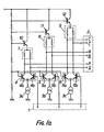
- FIG. 1-a an input signal conversion circuit (in a case of 3 bits) at an image sensor of the invention. Decoder circuits (of 16 bits output) and detecting element units of the invention are shown in Fig. 1-b.
- the input signal conversion circuit in Fig. 1-a receives the selecting input signals at input terminals 1 to convert the signals into double-ended-balanced signals different in a DC level. Currents from current sources 3a, 3b and 3c are switched by transistor pairs 4, 5 and 6 constituting current switches which conducts current toward the transistor 4a or 4b, 5a or 5b, or 6a or 6b, according to the result of comparison of selecting input signal with logic threshold voltage V th .
- the output currents from the current switches, resistance pairs 7, 8 and 9, and DC level setting transistors 10, 11 and 12, give converted signal output terminals 2 the double-ended-balanced signals different in the DC level, the signal amplitude being small by about 0.5V and less affecting the video output line, the transistor pairs 4, 5 and 6 being operable at high speed because of operation in non-saturation condition.
- the double-ended-balanced signals are received by input terminals 13 and the block selecting input signals by input terminals 14 and 15 respectively so that a current from a current source 16 and selected by the block selecting input signal is led to the branches selected by the double-ended-balanced signals and then phototransistors connected to the branches are allowed to have access, in other words, they are put into the reading condition.
- the above circuit in Fig. 1-b comprises current switch groups connected dendritically with each other. Transistors 17 and 18 together with a transistor 58 comprise current switches operating through the block selecting signals.
- Transistor pairs 19, 20, 21, 22, 23, 24 and 25 are connected as current switches for switching, according to the double-ended-balanced signals , and currents given to the emitters at each transistor pair and constitute a first decoder operating in the current mode.
- the current from the current source selected by the block selecting input signal flows into the branches selected by the double-ended-balanced signals, through the current switches connected dendritically to thereby generate a potential difference at one of load resistances 26a, 26b, 27a, 27b, 28a, 28b, 29a and 29b.
- PNP transistors 30a, 30b, 31a, 31b, 32a, 32b, 33a and 33b are switching transistors turned on or off according to whether or not the potential difference exists at both ends of each load resistance, the collectors of which are connected to a positive power source, the bases to one end of load resistance, and the emitters to the collectors of phototransistors 34a, 34b, 35a, 35b, 36a, 36b, 37a and 37b respectively.
- Reference numeral 38 designates a video output line connecting in common the emitters of the phototransistors 34a through 37b.
- the storage charge is given to the phototransistors to develop recharge and a auxiliary video signal appears on the video output line 38 to be mixed with a main video signal from next phototransistor,thereby substantially lowering the resolution.
- the collectors larger in capacity than the bases are connected to the positive power source and the emitters smaller in that than the same are connected to the collector of the phototransistors, whereby the storage charges are reducible, thus enabling the auxiliary video signal to be reduced to a minimum.
- the emitters at the phototransistors are connected in common to form a video output terminal.
- Transistor pairs 39, 40, 41, 42, 43, 44 and 45 constitute a second decoder operating in the current mode as the same as the transistor pairs 19, 20, 21, 22, 23, 24 and 25.
- reference numerals 46a, 46b, 47a, 47b, 48a, 48b, 49a and 49b designate load resistances
- 50a, 50b, 51a, 51b, 52a, 52b, 53a and 53b designate switching PNP transistors on or off according to whether or not the potential difference exists across both ends at each load resistance
- 54a, 54b, 55a, 55b, 56a, 56b, 57a and 57b designate detecting phototransistors respectively, the connections thereof being the same as the left half in the block diagram in Fig. 1-b as above-mentioned.
- the block input terminal 14 When the block input terminal 14 is at a H (high) level, that 15 is at a L (low) level, and the double-ended-balanced input signals A, B and C all are at the L level, the current from the current source flows in the resistance 26a only but not in other load resistances. As a result, the PNP transistor 30a lowers in its base potential and turn on so that a charging current flows only in the phototransistor 34a, which is put in a reading (access) condition. No current flows in other phototransistors so that they are put in the integration (non-access) period in the charge storage mode. Thus, the block selecting input signal or double-ended-balanced input signal is changed to put a desired phototransistor in the read condition, thereby enabling its photoelectric conversion signal, i.e., video signal, to be fetched.
- the photoelectric conversion signal i.e., video signal
- reference numerals 59, 60, 61 and 62 designate decoders at groups of current siwtches of 6 bits input- 64 bits output, which allow a current from the current source 65 to flow in one of branches according to the double-ended-balanced signal
- 63 designates current siwtches each receiving block selecting input signal at an input terminal 64 thereof a current from a current source 65 and flowing it into one of the decoders
- 66 designates a terminal applied with reference logic level voltage for block selecting input signal
- 67 designates a PNP transistor array for switching, connected to the outputs of decoders and being on or off according to existence of potential difference across both ends of each load resistances
- 68 designates a phototransistor array connected to the switching PNP transistor array
- 69 designates a video output terminal connected in common with the emitters of phototransistors at the array 68.
- the signals counted up successively by the Gray code like are converted by a input signal conversion circuit 70 into the double-ended-balanced signals different in the DC level and thereafter applied to an input terminal 71 at each decoder and then the signals shifting at every 64 counts are given to a block selecting input signal terminal block 64, thereby performing the scanning.
- the present invention even when the block selecting input signal varies, is designed to suppress by 1 the bit number of input signal varying inclusively of the above variation, which is apparent from Fig. 1-b and the input signal in the actual case in Fig. 2 can be formed by use of a circuit shown in Fig.
- reference numeral 72 designates an exclusive OR gate array
- 73 designates input terminals for natural binary codes from the counter (terminal M is at the LSB side and G at the MSB side)
- 74 designates output terminals for giving decoder scanning input signals like the Gray code (terminal FI at the LSB side and that AI at the MSB side)
- terminal SH giving shift clock signals to a shift register 75 connected to the same so that the register 75 is shifted at the timing of down edge of shift clock
- 76 designates output terminals for the block selecting signals.
- the decoder scanning signal (AI to FI) does not vary as logic (100000) ⁇ (100000) so that the shift pulse is developed at the terminal SH following change of logic "1" ⁇ "0" at the terminal H of input signal terminal block 73, whereby the block selecting signal shifts to make active the adjacent block.
- the change in bit is restricted to 1, whereby the influence of scanning input signal on the video output signal is restricted to a minimum.
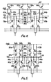
- Fig. 4 shows the connection of the decoder output unit, switching transistors and phototransistors of the second embodiment.
- reference numerals 77a, 77b, 78a and 78b designate load resistances connected to the output of decoder, 79a; 79b, 80a and 80b designate switching PNP transistors respectively, 81a, 81b, 82a and 82b designate load resistances for the switching PNP transistors 81a through 82b respectively, 83a, 83b, 84a and 84b designate switching NPN transistors for controlling charging currents to phototransistors 85a, 85b, 86a and 86b on or off according to whether or not terminal voltage exists on the load resistance 81a, 81b, 82a or 82b, and 87 designates a video output terminal in the common line for the emitters of phototransistors, the circuit of decoder unit being the same as the first embodiment.
- the switching PNP transistors are saturated, at the timing of turning said transistors off, the storage charges flow into the phototransistors, the recharge is developed, the auxiliary video signal appears on the video output line and mixes with the main video signal for the next phototransistor, thereby essentially lowering the resolution.
- the load resistances 81a, 81b, 82a and 82b are selected properly of each value, thereby enabling complete prevention of saturation of switching PNP transistors and improvement in the linearity of video output with respect to intensity of the light radiation.
- the switching NPN transistors act as buffers between the scanning signal line and the video output line, thereby improving a signal-to-noise ratio.
- FIG. 5 a third embodiment of the invention in accordance with Fig. 5, in which a decoder output unit, switching transistors and phototransistors, are connected with each other.
- reference numerals 88a, 88b, 89a and 89b designate load resistances connected to the outputs of the decoders
- 90a, 90b, 91a and 91b designate switching PNP transistors
- 92a, 92b, 93a and 93b designate load resistances for the switching PNP transistors respectively
- 94a, 94b, 95a and 95b designate switching NPN transistors for controlling charging currents to phototransistors 96a, 96b, 97a and 97b on or off according to whether or not terminal voltage exists on the load resistances 92a through 93b.
- the collectors of switching NPN transistors are connected to the emitters of phototransistors respectively, the collectors thereof being connected in common to form a video output terminal 98.
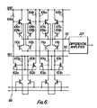
- reference numeral 99 designates a decoder unit the same as the first embodiment
- 100a, 100b, 101a and 101b designate load resistances connected to the outputs of decoders respectively
- 102a, 102b, 103a and 103b designate switching PNP transistors
- 104a, 104b, 105a and 105b designate load resistances for the switching PNP transistors 102a through 103a
- 106a, 106b, 107a and 107b designate switching NPN transistors for controlling on or off charging currents to phototransistors 108a, 110a, 108b, 110b, 109a, 111a, 109b and 111b, according to whether or not terminal voltages exist on the load resistance 104a, 104b, 105a, 105b, the phototransistors 108a, 108b, 109a and 109b constituting a first phototransistor array and
- the phototransistors 110a, 110b, 111a and 111b constitute a second phototransistor array and connect at the emitters to the collectors of corresponding switching NPN transistors 106a through 107b, and at the collectors in common, thereby forming a second video output terminal 113.
- the separate regions between the respective phototransistors similarly to the former embodiment, need not be interposed between the phototransistors connected at the collectors in common.
- One phototransistor array is provided with a light-receiving window and the other phototransistor array is light-shielded so that the video output signal is obtained from the common collector terminal at the phototransistors at the light receiving side and noise and dark signal output are obtained from the common collector terminal of phototransistors at the light shielding side, whereby a signal difference is picked up from both the terminals to enable cancellation of noise and dark signal caused by the noise current and the leakage current.
- the differential signal can be obtained by a differential amplifier 201.
- a driving circuit for the image sensor of the invention which comprises a timing controller 114, binary counters 115, a code converter 116, a shift register 117, and an image sensor 118.
- the driving circuit is given the start signal and clock signal from the system side, the timing controller 114 synchronizing start pulse (ST) with clock pulse, the counter 115 counting up the pulses up to the dot number of image sensor, and the code converter 116 converting a desired bit output (input bit of decoder) at the LSB side into the code in which the changed bit number of input signal is 1 during the scanning on the adjacent sensor, and thereafter applying the converted code into the decoder input terminals 119 within the image sensor.
- ST start pulse
- the counter 115 counting up the pulses up to the dot number of image sensor
- the code converter 116 converting a desired bit output (input bit of decoder) at the LSB side into the code in which the changed bit number of input signal is 1 during the scanning on the adjacent sensor, and thereafter applying the converted code
- Block selecting input signals 120 are given from the output of shift register 117 shifting at the timing of carry of decoder input signal.
- the scanning in the reverse direction may be applicable in such a manner that the counters may be put in a down count mode and the shift register may shift at the timing of borrow of decoder input signal, thus making it possible to read the original in the reverse direction.
Landscapes
- Engineering & Computer Science (AREA)
- Multimedia (AREA)
- Signal Processing (AREA)
- Facsimile Heads (AREA)
- Transforming Light Signals Into Electric Signals (AREA)
Claims (20)
- Ein selbstabtastender Bildsensor zum Umwandeln eines optischen Signales in ein elektrisches Signal, mit: einem Phototransistorfeld (68), das aus einer Vielzahl von Phototransistoren zum Umwandeln eines optischen Signales in ein elektrisches Stromsignal zusammengesetzt ist;
einem ersten Stromschalterfeld (67), das aus einer Vielzahl von Stromschaltern, welche jeweils mit der Vielzahl von Phototransistoren verbunden sind, zusammengesetzt ist;
einer Vielzahl von Decoderschaltkreisen (59 - 62), jeweils für die Auswahl von einem aus der Vielzahl von Stromschaltern des ersten Stromschalterfeldes entsprechend einem ersten Steuersignal, das gemeinsam an die Vielzahl von Decoderschaltkreisen angelegt wird, wobei die Ausgänge der Vielzahl von Decoderschaltkreisen mit den Stromschaltern des ersten Stromschalterfeldes korrespondieren;
einem zweiten Stromschalterfeld (63), das aus einer Vielzahl von Stromschaltern für die Auswahl von einem aus der Vielzahl von Decoderschaltkreisen entsprechend einem zweiten Steuersignal zusammengesetzt ist;
einem Stromquellenschaltkreis (65) für die Lieferung eines Stromes zu dem ausgewählten einen aus der Vielzahl von Decoderschaltkreisen über den ausgewählten einen aus der Vielzahl von Stromschaltern des zweiten Stromschalterfeldes;
einem Treibschaltkreis (70) für die Erzeugung des ersten Steuersignales, das an jeden aus der Vielzahl von Decoderschaltkreisen angelegt wird, und des zweiten Steuersignales, das an das zweite Stromschalterfeld angelegt wird; und mit
einem Ausgabeschaltkreis (200) für die Umwandlung des Stromsignales aus dem Phototransistorfeld in ein Spannungssignal. - Der Bildsensor nach Anspruch 1,
wobei jeder aus der Vielzahl von Decoderschaltkreisen eine Vielzahl von Abschnitten von Stromschalterfeldern, die aus einer Vielzahl von Stromumstellungsschaltern (19 - 25) zusammengesetzt sind, wovon jeder einen gemeinsamen Eingangsanschluß, zwei Ausgangsanschlüsse und zwei Steueranschlüsse entsprechend den zwei Ausgangsanschlüssen aufweist, umfaßt; wobei der erste Abschnitt der Vielzahl von Abschnitten der Stromschalter einen einzelnen Stromumstellungsschalter (19) umfaßt, der an seinem gemeinsamen Eingangsanschluß mit einem (17) von der Vielzahl von Stromschaltern des zweiten Stromschalterfeldes verbunden ist; die zwei Ausgangsanschlüsse von jedem der Vielzahl von Stromumstellungsschaltern von den letzten Abschnitten (22 - 25) der Vielzahl von Abschnitten von Stromschalterfeldern jeweils mit zweien aus der Vielzahl von Stromschaltern (30a, 30b - 33a, 33b) des ersten Stromschalterfeldes verbunden sind; jeder aus der Vielzahl von Stromumstellungsschaltern der anderen Abschnitte (20, 21) der Vielzahl von Abschnitten von Stromschalterfeldern an seinem gemeinsamen Eingangsanschluß mit einem Ausgangsanschluß von einem aus der Vielzahl von Stromumstellungsschaltern des vorhergehenden Abschnittes und an seinen zwei Ausgangsanschlüssen mit den gemeinsamen Eingangsanschlüssen von zweien aus der Vielzahl von Stromumstellungsschaltern des nächsten Abschnittes verbunden ist, um dadurch baumförmig verbunden zu sein, und wobei das erste Steuersignal aus einer Vielzahl von Paaren von komplementären Signalen (A,A , B,B , C,C ) zusammengesetzt ist, die jeweils an die Vielzahl von Abschnitten der Stromschalterfelder angelegt werden, wobei jedes Paar der Vielzahl der Paare von komplementären Signalen jeweils an die zwei Steueranschlüsse der Vielzahl der Stromumstellungsschalter von jedem aus der Vielzahl der Abschnitte der Stromschalterfelder angelegt wird. - Die Vorrichtung nach Anspruch 2,
wobei jeder aus der Vielzahl von Umstellungsschaltern (19 - 25) ein Paar von Transistoren umfaßt, welche an den Emittern zur Bildung des gemeinsamen Eingangsanschlusses verbunden sind, wobei die Kollektoren des Paares von Transistoren die zwei Ausgangsanschlüsse und die Basisanschlüsse des Paares von Transistoren die zwei Steueranschlüsse sind. - Der Bildsensor nach Anspruch 2,
wobei der Treibschaltkreis (70) einen Zählerschaltkreis (115), der mit einem Taktsignal als Eingangssignal beaufschlagt wird, einen Codeänderungsschaltkreis (116) zum Umwandeln eines parallelen Ausgangssignales des Zählers in ein spezifiziertes codiertes Signal, einen ersten Steuersignalerzeugungsschaltkreis (72) zur Erzeugung des ersten Steuersignales aus dem spezifizierten codierten Signal, und einen zweiten Steuersignalerzeugungsschaltkreis (75), der mit dem am meisten signifikanten Bit-Signal des parallelen Ausgangssignales des Zählers als Eingangssignal zur Erzeugung des zweiten Steuersignales beaufschlagt wird. - Der Bildsensor nach Anpruch 4,
wobei der erste Steuersignalerzeugungsschaltkreis (72) eine Vielzahl von Exklusiv-Oder-Gattern umfaßt, die parallelen Ausgangsanschlüssen des Zählers entsprechen, wobei jedes aus der Vielzahl von Exklusiv-Oder-Gattern an einem Eingangsanschluß mit einem entsprechenden Ein-Bit-Anschluß der parallelen Ausgangsanschlüsse des Zählers und an dem anderen Eingangsanschluß mit dem nächsthöheren Bit-Anschluß der parallelen Ausgangsanschlüsse des Zählers verbunden ist, und der andere Eingangsanschluß von einem aus der Vielzahl von Exklusiv-Oder-Gattern, der dem am meisten signifikanten Bit-Anschluß entspricht, mit dem Übertraganschluß des Zählers verbunden ist, um dadurch das spezifizierte codierte Signal an den Ausgangsanschlüssen der Vielzahl von Exklusiv-Oder-Gattern zu erzeugen; und wobei der zweite Steuersignalerzeugungsschaltkreis (75) ein Schieberegister umfaßt, um das zweite Steuersignal an seinen parallelen Ausgangsanschlüssen zu bilden, wodurch die Vielzahl von Phototransistoren in einer sequentiellen Reihenfolge aktiviert wird. - Der Bildsensor nach Anspruch 1,
wobei jeder von der Vielzahl von Stromschaltern (30a, 30b - 33a, 33b) des ersten Stromschalterfeldes (67) einen PNP-Transistor umfaßt, der an der Basis mit einem der Ausgangsanschlüsse der Vielzahl von Decoderschaltkreisen (59 - 62), an dem Kollektor mit einer positiven Spannungsquelle (Vcc), und am Emitter mit dem Kollektor von einem aus der Vielzahl von Phototransistoren (34a - 37b) verbunden ist, wobei die Emitter von der Vielzahl von Phototransistoren zusammengeschlossen sind, um einen Ausgangsanschluß des Phototransistorfeldes zu bilden. - Der Bildsensor nach Anspruch 1,
wobei jeder aus der Vielzahl von Schaltern (30a - 33b) des ersten Stromschalterfeldes (67) einen komplementären PNP-Transistor umfaßt, der aus einem PNP-Transistor und einem NPN-Transistor, welche in einer komplementären Darlingtonschaltung verbunden sind, zusammengesetzt ist, wobei der PNP-Transistor an der Basis mit einem von den Ausgangsanschlüssen von der Vielzahl von Decoderschaltkreisen verbunden ist, am Emitter mit einer positiven Spannungsquelle, und am Kollektor mit der Basis des NPN-Transistors über einen Widerstand verbunden ist; und wobei der NPN-Transistor an dem Kollektor mit der positiven Spannungsquelle, und am Emitter mit einem Kollektor von einem von der Vielzahl von Phototransistoren verbunden ist, wobei die Emitter der Vielzahl von Phototransistoren gemeinsam zusammengeschlossen sind, um einen Ausgangsanschluß (38) des Phototransistorfeldes zu bilden. - Ein selbstabtastender Bildsensor zum Umwandeln eines optischen Signales in ein elektrisches Signal, mit:
einem Phototransistorfeld, das aus einer Vielzahl von Phototransistoren (85a, 85b) zum Umwandeln eines optischen Signales in ein elektrisches Stromsignal zusammengesetzt ist;
einem NPN-Transistorfeld, das aus einer Vielzahl von NPN-Transistoren (83a, 84b) welche jeweils mit der Vielzahl von Phototransistoren verbunden sind, zusammengesetzt ist;
einem PNP-Transistorfeld, das aus einer Vielzahl von PNP-Transistoren (79a - 80b), welche jeweils mit der Vielzahl von NPN-Transistoren verbunden sind, zusammengesetzt ist;
einer Vielzahl von Decoderschaltkreisen (59 - 62), jeweils für die Auswahl von einem aus der Vielzahl von PNP-Transistoren entsprechend einem ersten Steuersignal, das gemeinsem an die Vielzahl von PNP-Transistoren gelegt wird, wobei die Ausgänge der Vielzahl von Decoderschaltkreisen mit der Vielzahl von PNP-Transistoren korrespondieren;
einem Stromschalterfeld (63), das aus einer Vielzahl von Stromschaltern für die Auswahl von einem von der Vielzahl von Decoderschaltkreisen entsprechend einem zweiten Steuersignal zusammengesetzt ist;
einem Stromquellenschaltkreis (65) für die Lieferung eines Stromes zu dem ausgewählten einen von der Vielzahl von Decoderschaltkreisen über einen ausgewählten einen aus der Vielzahl von Stromschaltern des Stromschalterfeldes;
einem Treibschaltkreis (70) zum Erzeugen des ersten Steuersignales, das an jeden von der Vielzahl von Decoderschaltkreisen gelegt wird, und des zweiten Steuersignales, das an das Stromschalterfeld gelegt wird; und
einem Ausgabeschaltkreis (200) für die Umwandlung des Stromsignales aus dem Phototransistorfeld in ein Spannungssignal. - Der Bildsensor nach Anspruch 8,
wobei jeder von der Vielzahl von Decoderschaltkreisen eine Vielzahl von Abschnitten von Stromschalterfeldern (19 - 25) umfaßt, welche aus einer Vielzahl von Stromumstellungsschaltern zusammengesetzt sind, von denen jeder einen gemeinsamen Eingangsanschluß, zwei Ausgangsanschlüsse und zwei Steueranschlüsse entsprechend den zwei Ausgangsanschlüssen aufweist; wobei der erste Abschnitt von der Vielzahl der Abschnitte von Stromschalterfeldern einen einzelnen Stomumstellungsschalter (19) umfaßt, der an seinem gemeinsamen Eingangsanschluß mit einem (17) aus der Vielzahl von Stromschaltern des Stromschalterfeldes verbunden ist; die zwei Ausgangsanschlüsse von jedem aus der Vielzahl von Stromumstellungsschaltern der letzten Abschnitte (22 - 25) der Vielzahl der Abschnitte von Stromschalterfeldern jeweils mit zwei Transistoren von der Vielzahl von PNP-Transistoren des PNP-Transistorfeldes (79a - 80b) verbunden ist; jeder von der Vielzahl von Stromumstellungsschaltern des anderen Abschnittes (20, 21) der Vielzahl der Abschnitte von Stromschalterfeldern mit seinem gemeinsamen Eingangsanschluß mit einem Ausgangsanschluß von einem aus der Vielzahl der Stromumstellungsschalter des vorhergehenden Abschnittes und an seinen zwei Ausgangsanschlüssen mit den gemeinsamen Eingangsanschlüssen von zwei Schaltern aus der Vielzahl von Stromumstellungsschaltern des nächsten Abschnittes verbunden ist, um so baumartig verbunden zu sein, und wobei das erste Steuersignal aus einer Vielzahl von Paaren von komplementären Signalen (A,A , B,B , C,C ) zusammengesetzt ist, die jeweils an die Vielzahl von Abschnitten der Stromschalterfelder gelegt werden, wobei jedes Paar aus der Vielzahl der Paare von komplementären Signalen jeweils an die zwei Steuereingänge der Vielzahl von Stromumstellungsschaltern von jedem der Vielzahl der Abschnitte von Stromschalterfeldern gelegt wird. - Die Vorrichtung nach Anspruch 9,
wobei jeder aus der Vielzahl von Umstellungsschaltern (19025) ein Paar von Transistoren umfaßt, welche an den Emittern als der gemeinsame Eingangsanschluß zusammengeschaltet sind, wobei die Kollektoren des Paares von Transistoren die zwei Ausgangsanschlüsse und die Basisanschlüsse des Paares von Transistoren die zwei Steueranschlüsse bilden. - Der Bildsensor nach Anspruch 9,
wobei der Treibschaltkreis (70) einen Zählerschaltkreis (115), der mit einem Taktsignal als Eingangssignal beaufschlagt wird, einen Codeänderungsschaltkreis (116) zum Umwandeln eines parallelen Ausgangssignales des Zählers in ein spezifiziertes codiertes Signal, einen ersten Steuersignalerzeugungsschaltkreis (72) zum Erzeugen des ersten Steuersignales aus dem spezifizierten codierten Signal, und einen zweiten Steuersignalerzeugungsschaltkreis (75), der mit dem am meisten signifikanten Bit-Signal des parallelen Ausgangssignales des Zählers als Eingangssignal zum Erzeugen des zweiten Steuersignales beaufschlagt wird. - Der Bildsensor nach Anspruch 11,
wobei der erste Steuersignalerzeugungsschaltkreis (72) eine Vielzahl von Exklusiv-Oder-Gattern umfaßt, die den parallelen Ausgangsanschlüssen des Zählers entsprechen, wobei jedes der Vielzahl von Exklusiv-Oder-Gattern an einem Eingangsanschluß mit einem entsprechenden Bit-Anschluß der parallelen Ausgangsanschlüsse des Zählers und an dem anderen Eingangsanschluß mit dem nächsthöheren Bit-Anschluß der parallelen Ausgangsanschlüsse des Zählers verbunden ist, wobei der andere Eingangsanschluß von einem der Vielzahl von Exklusiv-Oder-Gattern, der dem am meisten signifikanten Bit-Anschluß entspricht, mit dem Übertraganschluß des Zählers verbunden ist, um dadurch das spezifizierte codierte Signal an den Ausgangsanschlüssen der Vielzahl von Exklusiv-Oder-Gattern zu erzeugen; und wobei der zweite Steuersignalerzeugungsschaltkreis (75) ein Schieberegister umfaßt, um das zweite Steuersignal an seinen parallelen Ausgangsanschlüssen zu erzeugen, wodurch die Vielzahl von Phototransistoren in einer sequenziellen Reihenfolge aktiviert wird. - Der Bildsensor nach Anspruch 8,
wobei die Vielzahl von PNP-Transistoren (79a - 80b) an den Kollektoren jeweils mit den Basisanschlüssen der Vielzahl von NPN-Transistoren (83a - 84b), an den Basisanschlüssen jeweils mit den Ausgangsanschlüssen der Vielzahl von Decoderschaltkreisen (59 - 62) und jeweils einer positiven Spannungsquelle über einen Widerstand verbunden und an den Emittern zusammengeführt ist; und wobei die Vielzahl von NPN-Transistoren (83a - 84b) an den Emittern mit einer positiven Spannungsquelle (Vcc) und an den Kollektoren jeweils mit den Basisanschlüssen der Vielzahl von Phototransistoren (85a - 86b) verbunden ist, wobei die Kollektoren der Vielzahl von Phototransistoren zusammengeschaltet sind, um einen Ausgangsanschluß (87) des Phototransistorfeldes zu bilden. - Der Bildsensor nach Anspruch 13,
welcher ferner ein zweites Phototransistorfeld umfaßt, welches aus einer Vielzahl von Phototransistoren (110a - 111b) zusammengesetzt ist, welche an den Kollektoren zusammengeschaltet sind, um einen Ausgangsanschluß (113) des zweiten Phototransistorfeldes zu bilden, wobei die Vielzahl von NPN-Transistoren (106a - 107b) Doppelkollektor-NPN-Transistoren umfaßt, welche jeweils zwei Kollektoren aufweisen, wobei die zweiten Kollektoren der Doppelkollektor-NPN-Transistoren mit den Emittern der Vielzahl von Phototransistoren des zweiten Phototransistorfeldes verbunden sind. - Der Bildsensor nach Anspruch 14,
welcher ferner ein Lichtempfangsfenster, das auf dem Phototransistorfeld vorgesehen ist, und eine Lichtunterbrechungsabdeckung, die auf dem zweiten Phototransistorfeld vorgesehen ist, umfaßt; und wobei der Ausgabeschaltkreis einen Differentialverstärker (201) umfaßt, welcher an seinen Differenzeingangsanschlüssen mit dem jeweiligen Ausgangsanschluß des Phototransistorfeldes bzw. des zweiten Phototransistorfeldes verbunden ist, um dadurch ein Störsignal und Dunkelstromsignal, das in dem Stromsignal aus dem Phototransistorfeld enthalten ist, aufzuheben. - Ein selbstabtastender Bildsensor zum Umwandeln eines optischen Signales in ein elektrisches Signal, mit:
einem Phototransistorfeld, das aus einer Vielzahl von Phototransistoren (96a - 97b) zusammengesetzt ist, welche an den Kollektoren zusammengeschaltet sind, zum Umwandeln eines optischen Signales in ein elektrisches Stromsignal;
einem NPN-Transistorfeld, das aus einer Vielzahl von NPN-Transistoren (94a - 95b) zusammengesetzt ist, welche an den Kollektoren jeweils mit den Emittern der Vielzahl von Phototransistoren und an den Emittern mit einer positiven Spannungsquelle verbunden sind;
einem PNP-Transistorfeld, das aus einer Vielzahl von PNP-Transistoren (90a - 91b) zusammengesetzt ist, welche an den Kollektoren jeweils mit den Basisanschlüssen der Vielzahl von NPN-Transistoren und an den Basisanschlüssen jeweils mit der positiven Spannungsquelle über Widerstände verbunden sind;
einer Vielzahl von Decoderschaltkreisen (59 - 62) jeweils für die Auswahl von einem aus der Vielzahl von PNP-Transistoren entsprechend einem ersten Steuersignal, das gemeinsam an die Vielzahl von PNP-Transistoren gelegt wird, wobei die Ausgänge der Vielzahl von Decoderschaltkreisen mit der Vielzahl von PNP-Transistoren korrespondieren;
einem Stromschalterfeld (63), das aus einer Vielzahl von Stromschaltern zum Auswählen von einem aus der Vielzahl von Decoderschaltkreisen entsprechend einem zweiten Steuersignal zusammengesetzt ist;
einem Stromquellenschaltkreis (65) für die Lieferung eines Stromes zu dem ausgewählten einen aus der Vielzahl von Decoderschaltkreisen über einen ausgewählten einen aus der Vielzahl von Stromschaltern des Stromschalterfeldes;
einem Treibschaltkreis (70) zum Erzeugen des ersten Steuersignales, das an jeden von der Vielzahl von Decoderschaltkreisen gelegt wird, und des zweiten Steuersignales, das an das Stromschalterfeld gelegt wird; und
einem Ausgabeschaltkreis (200) zum Umwandeln des Stromsignales aus dem Phototransistorfeld in ein Spannungssignal; wobei jeder von der Vielzahl von Decoderschaltkreisen eine Vielzahl von Abschnitten von Transistorfeldern umfaßt, welche aus einer Vielzahl von Paaren von Transistoren (19 - 25) zusammengesetzt sind, wobei jedes Paar an den Emittern zusammengeschaltet ist, der erste Abschnitt der Vielzahl von Abschnitten von Transistorfeldern ein einzelnes Paar von Transistoren (19) umfaßt, welche an dem gemeinsamen Emitter mit einem von der Vielzahl von Stromschaltern des Stromschalterfeldes verbunden sind, wobei die Kollektoren der Vielzahl von Paaren von Transistoren der letzten Abschnitte (22 - 25) der Vielzahl der Abschnitte von Transistorfeldern jeweils mit den Basisanschlüssen der Vielzahl von PNP-Transistoren des PNP-Transistorfeldes verbunden sind, jedes der Vielzahl von Paaren von Transistoren der anderen Abschnitte (20, 21) der Vielzahl von Abschnitten von Transistorfeldern an den gemeinsamen Emittern mit einem Kollektor von einem von der Vielzahl von Paaren von Transistoren des vorherigen Abschnittes und an den zwei Kollektoren mit den gemeinsamen Emittern von zweien aus der Vielzahl von Paaren von Transistoren des nächsten Abschnittes verbunden ist, um dadurch baumartig verbunden zu sein, und wobei das erste Steuersignal aus einer Vielzahl von Paaren komplementärer Signale (A,A , B,B , C,C ) zusammengesetzt ist, die jeweils an die Vielzahl der Abschnitte von Stromschalterfeldern gelegt werden, wobei jedes Paar der Vielzahl der Paare komplementärer Signale jeweils an die Basisanschlüsse der Vielzahl der Paare von Transistoren von jedem der Vielzahl der Abschnitte von Transistorfeldern gelegt wird. - Der Bildsensor nach Anspruch 16,
wobei der Treibschaltkreis (70) einen Zählerschaltkreis (115), der mit einem Taktsignal als Eingangssignal beaufschlagt wird, einen Codeänderungsschaltkreis (116) zum Umwandeln eines parallelen Ausgangssignales des Zählers in ein spezifiziertes codiertes Signal, einen ersten Steuersignalerzeugungsschaltkreis (72) zum Erzeugen des ersten Steuersignales aus dem spezifizieren codierten Signal, und einen zweiten Steuersignalerzeugungsschaltkreis (75) umfaßt, der mit dem am meisten signifikanten Bit-Signal des parallelen Ausgangssignales des Zählers als Eingangssignal zur Erzeugung des zweiten Steuersignales beaufschlagt wird. - Der Bildsensor nach Anspruch 17,
wobei der erste Steuersignalerzeugungsschaltkreis (72) eine Vielzahl von Exklusiv-Oder-Gattern entsprechend den parallelen Ausgangsanschlüssen des Zählers umfaßt, wobei jedes aus der Vielzahl von Exklusiv-Oder-Gattern an einem Eingangsanschluß mit einem entsprechenden Ein-Bit-Anschluß der parallelen Ausgangsanschlüsse des Zählers und an dem anderen Eingangsanschluß mit dem nächsthöheren Bit-Anschluß der parallelen Ausgangsanschlüsse des Zählers verbunden ist, und der andere Eingangsanschluß von einem aus der Vielzahl von Exklusiv-Oder-Gattern, der dem am meisten signifikanten Bit-Anschluß entspricht, mit dem Übertraganschluß des Zählers verbunden ist, um dadurch das spezifizierte codierte Signal an Ausgangsanschlüssen der Vielzahl von Exclusiv-Oder-Gattern zu erzeugen; und wobei der das zweite Steuersignal erzeugende Schaltkreis ein Schieberegister umfaßt, um das zweite Steuersignal an seinen parallelen Ausgangsanschlüssen zu erzeugen, wodurch die Vielzahl von Phototransistoren in einer sequentiellen Reihenfolge aktiviert wird. - Der Bildsensor nach Anspruch 16,
welcher ferner ein zweites Phototransistorfeld umfaßt, das aus einer Vielzahl von Phototransistoren (110a - 111b) zusammengesetzt ist, welche an den Kollektoren zusammengeschaltet sind, wobei die Vielzahl von NPN-Transistoren (106a - 107b) Doppelkollektor-NPN-Transistoren sind, welche zweite Kollektoren aufweisen, die mit den Emittern der Vielzahl von Phototransistoren des zweiten Phototransistorfeldes verbunden sind. - Der Bildsensor nach Anspruch 19,
welcher ferner ein Lichtempfangsfenster, das auf dem Phototransistorfeld vorgesehen ist, und eine Lichtabschirmungsabdeckung, die auf dem zweiten Phototransistorfeld vorgesehen ist, umfaßt; und wobei der Ausgabeschaltkreis einen Differenzverstärker (201) umfaßt, welcher an seinen Differenzeingangsanschlüssen jeweils mit den gemeinsamen Kollektoren des Phototransistorfeldes und des zweiten Phototransistorfeldes verbunden ist, um so ein Störsignal und ein Dunkelstromsignal, das in dem Stromsignal aus dem Phototransistorfeld enthalten ist, auszuschalten.
Applications Claiming Priority (4)
| Application Number | Priority Date | Filing Date | Title |
|---|---|---|---|
| JP200294/83 | 1983-10-26 | ||
| JP58200294A JPS6091758A (ja) | 1983-10-26 | 1983-10-26 | イメ−ジセンサ |
| JP59000976A JPS60144070A (ja) | 1984-01-06 | 1984-01-06 | カラ−イメ−ジセンサ |
| JP976/84 | 1984-01-06 |
Publications (3)
| Publication Number | Publication Date |
|---|---|
| EP0141486A2 EP0141486A2 (de) | 1985-05-15 |
| EP0141486A3 EP0141486A3 (en) | 1988-07-20 |
| EP0141486B1 true EP0141486B1 (de) | 1991-09-11 |
Family
ID=26334101
Family Applications (1)
| Application Number | Title | Priority Date | Filing Date |
|---|---|---|---|
| EP84303897A Expired - Lifetime EP0141486B1 (de) | 1983-10-26 | 1984-06-08 | Bildsensor |
Country Status (3)
| Country | Link |
|---|---|
| US (1) | US4567529A (de) |
| EP (1) | EP0141486B1 (de) |
| DE (1) | DE3485050D1 (de) |
Families Citing this family (22)
| Publication number | Priority date | Publication date | Assignee | Title |
|---|---|---|---|---|
| CA1263175A (en) * | 1984-05-28 | 1989-11-21 | Hideyuki Miyazawa | Image reader for image processing apparatus |
| JPS6154756A (ja) * | 1984-08-25 | 1986-03-19 | Fuji Electric Corp Res & Dev Ltd | 密着型イメ−ジセンサ |
| US4763189A (en) * | 1984-08-31 | 1988-08-09 | Canon Kabushiki Kaisha | Color image sensor with three line sensors on different layers separated by electrically-insulating layers |
| DE3604971A1 (de) * | 1986-02-17 | 1987-08-20 | Messerschmitt Boelkow Blohm | Photosensoreinrichtung mit dunkelstromkompensation |
| EP0234909A3 (de) * | 1986-02-26 | 1990-01-24 | Matsushita Electric Industrial Co., Ltd. | Bildsensor |
| JPS62293384A (ja) * | 1986-06-11 | 1987-12-19 | Toshiba Corp | 画像入力装置 |
| DE3804200A1 (de) * | 1988-02-11 | 1989-08-24 | Messerschmitt Boelkow Blohm | Photoelektrischer liniensensor |
| JP3120237B2 (ja) * | 1990-01-10 | 2000-12-25 | セイコーインスツルメンツ株式会社 | イメージセンサ |
| EP0456193B1 (de) * | 1990-05-09 | 1999-01-20 | Matsushita Electric Industrial Co., Ltd. | Bildaufnahmegerät mit darin verwendeter Zählerschaltung |
| US5128778A (en) * | 1990-09-28 | 1992-07-07 | Xerox Corporation | Fast scan imaging area optimization system |
| US6786420B1 (en) | 1997-07-15 | 2004-09-07 | Silverbrook Research Pty. Ltd. | Data distribution mechanism in the form of ink dots on cards |
| US6618117B2 (en) | 1997-07-12 | 2003-09-09 | Silverbrook Research Pty Ltd | Image sensing apparatus including a microcontroller |
| US6690419B1 (en) * | 1997-07-15 | 2004-02-10 | Silverbrook Research Pty Ltd | Utilising eye detection methods for image processing in a digital image camera |
| US6624848B1 (en) * | 1997-07-15 | 2003-09-23 | Silverbrook Research Pty Ltd | Cascading image modification using multiple digital cameras incorporating image processing |
| US6879341B1 (en) | 1997-07-15 | 2005-04-12 | Silverbrook Research Pty Ltd | Digital camera system containing a VLIW vector processor |
| US20040119829A1 (en) * | 1997-07-15 | 2004-06-24 | Silverbrook Research Pty Ltd | Printhead assembly for a print on demand digital camera system |
| US7110024B1 (en) | 1997-07-15 | 2006-09-19 | Silverbrook Research Pty Ltd | Digital camera system having motion deblurring means |
| US6014160A (en) * | 1998-03-30 | 2000-01-11 | Xerox Corporation | Image scanning array having independently addressable photosensor chips |
| AUPP702098A0 (en) | 1998-11-09 | 1998-12-03 | Silverbrook Research Pty Ltd | Image creation method and apparatus (ART73) |
| AUPQ056099A0 (en) * | 1999-05-25 | 1999-06-17 | Silverbrook Research Pty Ltd | A method and apparatus (pprint01) |
| US6796955B2 (en) * | 2002-02-14 | 2004-09-28 | Chf Solutions, Inc. | Method to control blood and filtrate flowing through an extracorporeal device |
| US7164506B2 (en) * | 2002-06-07 | 2007-01-16 | Xerox Corporation | Multi-chip image sensor, on chip apparatus for causing each chip to selectably function in a parallel or serial readout |
Family Cites Families (8)
| Publication number | Priority date | Publication date | Assignee | Title |
|---|---|---|---|---|
| FR2356328A1 (fr) * | 1976-06-24 | 1978-01-20 | Ibm France | Dispositif d'elimination du bruit dans les reseaux photosensibles a auto-balayage |
| US4141018A (en) * | 1976-11-08 | 1979-02-20 | Tokyo Shibaura Electric Co., Ltd. | Thermal recording head and drive circuit |
| JPS5419320A (en) * | 1977-07-14 | 1979-02-14 | Ricoh Co Ltd | Copying machine of electrostatic recording type |
| JPS5518151A (en) * | 1978-07-26 | 1980-02-08 | Canon Inc | Input device of photo electric conversion information |
| US4237383A (en) * | 1978-09-20 | 1980-12-02 | Rca Corporation | High speed loading of output register of CCD array system |
| US4405857A (en) * | 1980-03-31 | 1983-09-20 | Canon Kabushiki Kaisha | Solid-state photoelectric converter |
| GB2103049B (en) * | 1981-06-25 | 1985-02-20 | Nippon Telegraph & Telephone | Image sensor |
| US4495409A (en) * | 1982-02-16 | 1985-01-22 | Hitachi, Ltd. | Photosensor with diode array |
-
1984
- 1984-06-05 US US06/617,566 patent/US4567529A/en not_active Expired - Fee Related
- 1984-06-08 EP EP84303897A patent/EP0141486B1/de not_active Expired - Lifetime
- 1984-06-08 DE DE8484303897T patent/DE3485050D1/de not_active Expired - Lifetime
Also Published As
| Publication number | Publication date |
|---|---|
| EP0141486A2 (de) | 1985-05-15 |
| EP0141486A3 (en) | 1988-07-20 |
| DE3485050D1 (de) | 1991-10-17 |
| US4567529A (en) | 1986-01-28 |
Similar Documents
| Publication | Publication Date | Title |
|---|---|---|
| US4567529A (en) | Image sensor | |
| US5650864A (en) | Full color single-sensor-array contact image sensor (CIS) using advanced signal processing techniques | |
| EP0493455B1 (de) | I.c. sensor | |
| EP0272152B1 (de) | Signalausleseschaltung | |
| US7626620B2 (en) | Photoelectric conversion unit stacked structure | |
| US5726439A (en) | Image sensor comprising a two-dimensional array of photodetectors with both column and row output circuits which are in parallel | |
| US5933188A (en) | Photoelectric conversion apparatus and method with reset | |
| JP2000032350A (ja) | 画素毎のa/d変換器を備えるcmos撮像装置 | |
| JPH11205695A (ja) | 遅延移送周波数変調付きイメージセンシングデバイス | |
| US4413283A (en) | Solid-state imaging device | |
| US4634886A (en) | Photoelectric imager with a high S/N ratio | |
| US5027226A (en) | Contact type image sensor | |
| US5262850A (en) | Photoelectric converting device having reduced line sensor space | |
| US6657664B2 (en) | Solid-state image pickup device | |
| US5724094A (en) | Contact image sensor utilizing differential voltage pickoff | |
| US20020135827A1 (en) | Image processing apparatus | |
| JPH09205518A (ja) | イメージセンサおよびイメージセンサチップ | |
| US7015449B2 (en) | Linear image sensor | |
| US6943721B1 (en) | Charge-coupled amplifier and converter with matched offsets | |
| CN1725504B (zh) | 光电转换器及图像传感器 | |
| US20050094222A1 (en) | High resolution, high sensitivity image scanner having noise cancellation improvements | |
| US7218350B2 (en) | Image sensor with digital output and inherent pixel non-uniformity suppression | |
| JPH063960B2 (ja) | バイポ−ラicイメ−ジセンサ | |
| JPH0215147B2 (de) | ||
| US4845567A (en) | Image sensor |
Legal Events
| Date | Code | Title | Description |
|---|---|---|---|
| PUAI | Public reference made under article 153(3) epc to a published international application that has entered the european phase |
Free format text: ORIGINAL CODE: 0009012 |
|
| AK | Designated contracting states |
Designated state(s): DE FR GB NL |
|
| PUAL | Search report despatched |
Free format text: ORIGINAL CODE: 0009013 |
|
| AK | Designated contracting states |
Kind code of ref document: A3 Designated state(s): DE FR GB NL |
|
| 17P | Request for examination filed |
Effective date: 19890113 |
|
| 17Q | First examination report despatched |
Effective date: 19900510 |
|
| GRAA | (expected) grant |
Free format text: ORIGINAL CODE: 0009210 |
|
| AK | Designated contracting states |
Kind code of ref document: B1 Designated state(s): DE FR GB NL |
|
| PG25 | Lapsed in a contracting state [announced via postgrant information from national office to epo] |
Ref country code: NL Effective date: 19910911 |
|
| REF | Corresponds to: |
Ref document number: 3485050 Country of ref document: DE Date of ref document: 19911017 |
|
| ET | Fr: translation filed | ||
| NLV1 | Nl: lapsed or annulled due to failure to fulfill the requirements of art. 29p and 29m of the patents act | ||
| PLBE | No opposition filed within time limit |
Free format text: ORIGINAL CODE: 0009261 |
|
| STAA | Information on the status of an ep patent application or granted ep patent |
Free format text: STATUS: NO OPPOSITION FILED WITHIN TIME LIMIT |
|
| 26N | No opposition filed | ||
| PGFP | Annual fee paid to national office [announced via postgrant information from national office to epo] |
Ref country code: GB Payment date: 19940601 Year of fee payment: 11 |
|
| PGFP | Annual fee paid to national office [announced via postgrant information from national office to epo] |
Ref country code: DE Payment date: 19940608 Year of fee payment: 11 |
|
| PGFP | Annual fee paid to national office [announced via postgrant information from national office to epo] |
Ref country code: FR Payment date: 19940609 Year of fee payment: 11 |
|
| PG25 | Lapsed in a contracting state [announced via postgrant information from national office to epo] |
Ref country code: GB Effective date: 19950608 |
|
| GBPC | Gb: european patent ceased through non-payment of renewal fee |
Effective date: 19950608 |
|
| PG25 | Lapsed in a contracting state [announced via postgrant information from national office to epo] |
Ref country code: FR Effective date: 19960229 |
|
| PG25 | Lapsed in a contracting state [announced via postgrant information from national office to epo] |
Ref country code: DE Effective date: 19960301 |
|
| REG | Reference to a national code |
Ref country code: FR Ref legal event code: ST |