EP0141538A1 - Thyristor à induction statique - Google Patents
Thyristor à induction statique Download PDFInfo
- Publication number
- EP0141538A1 EP0141538A1 EP84306785A EP84306785A EP0141538A1 EP 0141538 A1 EP0141538 A1 EP 0141538A1 EP 84306785 A EP84306785 A EP 84306785A EP 84306785 A EP84306785 A EP 84306785A EP 0141538 A1 EP0141538 A1 EP 0141538A1
- Authority
- EP
- European Patent Office
- Prior art keywords
- layer
- high concentration
- semiconductor layer
- buried gate
- gate
- Prior art date
- Legal status (The legal status is an assumption and is not a legal conclusion. Google has not performed a legal analysis and makes no representation as to the accuracy of the status listed.)
- Granted
Links
Images




Classifications
-
- H—ELECTRICITY
- H10—SEMICONDUCTOR DEVICES; ELECTRIC SOLID-STATE DEVICES NOT OTHERWISE PROVIDED FOR
- H10D—INORGANIC ELECTRIC SEMICONDUCTOR DEVICES
- H10D62/00—Semiconductor bodies, or regions thereof, of devices having potential barriers
- H10D62/10—Shapes, relative sizes or dispositions of the regions of the semiconductor bodies; Shapes of the semiconductor bodies
- H10D62/13—Semiconductor regions connected to electrodes carrying current to be rectified, amplified or switched, e.g. source or drain regions
- H10D62/149—Source or drain regions of field-effect devices
-
- H—ELECTRICITY
- H10—SEMICONDUCTOR DEVICES; ELECTRIC SOLID-STATE DEVICES NOT OTHERWISE PROVIDED FOR
- H10D—INORGANIC ELECTRIC SEMICONDUCTOR DEVICES
- H10D12/00—Bipolar devices controlled by the field effect, e.g. insulated-gate bipolar transistors [IGBT]
- H10D12/211—Gated diodes
- H10D12/212—Gated diodes having PN junction gates, e.g. field controlled diodes
-
- H—ELECTRICITY
- H10—SEMICONDUCTOR DEVICES; ELECTRIC SOLID-STATE DEVICES NOT OTHERWISE PROVIDED FOR
- H10D—INORGANIC ELECTRIC SEMICONDUCTOR DEVICES
- H10D62/00—Semiconductor bodies, or regions thereof, of devices having potential barriers
- H10D62/10—Shapes, relative sizes or dispositions of the regions of the semiconductor bodies; Shapes of the semiconductor bodies
- H10D62/13—Semiconductor regions connected to electrodes carrying current to be rectified, amplified or switched, e.g. source or drain regions
- H10D62/141—Anode or cathode regions of thyristors; Collector or emitter regions of gated bipolar-mode devices, e.g. of IGBTs
- H10D62/142—Anode regions of thyristors or collector regions of gated bipolar-mode devices
-
- H—ELECTRICITY
- H10—SEMICONDUCTOR DEVICES; ELECTRIC SOLID-STATE DEVICES NOT OTHERWISE PROVIDED FOR
- H10D—INORGANIC ELECTRIC SEMICONDUCTOR DEVICES
- H10D62/00—Semiconductor bodies, or regions thereof, of devices having potential barriers
- H10D62/10—Shapes, relative sizes or dispositions of the regions of the semiconductor bodies; Shapes of the semiconductor bodies
- H10D62/17—Semiconductor regions connected to electrodes not carrying current to be rectified, amplified or switched, e.g. channel regions
- H10D62/343—Gate regions of field-effect devices having PN junction gates
Definitions
- the present invention relates to a static induction thyristor, and more especially to a static induction thyristor comprising a first high concentration layer provided at one surface of a semiconductor layer, a second high concentration layer provided at the other surface of said semiconductor layer, a buried region provided in the semiconductor layer, a cathode electrode provided on said surface, and an anode electrode provided on the other surface.
- Fig. 1 is a schematic cross-sectional view for showing a static induction thyristor having conventional buried gate construction and Fig. 2 is a simplified equivalent circuit diagram of the thyristor shown in Fig. 1.
- the reference numeral 1 generally indicates a static induction thyristor comprising a first high concentration layer, for instance, an n layer 4 provided on the side of one surface 3 of a semiconductor layer 2 of n type for instance, a second high concentration layer, for instance, a p layer 6 provided on the side of the other surface 5, a gate region 7 provided on the side of the surface 3 of said semiconductor layer 2 and buried gate regions 8 embedded in the semiconductor layer 2.
- the both gate regions 7 and 8 together function as the gate.
- the region 7 and the buried gate regions 8 are both formed by diffusion method.
- a cathode electrode 9 is provided on the first high concentration layer 4, an anode-electrode 10 is provided below the second high concentration layer 6 and a gate electrode 11 is provided on the gate region 7.
- These electrodes can be formed by aluminium for instance.
- a supporting electrode 12 is provided below the anode electrode 10 and these two-parts together act as the anode.
- Device construction along line A-A is the conventional thyristor of p-n-p-n 4 layer structure and that along line B-B is a diode part having p + -n-n + structure.
- the equivalent circuit diagram of this kind of thyristor is schematically shown in Fig. 2. As can be seen from the equivalent circuit diagram, it comprises a p-n-p transistor T 1 and an n-channel static induction transistor T 2 of which source S is connected to the cathode electrode 9, gate G is connected to the gate electrode 11, and drain D is connected to base B of the transistor T 1 and the emitter E of the transistor T 1 is connected to the anode electrode 10.
- the illustrated thyristor 1 comprises a series connection of a p-n-p transistor T 1 and a static induction transistor (which may be abridged as SI transistor) T 2 having no amplifying function.
- this static induction thyristor 1 has a higher dv/dt capacity at immediate after the turn-off compared with a conventional p-n-p-n four layer structure thyristor basically having a series connection of a p-n-p transistor having a current amplifying function and an n-p-n transistor.
- the p + gate regions 7 and 8 are formed on the n type substrate 2a by diffusion method and thereafter an arrangement is made to bury the formed p + gate regions 8. Namely, an n type epitaxial layer 2b is grown on the substrate 2a and the semiconductor layer 2 is formed and the thyristor is manufactured. Between the channel area of the thyristor and the gate area of said thyristor there is the following relation; channel area « gate area
- the gate area is 6-10 times larger compared with the channel area. Since the gate and the channel are in the above relation for the size of the area, the equivalent circuit diagram of the static induction thyristor shown in Fig. 1 will not be a simple one as shown in Fig. 2 but it behaves as a diagram as shown in Fig. 3, in which the static induction transistor T 2 is connected with a parasitic n-p-n transistor T 3 . Namely, the parasitic n-p-n transistor T 3 having a large gate area and having current amplifying function is connected in parallel with the static induction transistor T 2 -essentially having no current amplifying function.
- p type impurity boron which has masking effect against an oxide film and resulting a high surface concentration is selectively diffused through windows 14 provided in the oxide film 13.
- the boron atoms diffused from the window having width (W) are distributed into the silicon substrate body from the point Z located at bottom surface of the window 14 along X and Y axes in accordance with the diffusion equation.
- the concentration distribution of boron shows a sudden decrease according to an exponential function or error function according to an increase of distance from the point Z along the X and Y axes.
- boron has relatively small atomic radius which is 74% of that of silicon so if the diffusion is made at the surface concentration in an order of 10 19 atoms/cc and in the depth of 15-20 pm, crystal defects might be caused in the surface of the silicon substrate (of the order of 10 13 atoms/cc). Accordingly, a high quality epitaxial layer can not be obtaind by epitaxial growth of n-type silicon single- crystal in an order of 10 14- 10 15 atoms/cc on the p gate surface having such defects so that yields of manufacture deteriorates.
- the surface concentration at the point Z of the gate region 8 is limited and its possible range in the present industry is 5X10 17 ⁇ 5x10 18 atoms/cc.
- the diffusion in the direction of Y axis is 14 ⁇ m.
- the distances viewed from the point Z to points along X and Y axes to points at which the concentration decreases down to 6 ⁇ 8x10 16 atoms/cc are at least 13 ⁇ m and 10 ⁇ m, respectively.
- the gate electrodes are formed from the buried gates, the epitaxial grown layer formed over the gate surface should be removed by dry or wet etching process.
- the etching is applied to a depth exceeding the thickness of the epitaxial layer, the blocking voltage between the anode and the gates may remarkably decrease from an intended design value and this may causes problem.
- the blocking voltage between the anode and the gate decreases. This reason is considered from the followings.
- the depletion region 15 bearing said reverse voltage mainly expands towards n-layer side, but a small part thereof also expands towards p side of the gate layer. Accordingly, if the amount of the over-etching (d') increases, the depletion layer 15 expanded towards p + gate side may reach the gate electrode. From this, the voltage bearing facility of the gate junction is disturbed and the blocking voltage between the anode and the gate thus decreases.
- the main cause for this is a sudden variation of the concentration from point Z (refer to Fig. 4) in the formation of the gate by the diffusion method.
- the over-etching amount d' should be limited within a few pm.
- the etching amount l is insufficient at the time of exposing the gate electrodes, i.e. when the p-gate surface is not exposed, a problem exists in that the gate-cathode blocking voltage can not be maintained due to the fact that the gate and the cathode are short-circuited by the n-layer.
- the problems explained above may not occur.
- the gate resistance mainly depends on the etching distance viewed from the point Z. This means a fact that the concentration distribution along X-axis varies suddenly at said point Z. Namely, the gate resistance becomes high according to an increase of the over-etching amount.
- the turn-off time Tq increases according to an increase of the gate resistance as can be seen from an experimental data shown in Fig. 8.
- Fig. 8 shows a relation between the gate resistance Rg and the turn-off time Tq at the time of turn-off.
- the undue increase of the etching amount is undesirable since it causes an increase of the gate turn-off time of the static induction thyristor.
- the main reason for this is that the gates are formed through diffusion method and the concentration distribution from Z-axis shows sudden variation. If it can be realized a construction in which the concentration distribution of the gate along X-axis shows no variation, the aforementioned problem will not happen.
- the epitaxially grown layer may have defect portions.
- the diffusion speed of n impurity atom is high compared with non-defect portion so that the diffusion is effected at higher speed to deeper portion.
- the gate-cathode blocking voltage of the thyristor may be lowered by causing short-circuit of the buried gate regions. This may be one cause of lowering the manufacturing yield of the thyristor.
- the present invention has for its object to mitigate aforementioned disadvantages of the conventional static induction thyristor and to realize a static induction thyristor having a novel construction being able to improve the manufacturing yields substantially.
- a p-gate of high impurity concentration having increased concentration from the Z point of the p-gate towards X axis is formed instead of forming the p-gate by diffusion process.
- the depletion layer -induced at the gate junction will not reach to the gate electrode since the concentration distribution in the gate layer increases from the point Z along the direction of X axis. Accordingly, even if an over-etching had occurred, the gate-anode blocking voltage will not decrease. Further when considering the fact of increase of the gate resistance caused by the over-etching, the gate resistance will not increase by the over-etching in the above gate construction. Accordingly, it is possible to manufacture the static induction thyristor having a high switching speed and a high dv/dt capability by the reason of high gate-anode blocking voltage and a low gate resistance at high yield rate.
- the aforementioned first high concentration layer is provided to have a shallow junction depth in an area directly above the buried gate region viewing the one side surface of the semiconductor layer from the buried gate along a cross-section taken in a direction normal to said layer and to have deeper junction depth in a semiconductor layer other than said region.
- the aforementioned second high concentration layer is preferably arranged to have shallow junction depth in a region directly below the buried gate region viewing the other side surface of the semiconductor layer from the buried gate region along a direction normal to said side surface and to have deeper junction depth of the second high concentration layer other than the above region in the semiconductor layer.
- Fig. 9 shows an embodiment of the gate construction arranged in an n-type substrate.
- Fig. 9 is an explanatory diagram for the formation of the buried gates.
- Reference numeral 16 designates the substrate, 17 the reentrant grooves, 18 the gates and CH designates channels. Namely, in an n-type substrate, at first the locations for forming the gates 18 are removed by working to have reentrant form and then the p-type diffusion layer is provided thereon to form reentrant grooves 17 with diffusion layer. Then by applying an epitaxial growing to fill up the reentrant grooves 17 by the epitaxial layer, the gates 18 are formed. By this steps, the gates 18 will have stepwise concentration distribution in X' direction (i.e. in vertical direction).
- Fig. 11 is an example of the concentration distribution in such vertical direction.
- the gate 18 has three layers of a low concentration layer L, a middle concentration layer M, and a high concentration layer H.
- the gate 18 has in succession viewed from the surface towards direction X' and in accordance with an increase of distance DX, an epitaxial grown layer of p-type impurity having an order of concentration 10 17 atoms/cc, then an epitaxial grown layer of an order of 10 19 atoms/cc, and then a p-type diffusion layer of an order of 10 18 atoms/cc.
- the reason of designing the concentration of p-type epitaxial layer at the surface of the gate 18 as low as 10 17 atoms/cc is to avoid blocking or auto-doping of the channel CH by the impurity of p-gate at the time of gate filling epitaxial growth (in an order of n-type impurity concentration of 10 14- 10 15 atoms/cc) succeeding to the formation of the gate 18.
- the static induction thyristor 1' having gates manufactured in the abovementioned manner is as shown in Fig. 10 and it has the features set forth below.
- the effective characteristics of the static induction thyristor provided with the gates made in accordance with the present invention are as follows.
- the gate junction is surrounded by a depletion layer 15.
- the charging current for charging the static capacity of the depletion layer 15 shown by an arrow mark will not flow substantially through the gate.
- the periphery of the gate 18 is a shallow high concentration depletion layer and that inside the depletion layer there is a more high concentration epitaxial grown layer surrounded thereby.
- the current amplification function of the transistor T 3 of Fig. 3 is extremely small so that a high dv/dt capability is obtained since there is no sudden concentration variation in the X-axis direction.
- the concentration distribution of the gate is as shown in Fig. 11.
- the depletion layer 15 expanding toward the middle concentration layer M of the p-type diffusion layer is interrupted by the high concentration layer H of the epitaxial layer.
- a much larger tolerance is allowed for the precision of over-etching compared with the conventional methods.
- the above tolerance may be permitted up to the low concentration layer L of the epitaxial layer.
- the gate resistance is dependent on the concentration of the gate impurity and the depth-thereof.
- the gate resistance is decided by the high concentration layer H of the epitaxial grown layer.
- the amount of the over-etching is ideally made up to the low concentration layer L. Even the etching is made in excess of this low concentration layer L, the variation of the gate resistance is very small since the concentration distribution of the high concentration layer H of the epitaxial layer is considerably uniform.
- the accuracy of the over-etching may have a considerable tolerance compared with the conventional method while keeping the variation of the gate resistance very small.
- the element can be made to have a larger surface area and a very quick switching speed can be realized since a uniform and low gate resistance can be obtained in the element.
- Figs. 12 and 13 show some possible modified embodiments of the invention having the same gate construction as that shown in Fig. 11. Relative comparison of the 3 concentration distributions shown in Figs. 11 to 13 is shown in the following table.
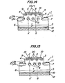
- Fig. 14 is a first modified embodiment of the present invention.
- the first high concentration layer for instance the n layer 4
- the n layer is provided not to have a uniform junction depth over the whole surface region opposite to the cathode electrode 9.
- the n layer is provided to have different junction depth from said side surface 3 of the semiconductor layer 2 viewed from the buried gate region 8 normal to said side surface 3. Namely, at partial area 19 located immediately above the buried gate region 8 is formed as n layer 4' having shallow junction depth and the remaining area is formed as n layer 4 having deep junction depth.
- the junction depth of the first high concentration layer 4 is made uniform.
- the first high concentration layer 4 is made about 10 ⁇ m for the epitaxial grown layer 2b having thickness of 20 ⁇ m.
- the first high concentration layer portion 4' on the line A'-A' is made to have the junction depth about 1-2 ⁇ m, which is some 1/5-1/10 of the junction depth 10 ⁇ m of the first high concentration layer 4 on the line B-B.
- the gate area of the static induction thyristor is about 6-10 times larger compared with the channel area. Therefore, according to this inventive construction, the probability for giving influence against the gate-cathode blocking voltage by the diffusion of n impurity atoms and by an abnormal diffusion at some defect portion is very small, since the portion 4' of the first high concentration layer is made to have shallow junction depth as 1-2 ⁇ m. This will substantially contribute for an improvement for the gate-cathode blocking voltage.
- the emitter injection efficiency of the parasitic n-p-n transistor T 3 in the equivalent circuit diagram of Fig. 3 becomes very small on the line A'-A' compared with that of the conventional construction. Accordingly, the current amplification function of the parasitic n-p-n transistor Tg decreases in accordance with the decreas of the emitter injection efficiency.
- the operation charac - teristic of the static induction transistor T 2 is enhanced due to the decrease of the current-amplification function of the parasitic transistor.
- the static induction thyristor according to the present invention will have much higher dv/dt capability after turn-off compared with the conventional static induction thyristor.
- the distance between the buried gate region 8, which is the p + layer, and the part of first high concentration layer 4' as can be seen on the line A'-A' is longer than the distance between the buried gate region 8 and the first high concentration layer 4 located on the line B-B. Accordingly, the thyristor of this embodiment will have higher gate cathode resistance compared with the conventional thyristor having p + -n-n + junction at the corresponding portion and hence the amount of current is suppressed.
- the static induction thyristor made in accordance with the present invention and having the construction shown in Fig. 14 has a remarkable advantage in that the gate loss at turn-on time is very small under high freqnency operating condition compared with that of the conventional thyristor having construction as shown in Fig. 1.
- oxidized film forming method As the method of selectively forming the subdivided n layer 4 and n + layer 4' on the side surface 3 of the semiconductor layer 2, known methods such as oxidized film forming method, photolithographic method or usual diffusion method can be used.
- the subdivided n layer 4 and n layer 4' at the cathode surface of the semiconductor layer 2 are short-circuited by the aluminium electrode, i.e. the cathode electrode.
- the blocking voltage between the cathode and gate of the thyristor may be limited at some extent by a presence of default in the epitaxial layer.
- FIG. 15 Another embodiment of the present invention shown in Fig. 15 is arranged to improve this gate-cathode blocking voltage.
- this embodiment in the region of semiconductor layer 2 as shown in Fig. 14, namely between the region 19 located immediately above the buried gate region 8 and the cathode electrode 9, there is provided an insulating layer 20 or an insulating film 20.
- This insulating film may be oxide film or nitride film.
- the gate-cathode blocking voltage of the thyristor is improved since the formation of the short circuit between the n layer 4 and the n + layer 4' by the cathode electrode 9 is prevented.
- the current path portion among the total current path extending from the buried gate region 8 to the cathode electrode 9 corresponding to the partial region having only the p +- n junction is insulated so that the current path is substantially bounded only to that portion corresponding to the part of region having p -n-n junction.
- the current path in the Fig. 15 embodiment is narrower than that of the conven - tional construction shown in Fig. -1 and hence the amount of current passing between the gate and cathode of the thyristor decreases remarkably. In other words, the resistance between the gate and cathode of the thyristor becomes higher. Due to this fact the static induction thyristor of the Fig. 15 embodiment has an advantage in that the gate loss at turn-on in high frequency operation is substantially small compared with thyristor having the conventional construction shown in Fig. 1.
- the embodiment shown in Fig. 15 has still further advantage to remarkably improve the manufacturing yield of the thyristor by the improvement of the gate-cathode blocking voltage. This is by the reason that no high concentration layer, namely no n diffusion layer is provided at the region 19 of the semiconductor layer immediately above the buried gate region 8 having substantially larger gate area than the channel area (in practice 1:6-1:10) and that part of the region 19 is inactivated by the provision of the insulating layer 20 so that the occurrence of the fault due to default of the epitaxially grown layer 2b itself can be avoided.
- the selective formation of the insulating layer 20 mentioned in the foregoing can be effected through known technique such as oxidation technique, photolithography or etching.
- Fig. 17 shows still further embodiment of the present invention.
- the dv/dt capability immediately after turn-off of the thyristor in Fig. 14 embodiment can further be improved.
- the construction on cross-seczion along line A'-A' of the Fig. 14 is p + -n-p + -n junction construction (4 layer construction).
- 4 layer construction By the presence of such a 4 layer construction, the dv/dt capability -immediately after turn-off can not be a high amount being the essential feature of the static induction thyristor.
- the construction shown in Fig. 14 had further been modified.
- the second high concentration p layer 6 is made not to be uniform. Namely, viewed from the buried gate region 8 towards the other surface 5 of the semiconductor layer 2, the region 21 located directly below the buried gate region 8 is made to be p layer 6' having shallow junction depth and the other region of the semiconductor layer 2 is made to be p + layer 6 of deep junction depth.
- the region 21 located directly below the buried gate region 8 is made to be p layer 6' having shallow junction depth and the other region of the semiconductor layer 2 is made to be p + layer 6 of deep junction depth.
- the thyristor is made to have the construction in that the buried gate region 8 is oppositely arranged against the anode electrode 10 and the cathode electrode 9 respectively, and that at both regions 19 and 21 of the semiconductor layer located immediately above and below of the buried gate region 8 there is not provided the n layer 4 of the first high concentration layer having deep junction depth and the p + layer 6 of the second high concentration layer having deep junction depth.
- the junction depth of the n layer 4' on the line A'-A' is 1-2 ⁇ m as same as that of Fig. 14 embodiment, the junction depth of n + layer -4 on the line B-B is 10 ⁇ m.
- the junction depth of the p + layer 6' on the line A'-A' is 1-2 ⁇ m and that of the p layer 6 on the line B-B is 15 ⁇ m.
- the junction depth on the line A'-A' is made 1/5-1/10 compared with that on the line B-B.
- the junction depth on the line A'-A' is made 1/7-1/15 compared with that on the line B-B.
- the transistor T 1 (p + -n-p + ) and the parasitic transistor T 3 (n-p + -n + ) on the line A'-A' have much smaller current amplifying function compared with that of the conventional construction shown in Fig. 1. Accordingly, the emitter injection efficiency decreases and the current amplification function decreases.
- the equivalent circuit diagram of this static induction thyristor becomes as shown in Fig. 17.
- This equivalent circuit diagram has just a resistor R connected between the emitter and base of the p-n-p transistor T 1 in addition to the equivalent circuit diagram shown in Fig. 3.
- the ratio of short circuit between the p layer 6, the p + layer 6' and the n layer 21 is about 1 expressed by the surface area of the p + layer and the n layer at the anode surface.
- this thyristor is hardly affected by the influence of the current amplification function since this thyristor is formed of a p-n-p transistor T 1 having suppressed emitter injection efficiency, and a series connection of the static induction transistor T 2 and a parasitic transistor T 3 having less emitter injection efficiency.
- the dv/dt capability immediately after the turn-off can be made high.
- the gate loss at the turn-on of high frequency operation is small just as same as the embodiment shown in Fig. 14.
- n + layer 4 and the n layer 4' on one side surface 3 of the semiconductor layer 2 and the selective formatinn of the p + layer 6 and p + layer 6' on the other side surface 5 in the n layer 2 can be made by using known methods for the formation of oxidized film, -photolithography, diffusion technique, and etc.
- the embodiment shown in Fig. 18 is to further improve the effect of the embodiment shown in Fig. 16.
- insulating layers or insulating films 20 and 20' such as oxide films, nitride films are provided in the semiconductor layer 2, namely between the cathode electrode 9 and the region 19 immediately above the buried gate region 8 and between the anode electrode 10 and the region 21 immediately below the buried gate region 8.
- the current path directly coupling the cathode electrode 9 to n layer 4' located alternately with n layer 4 of the cathode surface forming one side surface 3 of the semiconductor layer 2 is electrically interrupted.
- the blocking voltage between the gate and cathode can further be improved since the formation of the short-circuit between the n layer 4 and the n layer 4' via the cathode electrode 9 is avoided.
- this insulating layer 20 Furthermore, by the insulating action of this insulating layer 20 the operation of the parasitic n-p-n transistor T 3 shown in Fig. 3 is prevented and the equivalent circuit diagram becomes as shown 3n Fig. 2. By this reason, the dv/dt capability immediately after the turn-off of this thyristor of the Tig. 18 embodiment is much larger than that of the conventional thyristor shown in Fig. 1.
- the current path from the buried gate region 8 to the partial region having only p-n junction among the whole current path towards the cathode electrode 9 is insulated and thus the current path is substantially limited to that corresponding to the region having only p + -n-n + junction.
- no such insulating layer interrupting the aforementioned current path is provided. Accordingly, the current path in the thyristor of Fig. 18 embodiment is much narrower than that of the conventional thyristor shown in Fig. 1 and thus the current flowing through the path between the gate and the cathode decreases remarkably. In other words, the resistance between the gate and the cathode of the thyristor becomes high.
- the thyristor of Fig. 18 embodiment has an advantage in that the gate loss at turn-on under high frequency operation is very small compared with the thyristor of the conventional construction shown in Fig. 1.
- the occurrence of default due to defects of the epitaxial growing layer is avoided since the high concentration layer, i.e. the n diffusion layer is not provided at the region 19 of the semiconductor layer 2 located immediately above the buried gate region 8 having the gate area substantially larger than the channel area (in practice 1:6-1:10), and instead an insulating layer 20 is provided at the region 19 and electrically inactivated.
- the gate-cathode blocking voltage the manufacturing yield can be improved very much.
- the second high concentration layer for instance p + layer 6, is formed to have the insulation layer 20' at region 21 immediately below the buried gate region 8 viewing from the gate region 8 towards the other surface 5 of the semiconductor layer 2 normal thereto and to have p layer 6 in the other portion of the semiconductor layer 2.
- the first high concentration layer i.e. n layer 4
- the second high concentration layer i.e.
- n-p + layer 6 and the cross-sectional construction on the line A'-A' is n-p + -n junction structure (3 layer transistor structure). Accordingly, in this embodiment there is no junction having injecting effect at the region 19 and the region 21 of the semiconductor layer located immediately above and below of the buried gate region 8.
- the thyristor in the vertical cross-section is constructed only from an n-p -n transistor and a p + -n-n + diode.
- the p + layer 6 and the n layer 21 are short circuited by the anode electrode for instance aluminium. Accordingly, the equivalent circuit diagram becomes as shown in Fig. 17.
- This circuit has a resistor R connected between the emitter and base of the p-n-p transistor T 2 as shown in the equivalent circuit diagram shown in Fig. 2.
- the short circuit ratio in the area between the p + layer 6 and the n layer 21 is the ratio in the area of p layer and the n layer at the anode surface (area of p layer ⁇ area of n layer). Accordingly, the short circuit ratio becomes comparatively large value of about 6 to 10. Whereas the short circuit ratio of n/p in the conventional device has been less than unity.
- this thyristor consists of a series coupling of a p-n-p transistor T 1 having suppressed emitter injection efficiency and a static induction transistor T 2 . Therefore, this thyristor is hardly affected by the current amplification function, and the dv/dt capability immediately after the turn-off can be made high. Furthermore, the gate loss at the turn-on under high frequency operation is small just as same as the Fig. 14 embodiment.
- the abovementioned selective formation of the insulating layer and the selective diffusion can be made easily through known oxidation technique, photolithography and etching technique.
- the present invention is to improve the characteristics of the static induction thyristor having buried gate structure.
- the invention can equally be applied to a static induction thyristor having low resistance layer (n layer) 22 located between the anode electrode 10 and the n layer in a manner to surround the p layer 6 on the anode surface and the invention will have the same effects with the other embodiment mentioed in the foregoing.
- each of the regions forming the thyristor and the layers and other parts may be the known material in this field of technique.
Landscapes
- Thyristors (AREA)
Applications Claiming Priority (4)
| Application Number | Priority Date | Filing Date | Title |
|---|---|---|---|
| JP185112/83 | 1983-10-05 | ||
| JP58185112A JPS6077463A (ja) | 1983-10-05 | 1983-10-05 | 静電誘導サイリスタ及びその製造方法 |
| JP59007270A JPS60152063A (ja) | 1984-01-20 | 1984-01-20 | 静電誘導サイリスタ |
| JP7270/84 | 1984-01-20 |
Publications (2)
| Publication Number | Publication Date |
|---|---|
| EP0141538A1 true EP0141538A1 (fr) | 1985-05-15 |
| EP0141538B1 EP0141538B1 (fr) | 1988-12-28 |
Family
ID=26341545
Family Applications (1)
| Application Number | Title | Priority Date | Filing Date |
|---|---|---|---|
| EP84306785A Expired EP0141538B1 (fr) | 1983-10-05 | 1984-10-04 | Thyristor à induction statique |
Country Status (3)
| Country | Link |
|---|---|
| US (1) | US4654679A (fr) |
| EP (1) | EP0141538B1 (fr) |
| DE (1) | DE3475859D1 (fr) |
Cited By (3)
| Publication number | Priority date | Publication date | Assignee | Title |
|---|---|---|---|---|
| EP0178582A3 (fr) * | 1984-10-15 | 1989-02-08 | Hitachi, Ltd. | Dispositif semi-conducteur à blocage inverse |
| US5847417A (en) * | 1994-08-26 | 1998-12-08 | Ngk Insulators, Ltd. | Semiconductor device and method of manufacturing same |
| US6163460A (en) * | 1997-10-11 | 2000-12-19 | Temic Telefunken Microelectronic Gmbh | Housing for electronic assemblies including board-mounted components and separate discrete components |
Families Citing this family (11)
| Publication number | Priority date | Publication date | Assignee | Title |
|---|---|---|---|---|
| US5270742A (en) * | 1990-06-07 | 1993-12-14 | Olympus Optical Co., Ltd. | Image forming apparatus for forming electrostatic latent image using ions as medium, with high-speed driving means |
| DE69319465T2 (de) * | 1992-02-20 | 1998-11-12 | Hitachi Ltd | Gate-Turn-Off-Thyristor und dessen Verwendung in Leistungwandlern |
| US5352910A (en) * | 1992-04-07 | 1994-10-04 | Tokyo Denki Seizo Kabushiki Kaisha | Semiconductor device with a buffer structure |
| US5889298A (en) * | 1993-04-30 | 1999-03-30 | Texas Instruments Incorporated | Vertical JFET field effect transistor |
| JPH0855978A (ja) * | 1994-06-09 | 1996-02-27 | Ngk Insulators Ltd | 半導体装置およびその製造方法 |
| JP3214987B2 (ja) * | 1994-09-05 | 2001-10-02 | 日本碍子株式会社 | 半導体装置およびその製造方法 |
| DE19823944A1 (de) * | 1998-05-28 | 1999-12-02 | Siemens Ag | Leistungsdioden-Struktur |
| DE19830332C2 (de) * | 1998-07-07 | 2003-04-17 | Infineon Technologies Ag | Vertikales Halbleiterbauelement mit reduziertem elektrischem Oberflächenfeld |
| JP4990140B2 (ja) * | 2004-08-31 | 2012-08-01 | フリースケール セミコンダクター インコーポレイテッド | パワー半導体デバイス |
| US7353771B2 (en) * | 2005-11-07 | 2008-04-08 | Mks Instruments, Inc. | Method and apparatus of providing power to ignite and sustain a plasma in a reactive gas generator |
| CN101931001B (zh) * | 2009-06-24 | 2012-05-30 | 湖北台基半导体股份有限公司 | 一种非对称快速晶闸管 |
Citations (4)
| Publication number | Priority date | Publication date | Assignee | Title |
|---|---|---|---|---|
| DE3002526A1 (de) * | 1979-01-26 | 1980-08-07 | Zaidan Hojin Handotai Kenkyu | Thyristor der statischen induktionsbauart |
| EP0064561A1 (fr) * | 1980-11-21 | 1982-11-17 | Zaidan Hozin Handotai Kenkyu Shinkokai | Tiristor d'induction statique |
| DE3226327A1 (de) * | 1981-07-14 | 1983-02-03 | Mitsubishi Denki K.K., Tokyo | Halbleitervorrichtung |
| EP0099270A2 (fr) * | 1982-07-13 | 1984-01-25 | Toyo Denki Seizo Kabushiki Kaisha | Procédé pour la formation d'électrodes de porte enterrées pour un dispositif semi-conducteur |
Family Cites Families (8)
| Publication number | Priority date | Publication date | Assignee | Title |
|---|---|---|---|---|
| JPS53118982A (en) * | 1977-03-28 | 1978-10-17 | Seiko Instr & Electronics Ltd | Electrostatic induction transistor logic element |
| JPS54106176A (en) * | 1978-02-08 | 1979-08-20 | Hitachi Ltd | Field effect switching element |
| US4364072A (en) * | 1978-03-17 | 1982-12-14 | Zaidan Hojin Handotai Kenkyu Shinkokai | Static induction type semiconductor device with multiple doped layers for potential modification |
| US4345266A (en) * | 1978-07-20 | 1982-08-17 | General Electric Company | Transistor having improved turn-off time and second breakdown characteristics with bi-level emitter structure |
| JPS6016753B2 (ja) * | 1979-01-19 | 1985-04-27 | 株式会社日立製作所 | 半導体スイツチング素子およびその制御方法 |
| JPS566471A (en) * | 1979-06-28 | 1981-01-23 | Meidensha Electric Mfg Co Ltd | Field effect type thyristor |
| JPS6011815B2 (ja) * | 1979-07-09 | 1985-03-28 | 三菱電機株式会社 | サイリスタ |
| CA1154879A (fr) * | 1980-11-17 | 1983-10-04 | Yoshinori Yukimoto | Redresseur commande par un semiconducteur |
-
1984
- 1984-10-01 US US06/656,581 patent/US4654679A/en not_active Expired - Fee Related
- 1984-10-04 DE DE8484306785T patent/DE3475859D1/de not_active Expired
- 1984-10-04 EP EP84306785A patent/EP0141538B1/fr not_active Expired
Patent Citations (4)
| Publication number | Priority date | Publication date | Assignee | Title |
|---|---|---|---|---|
| DE3002526A1 (de) * | 1979-01-26 | 1980-08-07 | Zaidan Hojin Handotai Kenkyu | Thyristor der statischen induktionsbauart |
| EP0064561A1 (fr) * | 1980-11-21 | 1982-11-17 | Zaidan Hozin Handotai Kenkyu Shinkokai | Tiristor d'induction statique |
| DE3226327A1 (de) * | 1981-07-14 | 1983-02-03 | Mitsubishi Denki K.K., Tokyo | Halbleitervorrichtung |
| EP0099270A2 (fr) * | 1982-07-13 | 1984-01-25 | Toyo Denki Seizo Kabushiki Kaisha | Procédé pour la formation d'électrodes de porte enterrées pour un dispositif semi-conducteur |
Cited By (4)
| Publication number | Priority date | Publication date | Assignee | Title |
|---|---|---|---|---|
| EP0178582A3 (fr) * | 1984-10-15 | 1989-02-08 | Hitachi, Ltd. | Dispositif semi-conducteur à blocage inverse |
| US5847417A (en) * | 1994-08-26 | 1998-12-08 | Ngk Insulators, Ltd. | Semiconductor device and method of manufacturing same |
| US6159776A (en) * | 1994-08-26 | 2000-12-12 | Ngk Insulators, Ltd. | Method for manufacturing semiconductor device |
| US6163460A (en) * | 1997-10-11 | 2000-12-19 | Temic Telefunken Microelectronic Gmbh | Housing for electronic assemblies including board-mounted components and separate discrete components |
Also Published As
| Publication number | Publication date |
|---|---|
| DE3475859D1 (en) | 1989-02-02 |
| US4654679A (en) | 1987-03-31 |
| EP0141538B1 (fr) | 1988-12-28 |
Similar Documents
| Publication | Publication Date | Title |
|---|---|---|
| US4223328A (en) | Field controlled thyristor with dual resistivity field layer | |
| US5506427A (en) | Heterojunction bipolar transistor with silicon-germanium base | |
| US4145703A (en) | High power MOS device and fabrication method therefor | |
| US5468654A (en) | Method of manufacturing an insulated gate bipolar transistor | |
| US5637889A (en) | Composite power transistor structures using semiconductor materials with different bandgaps | |
| US4654679A (en) | Static induction thyristor with stepped-doping gate region | |
| US5557118A (en) | Hetero-junction type bipolar transistor | |
| US4499657A (en) | Method of making a semiconductor device having protected edges | |
| US4137109A (en) | Selective diffusion and etching method for isolation of integrated logic circuit | |
| US4514747A (en) | Field controlled thyristor with double-diffused source region | |
| KR100289473B1 (ko) | 다층 베이스 헤테로접합 장치 및 그 제조방법 | |
| JPH0347593B2 (fr) | ||
| EP0099270B1 (fr) | Procédé pour la formation d'électrodes de porte enterrées pour un dispositif semi-conducteur | |
| EP0609351A1 (fr) | Transistor bipolaire presentant des caracteristiques ameliorees de gain en courant et de claquage | |
| EP0615292A1 (fr) | Transistor bipolaire à grille isolée | |
| JPH0712057B2 (ja) | トランジスタ及びその製造方法 | |
| US4901131A (en) | Conductivity modulated metal oxide semiconductor field effect transistor | |
| JPH065789A (ja) | 埋込みドレイン又はコレクタ領域形成方法 | |
| EP0756760B1 (fr) | Dispositif a semiconducteur a anneau de garde, et son procede de fabrication | |
| US6114212A (en) | Methods of fabricating bipolar junction transistors having an increased safe operating area | |
| US4067036A (en) | Junction field effect transistor of vertical type | |
| EP0157207A2 (fr) | Thyristor à commande d'extinction | |
| EP0845813A1 (fr) | Transistor bipolaire à grille isolée | |
| US5221856A (en) | Bipolar transistor with floating guard region under extrinsic base | |
| KR19990065744A (ko) | 콜렉터와 에미터 사이에 다이오드를 내장한 바이폴라 트랜지스터 및 그 제조방법 |
Legal Events
| Date | Code | Title | Description |
|---|---|---|---|
| PUAI | Public reference made under article 153(3) epc to a published international application that has entered the european phase |
Free format text: ORIGINAL CODE: 0009012 |
|
| AK | Designated contracting states |
Designated state(s): CH DE GB LI SE |
|
| 17P | Request for examination filed |
Effective date: 19851102 |
|
| 17Q | First examination report despatched |
Effective date: 19860708 |
|
| D17Q | First examination report despatched (deleted) | ||
| GRAA | (expected) grant |
Free format text: ORIGINAL CODE: 0009210 |
|
| AK | Designated contracting states |
Kind code of ref document: B1 Designated state(s): CH DE GB LI SE |
|
| REF | Corresponds to: |
Ref document number: 3475859 Country of ref document: DE Date of ref document: 19890202 |
|
| PLBE | No opposition filed within time limit |
Free format text: ORIGINAL CODE: 0009261 |
|
| STAA | Information on the status of an ep patent application or granted ep patent |
Free format text: STATUS: NO OPPOSITION FILED WITHIN TIME LIMIT |
|
| 26N | No opposition filed | ||
| EAL | Se: european patent in force in sweden |
Ref document number: 84306785.1 |
|
| PGFP | Annual fee paid to national office [announced via postgrant information from national office to epo] |
Ref country code: GB Payment date: 19950925 Year of fee payment: 12 |
|
| PGFP | Annual fee paid to national office [announced via postgrant information from national office to epo] |
Ref country code: SE Payment date: 19951017 Year of fee payment: 12 |
|
| PGFP | Annual fee paid to national office [announced via postgrant information from national office to epo] |
Ref country code: CH Payment date: 19951030 Year of fee payment: 12 |
|
| PGFP | Annual fee paid to national office [announced via postgrant information from national office to epo] |
Ref country code: DE Payment date: 19951130 Year of fee payment: 12 |
|
| PG25 | Lapsed in a contracting state [announced via postgrant information from national office to epo] |
Ref country code: GB Effective date: 19961004 |
|
| PG25 | Lapsed in a contracting state [announced via postgrant information from national office to epo] |
Ref country code: SE Effective date: 19961005 |
|
| PG25 | Lapsed in a contracting state [announced via postgrant information from national office to epo] |
Ref country code: LI Effective date: 19961031 Ref country code: CH Effective date: 19961031 |
|
| GBPC | Gb: european patent ceased through non-payment of renewal fee |
Effective date: 19961004 |
|
| REG | Reference to a national code |
Ref country code: CH Ref legal event code: PL |
|
| PG25 | Lapsed in a contracting state [announced via postgrant information from national office to epo] |
Ref country code: DE Effective date: 19970701 |
|
| EUG | Se: european patent has lapsed |
Ref document number: 84306785.1 |