EP0142171A2 - Circuit de comparaison de fréquences - Google Patents
Circuit de comparaison de fréquences Download PDFInfo
- Publication number
- EP0142171A2 EP0142171A2 EP84113778A EP84113778A EP0142171A2 EP 0142171 A2 EP0142171 A2 EP 0142171A2 EP 84113778 A EP84113778 A EP 84113778A EP 84113778 A EP84113778 A EP 84113778A EP 0142171 A2 EP0142171 A2 EP 0142171A2
- Authority
- EP
- European Patent Office
- Prior art keywords
- frequency
- signal
- circuit
- voltage
- output
- Prior art date
- Legal status (The legal status is an assumption and is not a legal conclusion. Google has not performed a legal analysis and makes no representation as to the accuracy of the status listed.)
- Granted
Links
- 239000003990 capacitor Substances 0.000 claims abstract description 69
- 239000002131 composite material Substances 0.000 claims abstract description 36
- 230000010354 integration Effects 0.000 claims description 4
- 230000001360 synchronised effect Effects 0.000 claims description 4
- 238000010586 diagram Methods 0.000 description 22
- 238000010276 construction Methods 0.000 description 11
- 238000001514 detection method Methods 0.000 description 2
- 238000005516 engineering process Methods 0.000 description 2
- 230000004048 modification Effects 0.000 description 2
- 238000012986 modification Methods 0.000 description 2
- 230000005236 sound signal Effects 0.000 description 2
- 230000015572 biosynthetic process Effects 0.000 description 1
- 239000013078 crystal Substances 0.000 description 1
- 230000007423 decrease Effects 0.000 description 1
- 230000000593 degrading effect Effects 0.000 description 1
- 230000003111 delayed effect Effects 0.000 description 1
- 230000000694 effects Effects 0.000 description 1
- 230000000630 rising effect Effects 0.000 description 1
- 230000000087 stabilizing effect Effects 0.000 description 1
- 238000003786 synthesis reaction Methods 0.000 description 1
Images


Classifications
-
- H—ELECTRICITY
- H03—ELECTRONIC CIRCUITRY
- H03K—PULSE TECHNIQUE
- H03K4/00—Generating pulses having essentially a finite slope or stepped portions
- H03K4/02—Generating pulses having essentially a finite slope or stepped portions having stepped portions, e.g. staircase waveform
- H03K4/023—Generating pulses having essentially a finite slope or stepped portions having stepped portions, e.g. staircase waveform by repetitive charge or discharge of a capacitor, analogue generators
-
- G—PHYSICS
- G01—MEASURING; TESTING
- G01R—MEASURING ELECTRIC VARIABLES; MEASURING MAGNETIC VARIABLES
- G01R23/00—Arrangements for measuring frequencies; Arrangements for analysing frequency spectra
- G01R23/005—Circuits for comparing several input signals and for indicating the result of this comparison, e.g. equal, different, greater, smaller (comparing phase or frequency of 2 mutually independent oscillations in demodulators)
-
- G—PHYSICS
- G10—MUSICAL INSTRUMENTS; ACOUSTICS
- G10L—SPEECH ANALYSIS TECHNIQUES OR SPEECH SYNTHESIS; SPEECH RECOGNITION; SPEECH OR VOICE PROCESSING TECHNIQUES; SPEECH OR AUDIO CODING OR DECODING
- G10L19/00—Speech or audio signals analysis-synthesis techniques for redundancy reduction, e.g. in vocoders; Coding or decoding of speech or audio signals, using source filter models or psychoacoustic analysis
- G10L19/02—Speech or audio signals analysis-synthesis techniques for redundancy reduction, e.g. in vocoders; Coding or decoding of speech or audio signals, using source filter models or psychoacoustic analysis using spectral analysis, e.g. transform vocoders or subband vocoders
-
- H—ELECTRICITY
- H03—ELECTRONIC CIRCUITRY
- H03K—PULSE TECHNIQUE
- H03K3/00—Circuits for generating electric pulses; Monostable, bistable or multistable circuits
- H03K3/02—Generators characterised by the type of circuit or by the means used for producing pulses
- H03K3/023—Generators characterised by the type of circuit or by the means used for producing pulses by the use of differential amplifiers or comparators, with internal or external positive feedback
- H03K3/0231—Astable circuits
Definitions
- the present invention relates to a frequency comparing circuit which compares two frequency signals.
- an impulse and a white noise are used as a sound source.
- the signal from the sound source is passed through several digital filters to obtain an audio signal.
- the conditions for the digital filters depend on the audio signal to be achieved.
- the conditions for the digital filters in the digital speech synthesizer are set by analyzing and recognizing an actual voice.
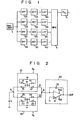
- Fig. 1 is a conventional block diagram of a speech recognition circuit.
- a mike amplifier 1 amplifies an analog signal from a microphone (not shown).
- the output from the mike amplifier 1 is supplied in parallel to, for example, four band-pass filters (BPF) 2A, 2B, 2C and 2D.
- BPF band-pass filters
- the signals which pass through the four band-pass filters 2A, 2B,-2C and 2D are detected by four detectors, respectively.
- the detected four signals are supplied to four low-pass filter circuits 4A, 4B, 4C and 4D, respectively.
- the signals which pass through the low-pass filter circuits 4A, 4 B , 4C and 4D are selectively supplied to an analog/digital converter (A/D) 6 through a multiplexer 5.
- A/D analog/digital converter
- the digital output from the analog/digital converter 6 results in a recognition result for the voice input through the microphone.
- the employment of switched-capacitor filter technology introduces higher integration and higher accuracy to the recent speech recognition circuit.
- the mike amplifier 1, band-pass filter circuits 2A through 2D and low-pass filter circuits 4A through 4D all adopt the switched capacitor circuit.
- any circuit which uses such a switched capacitor circuit is required to include an oscillator and a clock generator which produces various clock pulses from the oscillator output.
- the actual oscillating frequency can be matched to the accurate oscillating frequency by knowing whether the actual oscillating frequency is greater or smaller than the accurate oscillating frequency, or the fluctuation or ratio between the actual oscillating frequency and the accurate oscillating frequency.
- a PLL (phase locked loop) circuit has been known as a means for accurately detecting which frequency is greater or smaller, or the fluctuation or ratio between the actual and accurate frequencies.
- the PLL circuit is not adapted to integration due to its complicated construction. Therefore, with prior art circuits with simplified constructions, an accurate oscillating frequency can not be obtained, thereby degrading the switched capacitor circuit which leads to a speech recognition circuit with poor accuracy.
- Another object of the invention is to provide a simply constructed frequency comparing circuit which can detect with high accuracy a fluctuation between two frequency signals.
- a further object of the invention is to provide a frequency-voltage converting circuit which can stably generate with high accuracy an arbitrary multiple of frequencies from the reference signal derived from an oscillating signal: the oscillating signal comes from an oscillator such as a crystal oscillator which stably oscillates.
- a frequency comparing circuit comprising:
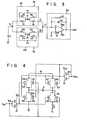
- Fig. 2 is a circuit diagram showing an embodiment of a frequency comparing circuit of the present invention.
- the switched capacitor circuit 10 comprises a capacitor 11 and four switches 12 through 15.
- the circuit 10 has a negative equivalent resistance, and its value is determined corresponding to the frequency f s of an oscillating signal S from an oscillator.
- One terminal of each switch 12 and 13 is connected to one terminal of the capacitor 11, and the other terminal of the switch 12 is grounded.
- the other terminal of the capacitor 11 is connected to one terminals of the switches 14 and 15, and the other terminal of the switch 14 is grounded.
- the switched capacitor circuit 20 comprises a capacitor 21 and four switches 22 through 25 and has a positive equivalent resistance, the value of which is determined corresponding to a reference signal S c with frequency f c .
- One terminal of the capacitor 21 is connected to one terminal of each switch 22 and 23, and the other terminal of the switch 23 is grounded.
- the other terminal of the capacitor 21 is connected to one termianl of each switch 24 and 25, and the other terminal of the switch 25 is grounded.
- a switch pair 22 and 24 and another switch pair 23 and 25 are alternatively turned on in response to a signal S c .
- the other terminal of the switch 13 in the switched capacitor circuit 10 and the other terminal of the switch 22 in the switched capacitor circuit 20 are connected at a common connection a. Futhermore, the positive electrode of a DC power source V is connected to the common connection a. The negative electrode of the DC power source V is grounded. Also, the other terminals of the switch 15 in the switched capacitor circuit 10 and the switch 24 in the switched capacitor ! circuit 20 are connected to a common connection b. Furthermore, an input terminal of an integrator 30 is connected to the common connection b.
- the integrator 30 is provided with a differential amplifier 31 having an inverted input terminal, a non-inverted input terminal and output terminal, and a capacitor 32.
- the capacitor 32 is connected between the inverted input terminal and output terminal, and the non-inverted input terminal of the differential amplifier 31 is grounded.
- the differential amplifier 31 operates at a voltage between a positive electrode voltage V and a negative electrode voltage V SS .
- the ground voltage is set at an intermediate potential between the positive and negative voltage, for example, at 0 V.
- the inverted input terminal of the differential amlifier 31 serves as the input terminal of the integrator 30.
- the integrator 30 produces on its output terminal a signal OUT corresponding to the magnitude relation between two frequencies f and f .
- the equivalent resistance R 1 of the switched capacitor circuit 10 (hereafter referred to as SC circuit) is given by: wherein C 1 represents the capacitance of the capacitor 11.
- the equivalent resistance R 2 of the SC circuit 20 is given by: wherein C 2 represents the capacitance of the capacitor 21.
- each two SC circuits 10 and 20 As the one terminal of each two SC circuits 10 and 20, namely, the other terminals of the switches 13 and 22 are connected through the connection a to the positive electrode of the DC power source V, the positive bias from the DC power source V is supplied to both SC circuits 10 and 20. Therefore, a predetermined DC current flows into the respective SC circuits 10 and 20.
- the SC circuit 10 has negative equivalent resistance R 1
- the direction of the current I 1 is to the left in Fig. 2.
- the SC circuit 20 has a positive equivalent resistance R 2
- the direction of the current I 2 is to the right in Fig. 2.
- the directions of the currents I 1 and I 2 are opposite to each other.
- a composite current of I 1 and I 2 is supplied to the integrator 30.
- the output signal OUT of the integrator 30 becomes ground voltage.
- I 1 > I 2 and current corresponding to the difference between I 1 and I 2 flows from the integrator 30 the level of the output signal OUT of the integrator 30 becomes high (V DD level).
- I 2 > I 1 and current corresponding to the difference between I 1 and I 2 flows into the integrator 30 the level of the output signal OUT of the integrator 30 become low (V SS level).
- the output signal OUT of the integrator 30 becomes ground voltage. Furthermore, when the frequency f s is greater than the frequency f , the level of the output signal OUT of the integrator 30 becomes high. On the other hand, when the frequency f c is smaller than the frequency f c , the level of the output signal OUT of the integrator 30 becomes low. In summary, the output signal OUT of the integrator 30 varies its level according to the cyclical relationship of the two frequencies f and f c . Therefore, the comparison of the two frequencies can be performed by determining the output signal OUT.
- the equivalent resistances R 1 and R 2 of the SC circuits 10 and 20 are determined only by the frequencies f s and f , provided that the capacitances C 1 and C2 are constant as shown in the equations (1) and (2). Since the capacitances C 1 and C 2 can be set with a relatively higher accuracy than the resistances, the respective frequencies f s and f c can be converted into the resistances R 1 and R 2 with high accuracy. Furthermore, the integrator 30 achieves the signal OUT by integrating the composite values of flowing currents corresponding to the resistances R 1 and R 2 . Thus, the comparison between f s and f c can be performed with high accuracy even if the slew rate or gain of the differential amplifier 31 fluctuates.
- the comparison and detection can be performed with high accuracy on the cyclical relationship between the frequency f s of the oscillating signal S s from-the oscillator and the frequency f c of the reference signal S . Therefore, the frequency f can be matched with the reference frequency f with high accuracy by using the output signal OUT.
- Fig. 3 is a circuit diagram showing a construction of another embodiment of the frequency comparing circuit of the invention.
- the circuit in Fig. 3 is same as that in Fig. 2 except that a resistor 33 is connected in parallel to the capacitor 32 in the integrator 30.
- the output signal OUT is set to ground voltage.
- the output signal OUT is set to less than the V DD or V SS level in accordance with the electrode of the composite current.
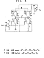
- Figs. 4 and 5 show detailed circuits of the SC circuits 10 and 20 used in the above embodiment, respectively.
- the same numerals as in Figs. 2 and 3 are used for the same parts in Figs. 4 and 5.
- two signals S sl and S s2 or S c1 and S c2 are used whose phases are different than each other as shown in the timing charts of Figs. 6A and 6B.
- the switches 12 through 15 in the SC circuit 10 having negative resistance comprise, as shown in Fig. 4, C M OS switches 52 through 55 in which N channel MOSFETs 41 through 44 and P channel MOSFETs 45 through 48 are connected in parallel to each other.
- the signal S sl in Fig. 6A is supplied to the gates of the N channel MOSFETs 41 and 44 and through a CMOS inverter 49 to the gates of the P channel MOSFETs 45 and 48.
- the signal S s2 in Fig. 6B is supplied to the gates of the N channel MOSFETs 42 and 43 and through a CMOS inverter 50 to the gates of the P channel MOSFETs 46 and 47.
- the switching control of the CMOS switches 52 through 55 will be described in response to the signals S sl and S s2 under the condition that the DC voltage V1 is supplied to the other terminal of the CMOS switch 53 and the other terminal of the CMOS switch 55 is grounded.
- the level of the signal S s2 is high, the CMOS switches 53 and 54 turn on.
- the other terminal (point C in Fig. 4) of the capacitor 11 will be charged at -C ⁇ V 1 .
- the CMOS switches 52 and 55 turn on. At this time, the positive charge +C 1 ⁇ V 1 from the ground is supplied through the CMOS switch 55 to the point C so as to cancel the negative charge at the point C.
- the value of the current I which flows in the SC circuit is given by:
- the equivalent resistance R in the SC circuit 10 is obtained by dividing the current I by the supply voltage Vl.
- the equivalent resistance R is given by:
- the right side in the equation (4) is the same as the right side in equation (1). Therefore, the equation (4) reveals that the SC circuit 10 in Fig. 4 has the negative equivalent resistance corresponding to the frequency f .
- the switches 22 through 25 in the SC circuit 20 comprise the CMOS switches 72 through 75 in which N channel MOSFETs 61 through 64 and P channel MOSFETs 65 through 68 are connected in parallel, respectively, as shown in Fig. 5.
- the signal S cl in Fig. 6A is supplied to the gates of the N channel MOSFETs 61 and 63 and through the CMOS inverter 69 to the gates of the P channel MOSFETs 65 and 67.
- the signal S c2 in Fig. 6B is supplied to the gates of the N channel MOSFETs 62 and 64 and through a CMOS inverter 70 to the P channel MOSFETs 66 and 68.
- the equivalent resistance R in the SC circuit is obtained by dividing the supply voltage V2 by the current I. That is:
- the right side in equation (6) is the same as that in equation (2).
- the equation (6) reveals that the SC circuit 20 in Fig. 5 has a positive equivalent resistance corresponding to the frequency f .
- Fig. 7 is a circuit diagram showing an applied construction of the invention.
- the circuit of this application comprises two frequency comparing circuits 100 and 200 constructed like those in Fig. 2 and an AND gate 300 which receives both the output signals OUT1 and OUT2.
- the SC circuit having the negative equivalent resistance (referred to by 10 in Fig. 2) in one frequency comparing circuit 100 is controlled by a signal S ca having a higher reference frequency f ca .
- the SC circuit having a positive equivalent resistance (referred to by 20 in Fig. 2) is controlled by a signal S s having a frequency f s to be compared.
- the SC circuit having a negative equivalent resistance (referred by 10 in Fig. 2) in the frequency comparing circuit 200 is controlled by a signal S cb having a lower frequency f and the SC circuit having a positive equivalent resistance is controlled by the signal S .
- the circuit can detect whether the frequency f s to be compared is between the higher reference frequency f ca and the lower reference frequency signal f cb .
- a common DC power source V is used to flow DC current in the SC circuits 10 and 20.
- different DC power sources may be used for the SC circuits 10 and 20.
- the apparent frequency of the reference signals S c can be varied from the actual frequency f c by using different DC power sources as changing values of the capacitors 11 and 21.
- one SC circuit 10 having a negative equivalent resistance is controlled by the signal S s
- the other SC circuit 20 having a positive equivalent resistance is controlled by the signal S.
- the signals Sand S are interchangeable.
- Fig. 8 shows an embodiment of the frequency comparing circuit which can perform fluctuations between the two signal's frequencies with high accuracy.
- the same numerals are used for the same parts in Fig. 2 and the descriptions are omitted.
- two resistors 76 and 77 are connected in series between the positive electrode power source V DD and the ground.
- the other terminal of the switch 13 in the switched capacitor circuit 10 is connected to a serial connection al between the resistors 76 and 77.
- two resistors 78 and 79 are serially connected between V DD and the output point OUT of voltage V 0 .
- the other terminal of the switch 22 of the SC circuit 20 is connected at the serial connection a2 between the resistors 78 and 79.
- the differential amplifier 31 operates at a voltage between the positive electrode power source voltage V DD and negative electrode power source voltage V SS whose absolute value is equal that of V DD .
- the ground potential is set between V DD and V SS , for example, to 0 V .
- the inverted input terminal of the differential amplifier 31 serves as the input terminal, and from the output terminal, voltage proportional to the fluctuation between the two frequencies f s and f c is provided.
- a constant positive voltage V 1 determined by the resistance ratio of the resistors 76 and 77, and the voltage V DD is supplied to the connection al where the one terminal of the SC circuit 10, that is, the other terminal of the switch 13, is connected.
- the equivalent resistance R 1 of the SC circuit 10 becomes negative as in the equation (1) if the value of the capacitor 11 is C 1 .
- the direction of the current I 1 flowing into the SC circuit 10 is to the left in Fig. 8.
- Positive or negative voltage V 2 determined by the resistance ratio of the resistors 78 and 79, voltage V DD , and the output voltage V from the integrator 30, is supplied to the connection a2 where one terminal of the SC circuit 20, that is, the other terminal of the switch 22, is connected.
- the equivalent resistance R 2 of the SC circuit 20 becomes positive as in the equation (2) if the value of the capacitor 21 is C 2 .
- the integrator 30 integrates the composite current of I 1 and I 2 and reduces voltage V 0 .
- the output voltage V 0 When the output voltage V 0 is ground voltage, the voltage V 2 at the connection a2 becomes (V DD -0)/2 as the values of the resistors 78 and 79 are equal. Also, the voltage V 1 at the connection al becomes (V DD -0)/2 as the values of the resistors 76 and 77 are equal. Therefore, voltage V 1 is equal to voltage V 2 .
- the output voltage V 0 of the integrator 30 becomes ground voltage (0 V) when the frequency f s coincides with the frequency f c .
- the voltage V 2 at the connection a2 becomes (V DD -0)/2 as the values of the resistors 78 and 79 are equal.
- the voltage V 1 at the connection al becomes (VDD-0)/2 as the values of the resistors 76 and 77 are equal. Therefore, voltage V 1 is equal to voltage V2 .
- the output voltage V 0 of the integrator 30 is fixed at the ground level when the frequency f s coincides with the frequency f c .
- the equivalent resistance of the SC circuit 10 given by the equation (1) becomes greater. Since the value of voltage V 1 supplied to the SC circuit 10 is constant, the greater the resistance R 1 , the smaller the current value I 1 . As a result, the composite current of I 1 and I 2 becomes positive (in the direction of flowing into the integrator 30).
- the integrator 30 integrates the composite current and produces negative voltage V 0 proportional to the current.
- the voltage V0 serves to lower the voltage V 2 at the connection a2, so that the value of the current flowing in the SC circuit 20 becomes smaller.
- the output voltage V0 of the integrator 30 becomes constant.
- the frequency f s of the oscillating signal S s is measured on the abscissa
- the output voltage V 0 of the integrator 30 is measured on the ordinate.
- the frequency f s fluctuates corresponding to a voltage higher than the frequency f c
- the frequency f s fluctuates corresonding to a voltage lower than the frequency f c
- the equivalent resistances R 1 and R 2 in the SC circuits 10 and 20 depend, as is shown in the equations (1) and (2), only on the frequencies f s and f c if the values of C 1 and C 2 are constant, respectively. Therefore, the values of the capacitors C 1 and C 2 can be set with relatively higher accuracy compared to those of the resistors. Thus, the frequencies f s and f c can be converted into equivalent resistances R 1 and R 2 with higher accuracy.
- the apparent frequency of the reference signal S c can be varied from the actual frequency f c by setting the values C 1 and C 2 of the capacitors 11 and 21 and values of resistors 76 and 79.
- the applicant has conducted an experiment where 100PF is selected for C 1 and C 2 , +7V for V DD , -7V for V SS and 2KHz, 4KHz and 8KHz for f c , respectively.
- the output voltage V 0 represents linear characteristic when the frequency f s is in the range of O.lfc through 1.7 or 1.8fc.
- Fig. 10 is a circuit diagram showing an applied construction of the invention.
- the application circuit is constructed in such a way that the output voltage V 0 of a frequency comparing circuit 400, constructed as in Fig. 8, is supplied to an inverter 500, thereby to obtain a logic signal OUT with either a high or low level set according to the voltage V 0 .
- Figs. 11A and 11B are circuit diagrams showing a construction of an embodiment of the oscillating circuit in Fig. 10. In the figures, the same numerals are used for the same parts in Fig. 2, thereby to omit the description thereof.
- the output of the integrator 30 is supplied through a voltage buffer circuit 80 to a Schmitt-type oscillator 83.
- the voltage buffer circuit 80 comprises a differential amplifier 81 with an inverted input terminal, non-inverted input terminal and output terminal. The inverted input terminal is connected to the output terminal. The inverted input terminal is supplied with the voltage V 0 .
- the Scmitt-type oscillator 83 is provided with a differential amplifier 84 with a non-inverted input terminal, inverted input terminal and output terminal.
- a higher level threshold voltage V H and lower-level threshold voltage VL are alternatively supplied to the non-inverted input.terminal of the differential amplifier 84.
- the higher level threshold voltage V H is obtained at the serial connection c of the two resistors 85 and 86 serially connected at the point between the positive power supply voltage V DD and the output terminal of the voltage buffer circuit 80.
- the voltage V H is input to the non-inverted input terminal of the differential amplifier 84 through a CMOS switch 89 which comprises the P-channel MOSFET 87 and N-channel MOSFET 88.
- the lower level threshold voltage V L is obtained at the serial connection d of the resistors 90 and 91 serially connected between the point at which the positive power supply voltage V DD is applied and the point at which the negative power supply voltage V SS is applied.
- the voltage V L is input to the non-inverted input terminal of the differential amplifier 84 through a CMOS switch 94 which comprises the P channel MOSFET 92 and N channel MOSFET 93.
- DC voltage V V1 is applied to the point al of the switched capacitor circuit 10
- variable DC voltage V V2 is applied to the point a2 of the switched capacitor circuit 20.
- Two inverters 95 and 96 are cascade-connected to the output terminal of the differential amplifier 84, and a resistor 97 and a capacitor 98 are serially connected between the output terminal of the inverter 96 in the lower stream and the point at which the voltage V SS is applied.
- the output signal of the inverter 96 is input in parallel to a gate of an N-channel MOSFET 88 which constitutes the CMOS switch 89 and a gate of a P-channel MOSFET 92 which constitutes the CMOS switch 94 as well as to two inverters 99 and 101.
- the output signal of the inverter 99 is supplied in parallel to a gate of a P-channel MOSFET 87 which constitutes the CMOS switch 89 and a gate of an N-channel MOSFET 93 which constitutes the CMOS switch 94. Furthermore, a voltage at the point e where the resistor 97 and the capacitor 98 are serially connected is input to the inverted input terminal of the differential amplifier 84. The output signal of the inverter 101 is supplied to another circuit as the oscillating output signal S s and is fed back to the SC circuit 10 through a line 102.
- the three differential amplifiers 31, 81 and 84 operate at a voltage between the positive power supply voltage V DD and the negative power supply voltage whose absolute value is equal to V DD .
- the voltage at the ground is set to 0 V which is intermediate between V DD and V SS'
- the operation of the Schmitt-type oscillating circuit 83 in the embodiment will first be described.
- the resistance ratio of the resistors 85 and 86 and the threshold voltage V H obtained at the point c corresponding to the output voltage V 0 from the voltage buffer amplifier 80 are fixed, and that the voltage VH is higher than the threshold voltage V L obtained at the point d corresponding to the resistance ratio of the resistors 90 and 91.
- the level of the output signal of the differential amplifer 84 is high (V DD level)
- the level of the output signal of the inverter 96 becomes high, so that the capacitor 98 discharges through the resistor 97 at the time constant T corresponding to the resistor 97 and the capacitor 98.
- the voltage at the point e raises gradually.
- the CMOS switch 89 turns on. Therefore, a high level threshold voltage V H is input to the non-inverted input terminal of the differential amplifier 84.
- the differential amlifier 84 compares the threshold voltage V H and the voltage at the point e. When the voltage at the point e reaches the threshold voltage V H , the output signal of the differential amplifier 84 is inverted from a high level to a low level (V SS level). After the level inversion, the output signal of.the inverter 96 is also inverted into two levels, and the capacitor 98 which has been charged now discharges with the time constant T to the V SS level through the resistance 97.
- the differential amplifier 84 compares the threshold value V L with the voltage at the point e. As a result, the lowering voltage at the point e reaches the threshold value V L , and the output signal of the differential amplifier 84 is again inverted to a high level. As described above, the differential amplifier 84 alternatively compares the voltage at the point e with the threshold voltage V B and the threshold voltage V L .
- the output signal of the inverter 96 becomes an oscillating signal in which a high level and a low level are repeated alternatively.
- the output signal S s of the inverter 101 is also the oscillating signal as it is the inverted signal through the inverter 96.
- the frequency f s of the oscillating signal S s of the Schmitt-type oscillator 83 is constant when the threshold voltages V H and V L are constant.
- the value f s corresponds to the Schmitt width (
- Fig. 12 is a waveform showing the relation of the voltage V e at the point e and the output voltage S s of the inverter 96.
- the equivalent resistance R 1 of the SC circuit 10, to which the oscillating signal S s from the Schmitt-type oscillating circuit 83 is input, is given by the equation (1) when the value of the capacitor 11 is C 1 , as shown in Fig. 2.
- the positive voltage from the DC power supply V 1 or variable DC power supply V2 is supplied to one terminal of the SC circuits 10 and 20, that is, the other terminal of the switch 13 in the SC circuit 10 and the other terminal of the switch 22 in the SC circuit 20, direct current flows in the SC circuits 10 and 20, respectively.
- the SC circuit 10 has a negative equivalent resistance R 1
- the direction of the current I 1 flowing in the SC circuit 10 is to the left (negative direction) in Figs. 11A and 11B.
- the direction of the current I 2 flowing in the SC circuit 20 is to the right (positive direction) in Figs. 11A and 11B.
- the directions of I 1 and I 2 are opposite to each other.
- the composite current of T 1 and I 2 is supplied to the integrator 30. When the composite current is negative, that is, the current I 1 is greater than the current I 2 , the output voltage V 0 of the integrator 30 rises gradually to the positive power supply voltage VDD.
- the value of the DC power supply V 1 and the value of the variable DC power supply,V 2 are equally set, and the values C l and C 2 of the capacitors 11 and 12 in the SC circuits 10 and 20 are equally set. Then, in the SC circuits 10 and 20 the composite current of I 1 and I 2 becomes 0, and the output voltage V 0 of the integrator 30 is fixed to some value when the coincidence between the frequecies f s and f c of the signals S s and S c is achieved.
- value V 0 is fixed, the higher threshold voltage V H formed in the Schmitt-type oscillator 83 is fixed, thereby fixing the Schmitt width (
- the composite value of the current I and I 2 increases toward 0 from negative and becomes 0 when f s coincides with f.
- the output voltage V 0 of the integrator 30 lowers toward V ss until f s coincides with f c .
- the output voltage V 0 becomes its original value, the lowering of the voltage ceases.
- lowering of the frequency f s is also ceased when the frequency fsof the oscillating output signal S S coincides with f c .
- the frequency f s of the oscillating output signal S s is controlled so as to coincide with the frequency f c of the signal S .
- variable DC power supply V2 When the voltage V 2 is set higher than V 1 , the output current I 2 of the SC circuit 20 becomes greater than before since the equivalent resistance R 2 of the SC circuit 20 is constant. In order to balance the currents I 1 and I 2 and to make the composite current 0, the absolute value of the output current I 1 of the SC circuit 10 must be greater than before.
- the output current I 2 of the SC circuit 20 becomes smaller than before.
- the absolute value of the output current I 1 of the SC circuit 10 must be smaller than before.
- the condition where the oscillating frequency f s becomes stabilized is when the composite current of I 1 and 1 2 of the SC circuits 10 and 20 becomes 0.
- the stabilizing condition is give by: By substituting the relation of R 1 and R 2 given in the equations (1) and (2) for the equation (7), the following equation is obtained: From the equation (8), the following equation is obtained:
- the frequency f s of the oscillating signal S s is measured on the abscissa and the value of the variable power supply V 2 is measured on the ordinate.
- f s is related to V 2 linearly.
- the adjustment of the oscillating frequency f s is performed by varying the value of the variable DC power supply V 2 . That is, as is apparent from the equation (8), the values C 1 and C 2 of the capacitors 11 and 21 in the SC circuits 10 and 20 are changed, and a multiple frequency corresponding to the ratio of C 1 and C 2 is produced.
- the frequency f s can be adjusted to be a frequency n times as much as the frequency f c .
- the n must not be an integer but may be a real number including a decimal. This applies to when the adjustment of the frequency f s is performed by changing the variable DC power supply V 2 .
- V 1 may be a variable power supply instead of V 2 .
- Fig. 14 is a block diagram showing another embodiment of the present invention.
- a frequency 110 is added to the embodiment of Figs. 11A and 11B.
- the frequency divider 110 divides the oscillating output signal S s of the Schmitt-type oscillator 83 into 1/n.
- the SC circuit 10 is controlled by the 1/n divided signal S' s in stead of the oscillating signal S .
- the frequency f s of the oscillating output signal S s is controlled to be constant at a frequency n times as much as the frequency f in the embodiment of Figs. 11A and 11B.
- Fig. 15 is a circuit diagram showing an example of the frequency divider 110 in Fig. 14 in detail.
- the frequency divider 110 in this embodiment frequency divides the oscillating output signal by 1/8.
- the divider 110 is a known circuit and comprises three D-type flip-flops 111 through 113. Each data input terminal D of the flip-flops 111 through 113 is connected to the respective first output terminal Q, and each second output terminal Q in the previous stage is connected to each clock input terminal cp in the next stage.
- the oscillating output signal S from the Schmitt-type oscillator 83 is supplied to the clock input terminal of the flip-flop 111 in the first stage and, the 1/8 frequency-divided signal S' s is output from the second output terminal of the flip-flop 113 in the final stage.
- the division ratio can be modified by adjusting the number of flip-flops.
- Fig. 16 is a block diagram showing another embodiment of the present invention.
- This embodiment further comprises the frequency divider 110 in Fig. 14 and two synchronizing circuits 120A and 120B.
- the frequency divider 110 is constructed the same as that in Fig. 15 and frequency divides the oscillating signal S s by 1/8 to produce the signal S' s .
- the synchronizing circuit 120A synchronizes the 1/8 frequency-divided signal S' with the signal S , which is not frequency divided.
- the SC circuit 10 is controlled by the output signal S'so of the synchronizing circuit 120A.
- the synchronizing circuit 120B synchronizes the reference signal S c with the oscillating signal S s of the Schmitt-type oscillator 83.
- the SC circuit 20 is controlled by the output signal S co of the synchronizing circuit 120B.
- Fig. 17 shows the synchronizing circuits 120A and 120B in Fig. 16 in detail.
- the synchronizing circuits 120A and 120B are the same in construction but different in their input signals.
- the oscillating signal S s from the Schmitt-type oscillator 83 is supplied to the clock input terminals (cp) of the synchronized D-type flip-flops 121 and 122.
- the frequency-divided signal S' s from the frequency divider 110 is supplied to the data input terminal D of the synchronizing circuit 120A, and the signal S is supplied to the input terminal D of the synchronizing circuit 120B.
- the signal Q 1 of the output terminal Q of the one flip-flop 121 is supplied to the data input terminal of the other flip-flop 122 and to the inverter 123.
- the output signal Q 1 of the inverter 123 is supplied in parallel together with the signal Q 2 from the other flip-flop 122 to a NOR gate 124.
- the output signal X of the NOR gate 124 is supplied to a NAND gate 127 and a NOR gate 128 through two cascade-connected inverters 125 and 126.
- the output signal of the inverter 126 is supplied to the NAND gate 127 and NOR gate 128 through four cascade-connected inverters 129 through 132. Furthermore, the output signal of the NAND gate 127 is supplied to the inverter 133.
- the output signal of the inverter 133 is supplied to the SC circuit 10 as the signal to control the switches 13 and 14 in the SC circuit 10 when the signal to be supplied to the flip-flop 121 is S' s , and is supplied to the SC circuit 20 as the signal to control the switches 23 and 25 in the S circuit 20 when the signal to be supplied to the flip-flop 121 is S .
- the output signal of the NOR gate 128 is supplied to the SC circuit 10 as the signal to control the switches 12 and 15 in the SC circuit 10 when the signal to be supplied to the flip-flop 121 is S' s and is supplied to the SC circuit as the signal to control the switches 22 and 24 in the SC circuit 20 when the signal S c to be supplied to the flip-flop 121 is S .
- the synchronizing circuits 120A and 120B as shown in Fig. 17 operate as follows.
- the signal S' s has the phase distortion as shown in Fig. 18B against the oscillating output signal S (Fig. 18A) from the Schmitt-type oscillator 83.
- the flip-flops 121 and 122 set the levels of the output signals Q and Q 2 in Figs. 18C and 18D to those of the input signals in synchronism with the leading edge of the clock input signal, that is, the signal S , and holds the previous output level at the trailing edge of the signal Sc. Therefore, the output signals Q 1 and Q 2 vary as shown in Figs. 18C and 18D.
- the pulse signal is obtained as the output signal X (Fig.
- the circuit which comprises the inverters 129 through 132 to which the signal X is supplied forms from the signal X a pair of signals S' sol and S' so2 , as shown in Figs. 18G and 18H, corresponding to the two phase signals S s1 and S s2 , as shown in Figs. 6A and 6B, with high level durations which do not overlay each other.
- the duration the positive charge flows into the SC circuit 10 is set to the duration corresponding to nearly one cycle of the signal S.
- a pulse signal is obtained which is in synchronism with the signa S s and is at a high level during one cycle of the signal S s as the output signal X of the NOR gate 124.
- a pair of signals S col and S co2 are formed corresponding to the two-phase signals S cl and S c2 as shown in Figs. 6A and 6B.
- the present invention is not limited to the above embodiments but various modifications can be performed.
- the oscillating circuit in which the oscillating frequency is controlled by the composite current of the output currents of the SC circuits 10 and 20 is a Schmitt-type oscillating circuit 83.
- any type of oscillating circuits having the same function may be used.
- the SC circuit 10 having negative equivalent resistance is controlled by the signal S
- the S circuit 20 having positive equivalent resistance is controlled by the signal S c .
- these signals are interchangeable.
Landscapes
- Engineering & Computer Science (AREA)
- Physics & Mathematics (AREA)
- Human Computer Interaction (AREA)
- Acoustics & Sound (AREA)
- Computational Linguistics (AREA)
- Signal Processing (AREA)
- Health & Medical Sciences (AREA)
- Audiology, Speech & Language Pathology (AREA)
- General Physics & Mathematics (AREA)
- Spectroscopy & Molecular Physics (AREA)
- Multimedia (AREA)
- Power Engineering (AREA)
- Stabilization Of Oscillater, Synchronisation, Frequency Synthesizers (AREA)
- Inductance-Capacitance Distribution Constants And Capacitance-Resistance Oscillators (AREA)
- Networks Using Active Elements (AREA)
- Amplifiers (AREA)
Applications Claiming Priority (8)
| Application Number | Priority Date | Filing Date | Title |
|---|---|---|---|
| JP216721/83 | 1983-11-17 | ||
| JP21671283A JPS60109305A (ja) | 1983-11-17 | 1983-11-17 | 周波数比較回路 |
| JP216722/83 | 1983-11-17 | ||
| JP21672183A JPS60109306A (ja) | 1983-11-17 | 1983-11-17 | 周波数比較回路 |
| JP58216722A JPS60109332A (ja) | 1983-11-17 | 1983-11-17 | 発振回路 |
| JP216710/83 | 1983-11-17 | ||
| JP216712/83 | 1983-11-17 | ||
| JP58216710A JPS60109331A (ja) | 1983-11-17 | 1983-11-17 | 発振回路 |
Related Child Applications (1)
| Application Number | Title | Priority Date | Filing Date |
|---|---|---|---|
| EP87117485.0 Division-Into | 1987-11-26 |
Publications (3)
| Publication Number | Publication Date |
|---|---|
| EP0142171A2 true EP0142171A2 (fr) | 1985-05-22 |
| EP0142171A3 EP0142171A3 (en) | 1985-07-10 |
| EP0142171B1 EP0142171B1 (fr) | 1988-10-12 |
Family
ID=27476786
Family Applications (2)
| Application Number | Title | Priority Date | Filing Date |
|---|---|---|---|
| EP87117485A Expired - Lifetime EP0308540B1 (fr) | 1983-11-17 | 1984-11-14 | Circuit oscillateur |
| EP84113778A Expired EP0142171B1 (fr) | 1983-11-17 | 1984-11-14 | Circuit de comparaison de fréquences |
Family Applications Before (1)
| Application Number | Title | Priority Date | Filing Date |
|---|---|---|---|
| EP87117485A Expired - Lifetime EP0308540B1 (fr) | 1983-11-17 | 1984-11-14 | Circuit oscillateur |
Country Status (3)
| Country | Link |
|---|---|
| US (1) | US4599580A (fr) |
| EP (2) | EP0308540B1 (fr) |
| DE (2) | DE3486061T2 (fr) |
Cited By (1)
| Publication number | Priority date | Publication date | Assignee | Title |
|---|---|---|---|---|
| US6326859B1 (en) | 1999-07-01 | 2001-12-04 | Telefonaktiebolaget Lm Ericsson (Publ) | Oscillator circuit having trimmable capacitor array receiving a reference current |
Citations (2)
| Publication number | Priority date | Publication date | Assignee | Title |
|---|---|---|---|---|
| FR2441174A1 (fr) | 1978-11-07 | 1980-06-06 | Labo Cent Telecommunicat | Comparateur de phase et de frequence numerique |
| JPS57175964A (en) | 1981-04-24 | 1982-10-29 | Toshiba Corp | Frequency detector |
Family Cites Families (6)
| Publication number | Priority date | Publication date | Assignee | Title |
|---|---|---|---|---|
| FR1525939A (fr) * | 1966-12-30 | 1968-05-24 | C I T Cie Ind Des Telecommuni | Circuit servant à déceler le synchronisme entre deux fréquences |
| US3701039A (en) * | 1968-10-28 | 1972-10-24 | Ibm | Random binary data signal frequency and phase compensation circuit |
| US3783394A (en) * | 1971-11-19 | 1974-01-01 | Rca Corp | Frequency comparator system |
| US3796962A (en) * | 1972-10-06 | 1974-03-12 | Hekimian Laboratories Inc | Phase lock loop and frequency discriminator employed therein |
| GB1409104A (en) * | 1972-11-07 | 1975-10-08 | Texas Instruments Inc | Oscillator |
| US3851277A (en) * | 1972-12-27 | 1974-11-26 | Tokyo Shibaura Electric Co | Astable multivibrator using insulated-gate field effect transistors |
-
1984
- 1984-11-14 EP EP87117485A patent/EP0308540B1/fr not_active Expired - Lifetime
- 1984-11-14 DE DE8787117485T patent/DE3486061T2/de not_active Expired - Fee Related
- 1984-11-14 DE DE8484113778T patent/DE3474597D1/de not_active Expired
- 1984-11-14 EP EP84113778A patent/EP0142171B1/fr not_active Expired
- 1984-11-16 US US06/672,478 patent/US4599580A/en not_active Expired - Lifetime
Patent Citations (2)
| Publication number | Priority date | Publication date | Assignee | Title |
|---|---|---|---|---|
| FR2441174A1 (fr) | 1978-11-07 | 1980-06-06 | Labo Cent Telecommunicat | Comparateur de phase et de frequence numerique |
| JPS57175964A (en) | 1981-04-24 | 1982-10-29 | Toshiba Corp | Frequency detector |
Non-Patent Citations (1)
| Title |
|---|
| IEEE JOURNAL OF SOLID-STATE CIRCUITS, vol. SC-17, no. 4, August 1982 (1982-08-01) |
Cited By (1)
| Publication number | Priority date | Publication date | Assignee | Title |
|---|---|---|---|---|
| US6326859B1 (en) | 1999-07-01 | 2001-12-04 | Telefonaktiebolaget Lm Ericsson (Publ) | Oscillator circuit having trimmable capacitor array receiving a reference current |
Also Published As
| Publication number | Publication date |
|---|---|
| EP0308540B1 (fr) | 1993-01-27 |
| DE3486061D1 (de) | 1993-03-11 |
| US4599580A (en) | 1986-07-08 |
| EP0308540A3 (en) | 1990-03-14 |
| DE3474597D1 (en) | 1988-11-17 |
| EP0142171B1 (fr) | 1988-10-12 |
| EP0308540A2 (fr) | 1989-03-29 |
| DE3486061T2 (de) | 1993-05-19 |
| EP0142171A3 (en) | 1985-07-10 |
Similar Documents
| Publication | Publication Date | Title |
|---|---|---|
| EP0829135B1 (fr) | Dephaseur et methode de dephasage | |
| US5412349A (en) | PLL clock generator integrated with microprocessor | |
| KR970004350A (ko) | 시간계수회로, 표본화회로, 스큐조정회로 및 논리판정회로 | |
| KR100338482B1 (ko) | 제어가능지연회로 | |
| US6741110B2 (en) | Method and/or circuit for generating precision programmable multiple phase angle clocks | |
| US5059838A (en) | Signal delay circuit using charge pump circuit | |
| US5528187A (en) | Clock synchronizing circuit | |
| US4207539A (en) | Frequency synthesizer | |
| EP0477537B1 (fr) | Générateur de temporisation | |
| EP0106157B1 (fr) | Circuit de commande d'entrée d'un oscillateur commandé par tension pour une boucle d'asservissement de phase | |
| JPH0563525A (ja) | パルス幅可変回路 | |
| US6608875B1 (en) | Free-running-frequency adjustment circuit for a clock recovery system | |
| KR100400317B1 (ko) | 클럭 동기 장치의 지연 회로 | |
| US4443757A (en) | Multiplexed electrical signal processor | |
| US4599580A (en) | Circuit for comparing two or more frequencies | |
| US5495193A (en) | Voltage to frequency converter | |
| US5594390A (en) | Reduced area, first order R-C filters using current conveyors | |
| US6313621B1 (en) | Method and arrangement for determining the phase difference between two timing signals | |
| US6025747A (en) | Logic signal selection circuit | |
| US6064704A (en) | Digital pulse filtering circuit | |
| EP0558971A1 (fr) | Circuit comparateur à hystérésis | |
| JPH0317251B2 (fr) | ||
| US5694086A (en) | Precision, analog CMOS one-shot and phase locked loop including the same | |
| JPH0122767B2 (fr) | ||
| JPH0122768B2 (fr) |
Legal Events
| Date | Code | Title | Description |
|---|---|---|---|
| PUAI | Public reference made under article 153(3) epc to a published international application that has entered the european phase |
Free format text: ORIGINAL CODE: 0009012 |
|
| PUAL | Search report despatched |
Free format text: ORIGINAL CODE: 0009013 |
|
| 17P | Request for examination filed |
Effective date: 19841211 |
|
| AK | Designated contracting states |
Designated state(s): DE FR GB IT |
|
| AK | Designated contracting states |
Designated state(s): DE FR GB IT |
|
| 17Q | First examination report despatched |
Effective date: 19861030 |
|
| GRAA | (expected) grant |
Free format text: ORIGINAL CODE: 0009210 |
|
| AK | Designated contracting states |
Kind code of ref document: B1 Designated state(s): DE FR GB IT |
|
| ITF | It: translation for a ep patent filed | ||
| REF | Corresponds to: |
Ref document number: 3474597 Country of ref document: DE Date of ref document: 19881117 |
|
| ET | Fr: translation filed | ||
| PLBE | No opposition filed within time limit |
Free format text: ORIGINAL CODE: 0009261 |
|
| STAA | Information on the status of an ep patent application or granted ep patent |
Free format text: STATUS: NO OPPOSITION FILED WITHIN TIME LIMIT |
|
| 26N | No opposition filed | ||
| ITTA | It: last paid annual fee | ||
| PGFP | Annual fee paid to national office [announced via postgrant information from national office to epo] |
Ref country code: GB Payment date: 19971105 Year of fee payment: 14 |
|
| PGFP | Annual fee paid to national office [announced via postgrant information from national office to epo] |
Ref country code: FR Payment date: 19971112 Year of fee payment: 14 |
|
| PGFP | Annual fee paid to national office [announced via postgrant information from national office to epo] |
Ref country code: DE Payment date: 19971121 Year of fee payment: 14 |
|
| PG25 | Lapsed in a contracting state [announced via postgrant information from national office to epo] |
Ref country code: GB Free format text: LAPSE BECAUSE OF NON-PAYMENT OF DUE FEES Effective date: 19981114 |
|
| GBPC | Gb: european patent ceased through non-payment of renewal fee |
Effective date: 19981114 |
|
| PG25 | Lapsed in a contracting state [announced via postgrant information from national office to epo] |
Ref country code: FR Free format text: LAPSE BECAUSE OF NON-PAYMENT OF DUE FEES Effective date: 19990730 |
|
| REG | Reference to a national code |
Ref country code: FR Ref legal event code: ST |
|
| PG25 | Lapsed in a contracting state [announced via postgrant information from national office to epo] |
Ref country code: DE Free format text: LAPSE BECAUSE OF NON-PAYMENT OF DUE FEES Effective date: 19990901 |