EP0142819B1 - Zugriffsteuerungsanordnung für einen Speicher mit Hardware- und Softwarebereichen - Google Patents
Zugriffsteuerungsanordnung für einen Speicher mit Hardware- und Softwarebereichen Download PDFInfo
- Publication number
- EP0142819B1 EP0142819B1 EP84113746A EP84113746A EP0142819B1 EP 0142819 B1 EP0142819 B1 EP 0142819B1 EP 84113746 A EP84113746 A EP 84113746A EP 84113746 A EP84113746 A EP 84113746A EP 0142819 B1 EP0142819 B1 EP 0142819B1
- Authority
- EP
- European Patent Office
- Prior art keywords
- address
- storage
- access
- access control
- control system
- Prior art date
- Legal status (The legal status is an assumption and is not a legal conclusion. Google has not performed a legal analysis and makes no representation as to the accuracy of the status listed.)
- Expired
Links
Images

Classifications
-
- G—PHYSICS
- G06—COMPUTING OR CALCULATING; COUNTING
- G06F—ELECTRIC DIGITAL DATA PROCESSING
- G06F12/00—Accessing, addressing or allocating within memory systems or architectures
- G06F12/14—Protection against unauthorised use of memory or access to memory
- G06F12/1416—Protection against unauthorised use of memory or access to memory by checking the object accessibility, e.g. type of access defined by the memory independently of subject rights
- G06F12/145—Protection against unauthorised use of memory or access to memory by checking the object accessibility, e.g. type of access defined by the memory independently of subject rights the protection being virtual, e.g. for virtual blocks or segments before a translation mechanism
Definitions
- Prior art document EP-A-0 085 755 discloses a storage fetch protect override control in combination with an address translation mechanism.
- logical addresses are translated into real addresses so as to access the main storage.
- logical addresses are provided to conventional address translation circuits, and an absolute address is provided for accessing the requested data in any cache and in a main storage, and is also provided to conventional circuits for accessing the associated storage protect key, which then is compared to the current program status word key to determine a match or mismatch.
- a data processing system In order to carry out the translation of a logical address into a real address at high speed, a data processing system includes a translation lookaside buffer (hereinafter referred to as "TLB”) for storing pairs of logical and real addresses which are frequently used. Further, in order to store a copy of data which is contained in a main storage and is frequently used, in a buffer storage (that is, a cache) and to utilize the above copy, the data processing system includes a buffer address array (hereinafter referred to as "BAA”) for holding an address at which the above data is stored in the main storage.
- TLB translation lookaside buffer
- BAA buffer address array
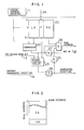
- a logical address which is given when the access to the main storage is requested is set in a logical address register 21.
- a predetermined logical operation namely, hashing
- nine bits of the logical address bits of the logical address register 21 are used to access the TLB 20, that is, to read out an entry thereof.
- a comparator 22 compares a logical address read out from the TLB 20 with upper bits of the register 21 other than the bits used for accessing the TLB 20, and outputs a logical value "1" when the upper bits of the register 21 coincide with the read-out logical address.
- the output of the comparator 22 is applied to an access control circuit 23, together with an F bit which is read out from an entry of the TLB 20 where the above real address exists.
- the access control circuit 23 is further supplied with an HA access mode bit from a signal line 13. The bit from the signal line 13 takes a value "1" when the data processing system is operated in the HA access mode, and takes a value "0" when the access mode of the system is not the HA access mode.
- the output of the access control circuit 23 is applied to an OR circuit 24, together with a signal which is supplied by a signal line 14 and indicates another addressing-exception generated in the data processing system.
- the OR circuit 24 delivers an output having the level "1", that is, an addressing-exception signal.
- the output of the OR circuit 24 is also applied to an AND circuit 26 through an inverter 25.
- the AND circuit 26 is closed, and therefore prevents the real address read out of the TLB 20 from being transferred to the main storage.
- an address of the main storage which is to be accessed is set in a register 10.
- a boundary address for partitioning the main storage into the HA and SA is previously set in a register 11.
- a comparator 12 compares the contents of the register 10 with those of the register 11, and delivers an output having the level "1" or "0" depending upon whether the to-be-accessed address of the main storage is greater or not greater in address number than the boundary address, respectively.
- the potential of the singal line 13 is kept at the level "1" when a data processing system is operated in the HA access mode, and is kept at the level "0" when the access mode of the system is not the HA access mode.
Landscapes
- Engineering & Computer Science (AREA)
- Theoretical Computer Science (AREA)
- Computer Security & Cryptography (AREA)
- Physics & Mathematics (AREA)
- General Engineering & Computer Science (AREA)
- General Physics & Mathematics (AREA)
- Memory System Of A Hierarchy Structure (AREA)
- Storage Device Security (AREA)
Claims (5)
- Ein Zugriffsteuersystem für einen Speicher, das für die Verwendung in einem Datenverarbeitungssystem ausgebildet ist, in dem ein Speicher in einen Hardwarebereich (HA), auf den normale Programme nicht zugreifen können, und in einen Softwarebereich (SA) zum Speichern der normalen Programme unterteilt ist und in dem der Zugriff auf den Speicher entsprechend einer auf den Speicher zugreifenden Adresse und entsprechend einem Zugriffbetriebsart-Signal (13), das angibt, ob auf den Hardwarebereich (HA) zugegriffen werden kann oder nicht, gesteuert wird, wobei das Zugriffsteuersystem eine Adressenregistereinrichtung (20) mit einer Mehrzahl von Eintragungen aufweist, um die Inhalte einer Eintragung auszulesen, die einer Adresse entspricht, bei der auf den Speicher zugegriffen werden soll, wobei jede der Eintragungen eine Adresse des Speichers enthält,
und wobei das Zugriffsteuersystem eine Komparatoreinrichtung (22) enthält, um auf der Grundlage der ausgegebenen Inhalte der Eintragung ein Signal auszugeben, das angibt, ob die Zugriffszieladresse des Speichers in der Adressenregistereinrichtung (20) vorhanden ist,
dadurch gekennzeichnet, daß
jede Eintragung der Adressenregistereinrichtung (20) ein Zustandsbit (F) besitzt, das angibt, ob die Adresse im Hardwarebereich (HA) enthalten ist oder nicht;
und daß eine Zugriffsteuereinrichtung (23) vorgesehen ist, um den Zugriff auf den Speicher entsprechend dem Zugriffsbetriebsart-Signal (13), dem Zustandsbit (F) und dem Signal von der Komparatoreinrichtung (22) zu steuern. - Ein Zugriffsteuersystem gemäß Anspruch 1, in dem das Datenverarbeitungssystem ein Adressenübersetzungsverfahren verwendet, in dem eine logische Adresse (LA) in eine reale Adresse (RA) übersetzt werden, um auf den Speicher zuzugreifen, und in dem die Adressenregistereinrichtung (20) in jeder Eintragung ein Paar aus einer logischen und einer realen Adresse (LA, RA) hält, wobei das Zugriffsteuersystem ferner eine Ausgabeeinrichtung (26) umfaßt, um die an den Speicher gerichtete Übertragung der realen Adresse, die aus der Adressenregistereinrichtung (20) entsprechend dem Zustandsbit (F), dem Zugriffsbetriebsart-Signal (13) und einem im Datenverarbeitungssystem erzeugten Ausnahme-Adressierungssignal ausgelesen wird, freizugeben/zu sperren.
- Ein Zugriffsteuersystem gemäß Anspruch 2, in dem die Zugriffsteuereinrichtung (23) ein Signal ausgibt, das angibt, daß auf den Hardwarebereich (HA) nicht zugegriffen werden muß, wenn das Zugriffsbetriebsart-Signal (13) eine Zugriffsbetriebsart angibt, das einen Zugriff auf den Hardwarebereich (HA) nicht erlaubt, in dem das Signal von der Komparatoreinrichtung (22) angibt, daß die Zugriffszieladresse in der Adressenregistereinrichtung (20) vorhanden ist und in dem das Zustandsbit (F) angibt, daß die Zugriffszieladresse des Speichers gleichzeitig im Hardwarebereich (HA) enthalten ist.
- Ein Zugriffsteuersystem gemäß einem der Ansprüche 1 bis 3, das ferner eine Registereinrichtung (11) umfaßt, die die Adressen an der Grenze zwischen dem Hardwarebereich und dem Softwarebereich hält.
- Ein Zugriffsteuersystem gemäß einem der Ansprüche 1 bis 4, dadurch gekennzeichnet, daß es ferner umfaßt:
eine Einrichtung (12), die arbeitet, wenn die Zugriffszieladresse des Speichers nicht in der Adressenregistereinrichtung (20) vorhanden ist und die auf die Registereinrichtung (11) Bezug nimmt, um festzustellen, ob die reale Adresse (RA) im Hardwarebereich (HA) enthalten ist oder nicht, und die das Zustandsbit (F) entsprechend dem Ergebnis der Feststellung erzeugt; und eine Einrichtung (28) zum Eintragen des erzeugten Zustandsbits (F) in eine Eintragung der Adressenregistereinrichtung (20), wenn die logische (LA) und die reale Adresse (RA) in die Adressenregistereinrichtung (20) eingetragen ist.
Applications Claiming Priority (2)
| Application Number | Priority Date | Filing Date | Title |
|---|---|---|---|
| JP215555/83 | 1983-11-16 | ||
| JP58215555A JPS60107156A (ja) | 1983-11-16 | 1983-11-16 | デ−タ処理システム |
Publications (3)
| Publication Number | Publication Date |
|---|---|
| EP0142819A2 EP0142819A2 (de) | 1985-05-29 |
| EP0142819A3 EP0142819A3 (en) | 1988-07-27 |
| EP0142819B1 true EP0142819B1 (de) | 1992-05-20 |
Family
ID=16674364
Family Applications (1)
| Application Number | Title | Priority Date | Filing Date |
|---|---|---|---|
| EP84113746A Expired EP0142819B1 (de) | 1983-11-16 | 1984-11-14 | Zugriffsteuerungsanordnung für einen Speicher mit Hardware- und Softwarebereichen |
Country Status (4)
| Country | Link |
|---|---|
| US (1) | US4710894A (de) |
| EP (1) | EP0142819B1 (de) |
| JP (1) | JPS60107156A (de) |
| DE (1) | DE3485737D1 (de) |
Families Citing this family (9)
| Publication number | Priority date | Publication date | Assignee | Title |
|---|---|---|---|---|
| US4774653A (en) * | 1985-08-07 | 1988-09-27 | Hewlett-Packard Company | Hybrid hardware/software method and apparatus for virtual memory address translation using primary and secondary translation buffers |
| JPS62174851A (ja) * | 1986-01-29 | 1987-07-31 | Hitachi Ltd | バツフア記述制御方式 |
| JP2635310B2 (ja) * | 1986-03-04 | 1997-07-30 | 松下電器産業株式会社 | アドレス変換装置 |
| JPH0752405B2 (ja) * | 1988-12-14 | 1995-06-05 | 日本電気株式会社 | シングルチップマイクロコンピュータ |
| JPH07113898B2 (ja) * | 1989-05-09 | 1995-12-06 | 株式会社日立製作所 | 障害検出方式 |
| JPH0467243A (ja) * | 1990-07-06 | 1992-03-03 | Mitsubishi Electric Corp | データ処理装置 |
| JPH055143U (ja) * | 1991-06-29 | 1993-01-26 | 株式会社田窪工業所 | 香気発散器 |
| US5475829A (en) * | 1993-03-22 | 1995-12-12 | Compaq Computer Corp. | Computer system which overrides write protection status during execution in system management mode |
| JPH08161185A (ja) * | 1994-12-02 | 1996-06-21 | Hitachi Ltd | 仮想計算機システムのゲスト実行制御方式 |
Family Cites Families (11)
| Publication number | Priority date | Publication date | Assignee | Title |
|---|---|---|---|---|
| JPS5540950B2 (de) * | 1974-11-30 | 1980-10-21 | ||
| US4173783A (en) * | 1975-06-30 | 1979-11-06 | Honeywell Information Systems, Inc. | Method of accessing paged memory by an input-output unit |
| JPS52123834A (en) * | 1976-04-09 | 1977-10-18 | Fujitsu Ltd | Processing of memory and key information |
| US4038645A (en) * | 1976-04-30 | 1977-07-26 | International Business Machines Corporation | Non-translatable storage protection control system |
| US4093987A (en) * | 1977-03-24 | 1978-06-06 | International Business Machines Corporation | Hardware control storage area protection method and means |
| US4373179A (en) * | 1978-06-26 | 1983-02-08 | Fujitsu Limited | Dynamic address translation system |
| US4500952A (en) * | 1980-05-23 | 1985-02-19 | International Business Machines Corporation | Mechanism for control of address translation by a program using a plurality of translation tables |
| US4456954A (en) * | 1981-06-15 | 1984-06-26 | International Business Machines Corporation | Virtual machine system with guest architecture emulation using hardware TLB's for plural level address translations |
| US4451884A (en) * | 1982-02-02 | 1984-05-29 | International Business Machines Corporation | Cycle stealing I/O controller with programmable offline mode of operation |
| US4472790A (en) * | 1982-02-05 | 1984-09-18 | International Business Machines Corporation | Storage fetch protect override controls |
| US4573119A (en) * | 1983-07-11 | 1986-02-25 | Westheimer Thomas O | Computer software protection system |
-
1983
- 1983-11-16 JP JP58215555A patent/JPS60107156A/ja active Pending
-
1984
- 1984-11-14 DE DE8484113746T patent/DE3485737D1/de not_active Expired - Lifetime
- 1984-11-14 EP EP84113746A patent/EP0142819B1/de not_active Expired
- 1984-11-15 US US06/671,618 patent/US4710894A/en not_active Expired - Lifetime
Also Published As
| Publication number | Publication date |
|---|---|
| EP0142819A2 (de) | 1985-05-29 |
| JPS60107156A (ja) | 1985-06-12 |
| DE3485737D1 (de) | 1992-06-25 |
| US4710894A (en) | 1987-12-01 |
| EP0142819A3 (en) | 1988-07-27 |
Similar Documents
| Publication | Publication Date | Title |
|---|---|---|
| US5257361A (en) | Method and apparatus for controlling one or more hierarchical memories using a virtual storage scheme and physical to virtual address translation | |
| US5023777A (en) | Information processing system using domain table address extension for address translation without software modification | |
| US4985828A (en) | Method and apparatus for generating a real address multiple virtual address spaces of a storage | |
| CA1226372A (en) | Address translation control system | |
| US5930833A (en) | Logical cache memory storing logical and physical address information for resolving synonym problems | |
| US5182805A (en) | Method and system for determining copy-on-write condition | |
| US4996641A (en) | Diagnostic mode for a cache | |
| US4483003A (en) | Fast parity checking in cache tag memory | |
| EP0316252B1 (de) | Speicheraddressierungsfehlererkennung | |
| JPS6134178B2 (de) | ||
| US4710894A (en) | Access control system for storage having hardware area and software area | |
| US4658356A (en) | Control system for updating a change bit | |
| US5276829A (en) | Data processing system including cache memory for rapidly converting a logical address into a physical address using shared memory flag | |
| EP0425771A2 (de) | Wirksamer Mechanismus zur Versorgung feinkörniger Speicherschutzbereiche | |
| US6374334B1 (en) | Data processing apparatus with a cache controlling device | |
| US4424564A (en) | Data processing system providing dual storage of reference bits | |
| JPH02254553A (ja) | 情報処理装置 | |
| US6889308B1 (en) | Method and apparatus for protecting page translations | |
| JP3030037B2 (ja) | 主記憶装置 | |
| JPS6250863B2 (de) | ||
| JP3047839B2 (ja) | シングルチップ・マイクロコンピュータ | |
| JPH0210448A (ja) | キャッシュメモリシステム | |
| JPS626351A (ja) | 記憶保護装置 | |
| JPH0256039A (ja) | 記憶保護制御方式 | |
| JPH0337217B2 (de) |
Legal Events
| Date | Code | Title | Description |
|---|---|---|---|
| PUAI | Public reference made under article 153(3) epc to a published international application that has entered the european phase |
Free format text: ORIGINAL CODE: 0009012 |
|
| AK | Designated contracting states |
Designated state(s): DE FR GB |
|
| PUAL | Search report despatched |
Free format text: ORIGINAL CODE: 0009013 |
|
| AK | Designated contracting states |
Kind code of ref document: A3 Designated state(s): DE FR GB |
|
| 17P | Request for examination filed |
Effective date: 19880728 |
|
| 17Q | First examination report despatched |
Effective date: 19900508 |
|
| GRAA | (expected) grant |
Free format text: ORIGINAL CODE: 0009210 |
|
| AK | Designated contracting states |
Kind code of ref document: B1 Designated state(s): DE FR GB |
|
| REF | Corresponds to: |
Ref document number: 3485737 Country of ref document: DE Date of ref document: 19920625 |
|
| ET | Fr: translation filed | ||
| PLBE | No opposition filed within time limit |
Free format text: ORIGINAL CODE: 0009261 |
|
| STAA | Information on the status of an ep patent application or granted ep patent |
Free format text: STATUS: NO OPPOSITION FILED WITHIN TIME LIMIT |
|
| 26N | No opposition filed | ||
| PGFP | Annual fee paid to national office [announced via postgrant information from national office to epo] |
Ref country code: FR Payment date: 20010919 Year of fee payment: 18 |
|
| PGFP | Annual fee paid to national office [announced via postgrant information from national office to epo] |
Ref country code: GB Payment date: 20011102 Year of fee payment: 18 |
|
| REG | Reference to a national code |
Ref country code: GB Ref legal event code: IF02 |
|
| PGFP | Annual fee paid to national office [announced via postgrant information from national office to epo] |
Ref country code: DE Payment date: 20020130 Year of fee payment: 18 |
|
| PG25 | Lapsed in a contracting state [announced via postgrant information from national office to epo] |
Ref country code: GB Free format text: LAPSE BECAUSE OF NON-PAYMENT OF DUE FEES Effective date: 20021114 |
|
| PG25 | Lapsed in a contracting state [announced via postgrant information from national office to epo] |
Ref country code: DE Free format text: LAPSE BECAUSE OF NON-PAYMENT OF DUE FEES Effective date: 20030603 |
|
| GBPC | Gb: european patent ceased through non-payment of renewal fee | ||
| PG25 | Lapsed in a contracting state [announced via postgrant information from national office to epo] |
Ref country code: FR Free format text: LAPSE BECAUSE OF NON-PAYMENT OF DUE FEES Effective date: 20030731 |
|
| REG | Reference to a national code |
Ref country code: FR Ref legal event code: ST |