EP0144245A2 - Sender- und Empfängersystem - Google Patents
Sender- und Empfängersystem Download PDFInfo
- Publication number
- EP0144245A2 EP0144245A2 EP84308481A EP84308481A EP0144245A2 EP 0144245 A2 EP0144245 A2 EP 0144245A2 EP 84308481 A EP84308481 A EP 84308481A EP 84308481 A EP84308481 A EP 84308481A EP 0144245 A2 EP0144245 A2 EP 0144245A2
- Authority
- EP
- European Patent Office
- Prior art keywords
- frequency
- signal
- analyzer
- transmitter
- reference frequency
- Prior art date
- Legal status (The legal status is an assumption and is not a legal conclusion. Google has not performed a legal analysis and makes no representation as to the accuracy of the status listed.)
- Withdrawn
Links
Images


Classifications
-
- H—ELECTRICITY
- H04—ELECTRIC COMMUNICATION TECHNIQUE
- H04L—TRANSMISSION OF DIGITAL INFORMATION, e.g. TELEGRAPHIC COMMUNICATION
- H04L27/00—Modulated-carrier systems
- H04L27/26—Systems using multi-frequency codes
Definitions
- the present invention relates to a transmitter/ receiver system for data communications.
- Transmitter/receiver systems employing a multi-frequency signal have heretofor employed a method of frequency-modulating a carrier with the multi-frequency signal for transmission.
- This method is advantageous in that any frequency drift of the carrier due for example to temperature does not affect the frequency of the multi-frequency signal.
- the method has the following two drawbacks:
- a transmitter/ receiver system comprising a transmitter having a multi-frequency signal generator for issuing a signal of a reference frequency and then a signal composed of a frequency sequence having information indicative of frequency differences with the reference frequency, and a receiver having a frequency analyzer for analyzing the frequencies of the signal from the transmitter and an information decoder supplied with a signal from the frequency analyzer for decoding the information based on the frequency difference between the signal of the frequency sequence and the signal of the reference frequency.
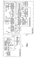
- FIG. 1 shows in block form a transmitter/receiver system according to an embodiment of the present invention.
- the transmitter/receiver system is generally composed of a transmitter A and a receiver B.
- the transmitter A has an input circuit 1 and a multi-frequency signal generator 7.
- the multi-frquency signal generator 7 comprises a D/A converter 2, a high-frequency oscillator circuit 4, and a variable-capacity diode 3.
- the transmitter 6 also has a transmission circuit 5 and a
- the receiver B has a reception antenna 8, a high-frequency amplifier 9, a local oscillator 11, a frequency converter 10, an intermediate-frequency amplifier 12, a local oscillator 14, a frequency converter 13, an A/D converter 15, a frequency analyzer 16, an information decoder 17, an analyzed frequency control cicuit 18, comparator 20, and a recorrecting circuit 19.
- the frequency analyzer 16, the information decoder 17, the analyzed frequency control circuit 18, the comparator 20, and the recorrecting circuit 19 are constructed in the form of a microcomputer 22.
- the receiver B also includes an output circuit 21.
- Operation of the transmitter/receiver system is as follows: Digital information from the input circuit 1 is applied to the A/ D converter 2 in the multi-frequency signal generator 7, and converted thereby into an analog quantity, which controls the capacitance of the variable-capacity diode 3 to control a high frequency produced by the high-frequency oscillator 4.
- Digital information from the input circuit 1 is applied to the A/ D converter 2 in the multi-frequency signal generator 7, and converted thereby into an analog quantity, which controls the capacitance of the variable-capacity diode 3 to control a high frequency produced by the high-frequency oscillator 4.
- a digital signal having a reference frequency f 0 is issued from the input circuit 1 and then a digital signal representative of input information is issued therefrom .
- the digital signal of the input information is converted by the D/A converter 2 into analog quantity, which varies the high frequency of the high-frequency oscillator 4 dependent on the information.
- FIG. 2(a) is a spectrum diagram of freuqencies that can be generated by the multi-frequency generator 7.
- FIGS. 2(b) through 2(e) are illustrative of frequencies issued from the multi-frequency generator 7.
- the multi-frequency generator 7 is basically differennt in function from conventional multi-frequency generators in that it has a reference frequency f 0 and information is defined in relation to the reference frequency f 0 .
- the following table shows an example in which pieces of information are defined as differences with the reference frequency.
- FIG. 2(b) illustrates one example of the output from the multi-frequency generator 7.
- the reference"frequency f0 is generated, and then a series of frequencies containing the information are generated.
- the pieces of information are issued in a succession of numeral 3, numeral 8, numeral 9, and numeral 4 in the order named.
- the signal of FIG. 2(b) is amplified by the transmitter 5, and transmitted as an electromagnetic wave by the transmission antenna 6.
- the receiver B will now be described.
- the reception antenna 8 through the intermediate-frequency amplifier 12 operate in the same manner as that of the corresponding parts in a conventional superheterodyne receiver.
- An output signal from the intermediate-frequency amplifier 12 is converted by the frequency converter 13 into a signal of a lower frequency.
- the frequency converter 13 converts the the signal into a frequency band which can easily be processed by the frequency analyzer 16.
- the converted frequency can be varied as desired in the frequency converter 13.
- the output from the frequency converter 13 has a spectrum which is shifted in parallel from the spectrum of FIG. 2(a) on a frequency basis, with no variation in freuqency differences between the spectra.
- the output signal from the frequency converter 13 is converted by an A/D converter 15 into a digital signal, which is then processed by the microcomputer 22.
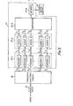
- FIG. 3 is a block diagram of the frequency analyzer 16.
- the frequency analyzer 16 is composed of eleven filter groups 16-1 through 16-11 for separting the signal from the frequency converter 13 into respective spectra, each filter group being composed of a plurality of filters.
- the filter group 16-1 comprises filters 101, 102, 102
- the filter group 16-2 comprises filters 104, 105, 106.
- the frequency of FIG. 2(b) is applied, as freuqency- shifted, to the frequency analyzer 16, in which a signal of a frequency corresponding to the reference-frequency signal f 0 is first issued from one of the filter groups and applied to the information decoder 17.
- the information decoder 17 recognizes the first signal as the reference-frequency signal f 0 .
- the filter groups 16-5, 16-6 are arranged as shown in FIG. 4(a).
- the filter group 16-6 serves to detect a signal in the vicinity of the center of the intermediate-frequency amplifier 12. In case the transmitted frequency and the local oscillation frequency of the receiver are properly adjusted, the reference frequency f 0 is detected at the position of the central filter 117 of the filter group 16-6.
- the reference frequency f 0 is detected at the position f 01 in FIG. 4(b) due to a variation in the local oscillation frequency.
- the filter 113 in the filter group 16-5 issues an output signal.
- the local oscillator 11 is controlled to correct the local oscillation frequency so that the reference frequency f o will be shifted from the position f 01 to the position f 02 in FIG. 4(b).
- a voltage-variable . capacitance element for example, is employed as a control element for controlling the local oscillation frequency, and the information decoder circuit 17 generates eleven control voltages.
- the central control voltage among the eleven control voltages is applied to the voltage-variable capacitance element.
- the difference 1 with the filter group 16-6 is computed, and the control voltage for the voltage-variable capacitance element is varied one step to thereby shift the reference freuqency f O from f 01 to f 02 .
- the filters constituting the filter groups 16-1 through 16-6 are divided into different groups as shown in FIG. 4(c) so that the position of f 02 of FIG . 4(b) will be brought to the centger of the filter group 16-6.
- the filter group 16-5 is composed of filters-112, 113, 114, and the filter group 16-6 is composed of filters 115, 116, 117.
- the filter grouping as shown in FIG. 4(c) is carried out by the analyzed frequency control circuit 18 which is responsive to the result of the arithmetic operation in the information decoder 17 for applying a control signal to the frequency analyzer 16.
- the comparator 20 ascertains whether the signal of the reference frequency is actually issued from the central fitler of the filter group located in the vicinity of the center of the band of the intermediate-frequency amplifier 12. If the reference frequency f 0 is confirmed, then the subsequent signal is received.
- the frequency analyzer 16 is recorrected by the recorrecting circuit 19 for correcting control linearity when a signal is obtained in the vicinity of the reference frequency f oe
- the information decoder 17 derives information from the relationship with respect to the reference frequency f o , or from the frequency difference determined by the above table, for example, and drives the output circuit 21.
- the frequency f -1 indicative of the difference between the reference freuqency f 0 and - ⁇ f as shown in FIG. 4(d) is applied to the frequency analyzer 16.
- the circuit is designed such that if the reference frequency f 0 is located at the lefthand end of the band of the central filter 116 of the filter group 16-6, then the frequency f -1 applied next will be brought to the lefthand end of the band of the central filter l13 of the filter group 16-5. If the filter bandwidth and the central frequency of the filters are varied slightly due to temperature changes, then f' -1 would be located at the righthand end of the band of the filter 112 of the filter group 16-5 as shown in FIG. 4(d). However, a plurality of filters are grouped and one frequency is assigned thereto, as shown in FIG. 4(c), the filter group 16-5 with the frequency difference - ⁇ f is selected and no error is caused in signal discrimination.
- each filter group in FIG. 3 is composed of three filters, each filter may be of a narrower bandwidth and each filter group may comprise more filters, so that the S/N ratio will be more improved, information can be decoded at a lower level, and the distance for which signals can be transmitted can be increased.
- the difference with the reference frequency f 0 is transmitted as information, and the local oscillator 11 and the frequency analyzer 16 are controlled so that the reference frequency f 0 will be positioned in the center of the band of the intermediate-freuqency amplifier 12. Therefore, there is no possibility for the failure of receiving information due to variations in the local frequency, and the reference frequency f 0 is prevented from being discriminated in error due to noise. It is not necessary to increase the signal receiving. bandwidth to provide against temperature changes.
- the receiver may be of a narrow bandwidth to improve the S/N ratio to a large extent and increase the distance for which signals can be transmitted. Since the comparator 20 supervises the reference frequency, the reference frequency is prevented from being discriminated in error due to noise.
- the control linearity can be controlled by the recorrecting circuit 19, the control linearity of the local oscillator 11 and the frequency analyzer 16 may not be strictly ensured.
- FIG. 2(c) is illustrative of a signal transmission form in which the reference frequency f O is inserted between information frequencies.
- FIG. 2(d) shows a signal transmission form in which after a frequency f -n shifted from the reference frequency f O by - nf has been transmitted, a signal of f n of an inverted sign shifted the distance n ⁇ f is transmitted.
- two reference frequencies f l , f -1 are employed.
- the signal form subsequent to the reference frequencies f 1 , f -1 is the same as shown in FIG. 2(c). Furthermore, the signal form is not limited to those shown in FIGS. 2(b) through 2(e), but may be any form provided that the reference frequency is first transmitted, and thereafter a signal containing information is transmitted. For example, signals of several frequencies may be transmitted on a parallel basis, or the reference frequency may be transmitted again at a final end to indicate the ending of communication.
- the controll local oscillator may be either the circuit 11 or the circuit 14.
- the frequency analyzer 16 may comprise an analog filter or a circuit utizizing a Fourier transform process.
- the informatin decoder 17 also can supply the output circuit 21 with a signal indicative of the ratio of the greatest amount of energy of a frequency component to the amount of energy of other frequency components.
- the output circuit 21 energizes a level meter of an LED array dependent on the energy amount ratio. This arrangement can be used as an electric-field-strength discriminating device for indicating the level of the signal picked up by the reception antenna 8.
- the informaiton decoder 17 will be described in more detail with reference to FIG. 5.
- the information decoder 17 includes a memory group 17-1 composed of n memories 1 through n, an adder group 17-2 composed of n adders 1 through n, an comparator 17-3, and a memory 17-4.
- the information decoder 17 is connected to the output circuit 21. Functionally identical parts are denoted by identical reference characters in FIG. 1.
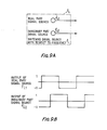
- FIG. 6(a) A signal A applied to an input terminal is shown in FIG. 6(a).
- the signal A is converted by the A/D converter 15 into a digital signal which is analyzed as to frequency by the frequency analyzer 16.
- the frequency analyzer 16 introduces data for a T/4 second and effects a Fourier transform for frequency analysis.
- FIG. 6(b) shows the manner in which the frequency is analyzed by the frequency analyzer 16.
- Each of time intervals T 1 through T15 is a T/4 second serving as a time period for introducing data for Fourier transform.
- the frequency analyzer 16 then issues analyzed outputs as indicated by K i through K 14 .
- FI G A signal A applied to an input terminal is shown in FIG. 6(a).
- the signal A is converted by the A/D converter 15 into a digital signal which is analyzed as to frequency by the frequency analyzer 16.
- the frequency analyzer 16 introduces data for a T/4 second and effects a Fourier transform for frequency analysis.
- FIG. 6(b) shows the
- FIGS. 7(a) through (d) show analyzed outputs K 2 through K 4 .
- the S/N ratio of the signal A applied to the input terminal is poor, that is, noise is included in the signal A.
- the analyzed outputs R 1 through K 4 include noise-dependent signal components other than the desired signal f
- FIG. 7(b) shows an example in which a noise component fn is greater in level than the desired signal f 2 .
- the frequency analyzer 16 issues digital signals proportional to the magnitudes of frequency components as outputs f 1 through fn, and the data are stored in the memories 1 through n.
- the signal K 2 indicative of the anaylized result in T2 is stored in the memories 1 through n.
- the adders 1 through n add the four data k 1 , K 2 , K 3 , K4 stored respectively in the memories 1 through n. More specifically, the adder 1 adds frequency components f 1 of the signals R 1 , R 2 , R 3 , R 4 , and the adder 2 adds frequency components f 2 of the signals R 1 , K 2' R 3 , K 4 .
- the adder group 17-2 issues signals indicative of the added four data K 1 , K 2 , K 3 , K 4 as outputs f 1 through fn for the respective frequency components.
- the frequency components generated due to noise are averaged in time and the signal component f 2 has its level much higher than the noise components.
- the output of FIG. 7(e) from the adder group is applied to the comparator 17-3 in which the frequency components are compared.
- the frequency component f 2 of the greatest energy is issued from the comparator 17-3 to the memory 17-4.
- a next freuqency analysis is effected by the frequency analyzer 16, which generates a signal K 5 .
- the memory group 17-1 dischards the oldest data K 1 and newly stores the data K 5 . Therefore, the memory group 17-1 stores the data K 2 , K3 , K4 , KS .
- the adder group 17-2 adds the above four data, and the sum is applied to the comparator 17-3 in which the levels of frequency components are compared, and then the frequency component of the greatest energy is stored in the memory 17-4. Subsequently, four data are added by the adder group 17-2 each time a frequency analysis is carried out by the frequency analyzer 16, frequency components of the greatest energy are detected by the comparator 17-3, and successively stored in the memory 17-4.
- FIG. 6(c) shows the manner in which the data are stored in the memory 17-4.
- data of the greatest energy among the same frequency components that is, added data in the time coinciding with the repetitive period of the signal
- data a, b, c in FIG. 6(c) are picked up and applied to the output circuit 21 to drive the same.
- the memory 17-4 may be of any memory provided it can store a signal from the comparator 17-3, compare the stored signal with a next signal applied, and determine whether the signal is to be applied to the output circuit 21.
- the frequency analyzer has an input terminal 201, a switching signal source 202, a sign switching unit 203, an adder 204, and an output terminal 205.
- the frequency analyzer thus constructed will operate as follows: :
- a frequency analyzer 16 will be described with reference to FIG. 11.
- the frequency analyzer 16 of FIG. 11 employes a microcomputer operating on the basis of a high-speed Fourier transform algorithm.
- the frequency analyzer comprises an input terminal 201, an A/D converter 15, a data bus 206, a microcomputer 207, a memory 208, an output device 209.
- a signal to be analyzed as to frequency is supplied through the input terminal 201, and converted into a digital quantity by the A/D converter 15.
- the digital signal is then stored into the memory 208 through the data bus 206 under the control of the microcomputer 207.
- the present invention is characterized in that W N is given as U N which is defined as follows: Therefore, an equation for transforming the input signal sequence x(n) into a sequence X(k) in the frequency domain according to the invention is given by: The value of U nK N is selected dependent on whether the real and imaginary parts are positive or negative after W nK N has been computed. Re(W N ) and Im(W N ) are indicative respectively of the real and imaginary parts of W N .
- the decimation-in-time algorithm of a high-speed Fourier transform is based on breaking up the input signal sequence x(n) sequentially into smaller subsequences.
- the signal sequence x(n) is supplied through the input terminals 210 and subjected to frequency analyses at N/2 points in an N/2-point frequency analyzer 211 which issues G(k), H(k).
- FIG. 12(b) is illustrative of a flow-graph in which the N/2- point frequency analyzer 211 is further dividedinto 2- point frequency analyzers 212.
- branches joined at nodal points represent addition.
- FIG. 13 is illustrative of branches having coefficients.
- FIG. 13(a) shows one matrix of the flow-graphs of FIG. 12.
- FIG. 13(b) shows the matrix which is accomplished by a switching signal source 202 and a sign switching unit 203.
- the basic computation in this flow graph is represented by one X-shaped matrix from the mth step to the (m + l)th step, as shown in FIG. 15 (a).
- the computation is given by: Since is also - 1, and the above equations become: This is illustrated in FIG. 15(b). In this manner, the number of additions is reduced to (N/2)log 2 N.
- the frequency analysis can be performed without using multiplication.
- a decimation-in-frequency algorithm may also be used in which the input signal sequence first remains unchanged and is rearranged after a frequency analysis has been effected. The requirement is that the frequency analysis is effected without using multiplication by controlling the signs of the input signals.
Landscapes
- Engineering & Computer Science (AREA)
- Computer Networks & Wireless Communication (AREA)
- Signal Processing (AREA)
- Reduction Or Emphasis Of Bandwidth Of Signals (AREA)
- Digital Transmission Methods That Use Modulated Carrier Waves (AREA)
- Transmitters (AREA)
Applications Claiming Priority (8)
| Application Number | Priority Date | Filing Date | Title |
|---|---|---|---|
| JP58230807A JPS60123140A (ja) | 1983-12-07 | 1983-12-07 | 受信装置 |
| JP230807/83 | 1983-12-07 | ||
| JP59085422A JPS60229450A (ja) | 1984-04-26 | 1984-04-26 | 情報解読装置 |
| JP85422/84 | 1984-04-26 | ||
| JP59102920A JPH0642688B2 (ja) | 1984-05-22 | 1984-05-22 | 受信装置 |
| JP102920/84 | 1984-05-22 | ||
| JP129816/84 | 1984-06-22 | ||
| JP59129816A JPS617898A (ja) | 1984-06-22 | 1984-06-22 | 周波数分析装置 |
Publications (2)
| Publication Number | Publication Date |
|---|---|
| EP0144245A2 true EP0144245A2 (de) | 1985-06-12 |
| EP0144245A3 EP0144245A3 (de) | 1987-09-30 |
Family
ID=27467107
Family Applications (1)
| Application Number | Title | Priority Date | Filing Date |
|---|---|---|---|
| EP84308481A Withdrawn EP0144245A3 (de) | 1983-12-07 | 1984-12-06 | Sender- und Empfängersystem |
Country Status (2)
| Country | Link |
|---|---|
| US (1) | US4660215A (de) |
| EP (1) | EP0144245A3 (de) |
Cited By (7)
| Publication number | Priority date | Publication date | Assignee | Title |
|---|---|---|---|---|
| FR2607987A1 (fr) * | 1986-12-05 | 1988-06-10 | Thomson Csf | Procede et dispositif de modulation et de demodulation a plusieurs etats, a niveau de protection ajustable |
| GB2204466A (en) * | 1987-05-05 | 1988-11-09 | Kit Fun Ho | Frequency ratio transmission |
| RU2169993C1 (ru) * | 1999-12-23 | 2001-06-27 | Ишмухаметов Башир Гарифович | Приемник последовательных многочастотных сигналов |
| RU2207732C2 (ru) * | 2000-03-01 | 2003-06-27 | Сибирский государственный университет телекоммуникаций и информатики | Способ приема параллельного многочастотного составного сигнала и устройство для его осуществления |
| RU2226037C1 (ru) * | 2002-07-25 | 2004-03-20 | Федеральное Государственное унитарное предприятие Воронежский научно-исследовательский институт связи | Адаптивная система связи с повышенной помехозащищенностью |
| RU2249914C2 (ru) * | 2003-01-20 | 2005-04-10 | Федеральное государственное унитарное предприятие Омский научно-исследовательский институт приборостроения | Система связи |
| CN109217836A (zh) * | 2018-09-03 | 2019-01-15 | 南京邮电大学 | 四端口低反射式双工滤波器 |
Families Citing this family (12)
| Publication number | Priority date | Publication date | Assignee | Title |
|---|---|---|---|---|
| US4972435A (en) * | 1986-04-18 | 1990-11-20 | Ho Kit Fun | Frequency independent information transmission system |
| US4985895A (en) * | 1988-11-14 | 1991-01-15 | Wegener Communications, Inc. | Remote controlled receiving system apparatus and method |
| US5063574A (en) * | 1990-03-06 | 1991-11-05 | Moose Paul H | Multi-frequency differentially encoded digital communication for high data rate transmission through unequalized channels |
| US5136613A (en) * | 1990-09-28 | 1992-08-04 | Dumestre Iii Alex C | Spread Spectrum telemetry |
| US5341402A (en) * | 1991-02-19 | 1994-08-23 | Tokyo Electric Co., Ltd. | Automatic frequency control method and device for use in receiver |
| USRE37802E1 (en) | 1992-03-31 | 2002-07-23 | Wi-Lan Inc. | Multicode direct sequence spread spectrum |
| US5517433A (en) * | 1994-07-07 | 1996-05-14 | Remote Intelligence, Inc. | Parallel digital data communications |
| FR2736225B1 (fr) * | 1995-06-27 | 1997-08-01 | Gec Alsthom Transport Sa | Dispositif permettant de s'affranchir des problemes de diaphonie lors de la localisation d'un vehicule se deplacant le long de moyens de propagation d'ondes electromagnetiques |
| US6192068B1 (en) | 1996-10-03 | 2001-02-20 | Wi-Lan Inc. | Multicode spread spectrum communications system |
| US6424885B1 (en) * | 1999-04-07 | 2002-07-23 | Intuitive Surgical, Inc. | Camera referenced control in a minimally invasive surgical apparatus |
| US6505037B1 (en) * | 1999-06-29 | 2003-01-07 | Sharp Laboratories Of America, Inc. | Data unit detection including antenna diversity |
| RU2310992C2 (ru) * | 2005-05-30 | 2007-11-20 | Федеральное государственное унитарное предприятие Омский научно-исследовательский институт приборостроения | Радиоприемное устройство многочастотных сигналов |
Family Cites Families (8)
| Publication number | Priority date | Publication date | Assignee | Title |
|---|---|---|---|---|
| DE2029508A1 (de) * | 1970-06-15 | 1971-12-23 | Griebel Electronik | Einkanaliges System zur Übertragung von Informationsblöcken zu einem Rechner |
| JPS4951801A (de) * | 1972-09-20 | 1974-05-20 | ||
| US3866124A (en) * | 1973-06-21 | 1975-02-11 | Keith H Wycoff | Communication system incorporating signal delay |
| DE2441452C3 (de) * | 1973-08-31 | 1980-01-17 | Hitachi, Ltd., Tokio | Anordnung zur Ultraschall-Nachrichtenübertragung |
| US4291269A (en) * | 1979-06-28 | 1981-09-22 | Rca Corporation | System and method for frequency discrimination |
| US4306308A (en) * | 1979-09-14 | 1981-12-15 | Rca Corporation | Symbols communication system |
| EP0027152B1 (de) * | 1979-10-15 | 1990-08-22 | Alcatel Bell-Sdt S.A. | Verfahren und Vorrichtung zur Übertragung periodischer elektrischen Signale mit sehr geringer Frequenzfehlertoleranz |
| JPS59211357A (ja) * | 1983-05-16 | 1984-11-30 | Matsushita Electric Ind Co Ltd | 送受信装置 |
-
1984
- 1984-12-04 US US06/678,032 patent/US4660215A/en not_active Expired - Fee Related
- 1984-12-06 EP EP84308481A patent/EP0144245A3/de not_active Withdrawn
Cited By (11)
| Publication number | Priority date | Publication date | Assignee | Title |
|---|---|---|---|---|
| FR2607987A1 (fr) * | 1986-12-05 | 1988-06-10 | Thomson Csf | Procede et dispositif de modulation et de demodulation a plusieurs etats, a niveau de protection ajustable |
| EP0273815A1 (de) * | 1986-12-05 | 1988-07-06 | Thomson-Csf | Verfahren und Einrichtung mit einstellbarem Schutzniveau für Modulation und Demodulation mit verschiedenen Zuständen |
| US4905256A (en) * | 1986-12-05 | 1990-02-27 | Thomson Csf | Method and device for multistate modulation and demodulation with adjustable protection level |
| GB2204466A (en) * | 1987-05-05 | 1988-11-09 | Kit Fun Ho | Frequency ratio transmission |
| GB2204466B (en) * | 1987-05-05 | 1992-02-12 | Kit Fun Ho | Frequency independent information transmission system |
| RU2169993C1 (ru) * | 1999-12-23 | 2001-06-27 | Ишмухаметов Башир Гарифович | Приемник последовательных многочастотных сигналов |
| RU2207732C2 (ru) * | 2000-03-01 | 2003-06-27 | Сибирский государственный университет телекоммуникаций и информатики | Способ приема параллельного многочастотного составного сигнала и устройство для его осуществления |
| RU2226037C1 (ru) * | 2002-07-25 | 2004-03-20 | Федеральное Государственное унитарное предприятие Воронежский научно-исследовательский институт связи | Адаптивная система связи с повышенной помехозащищенностью |
| RU2249914C2 (ru) * | 2003-01-20 | 2005-04-10 | Федеральное государственное унитарное предприятие Омский научно-исследовательский институт приборостроения | Система связи |
| CN109217836A (zh) * | 2018-09-03 | 2019-01-15 | 南京邮电大学 | 四端口低反射式双工滤波器 |
| CN109217836B (zh) * | 2018-09-03 | 2022-05-31 | 南京邮电大学 | 四端口低反射式双工滤波器 |
Also Published As
| Publication number | Publication date |
|---|---|
| US4660215A (en) | 1987-04-21 |
| EP0144245A3 (de) | 1987-09-30 |
Similar Documents
| Publication | Publication Date | Title |
|---|---|---|
| EP0144245A2 (de) | Sender- und Empfängersystem | |
| CA1263717A (en) | Modulation detector and classifier | |
| CA1210118A (en) | Receivers for navigation satellite systems | |
| EP0296175B1 (de) | Verfahren und Anlage für digitale Uebertragung insbesondere zwischen und in Richtung bewegender Fahrzeuge | |
| Tuller | Theoretical limitations on the rate of transmission of information | |
| US20060143190A1 (en) | Handling of digital silence in audio fingerprinting | |
| JPH05508291A (ja) | 信号分類機を有する受信機 | |
| US6198781B1 (en) | Apparatus and method of demodulating coded signal under OFDM transmission | |
| US4723125A (en) | Device for calculating a discrete moving window transform and application thereof to a radar system | |
| EP1263181B1 (de) | Korrektur des Abtasttektaktes eines digitalen Demodulationssystems und Verfahren mittels Auswahl eines Polyfasenfilter | |
| US4845707A (en) | Frequency division multiplex/FM modulation recognition system | |
| US4698769A (en) | Supervisory audio tone detection in a radio channel | |
| JPS61296843A (ja) | コ−ド化デイジタル・デ−タ用信号対雑音比指数生成装置および方法 | |
| US4634966A (en) | Binary processing of sound spectrum | |
| US5263054A (en) | Method and system for interpolating baud rate timing recovery for asynchronous start stop protocol | |
| EP0053939A1 (de) | Fangschaltung für digitale, phasenverriegelte Schleife | |
| EP0358581A2 (de) | Anordnung zur Einzelworterkennung | |
| US4635217A (en) | Noise threshold estimator for multichannel signal processing | |
| US5220584A (en) | System for demodulation and synchronizing multiple tone waveforms | |
| US4344040A (en) | Method and apparatus for providing the in-phase and quadrature components of a bandpass signal | |
| US4577335A (en) | Coherent data communications technique | |
| US5862226A (en) | Automatic mode detection in digital audio receivers | |
| US20020067218A1 (en) | Circuit configuration for producing a quadrature-amplitude-modulated transmission signal | |
| US4348735A (en) | Cyclotomic tone detector and locator | |
| CN1134931C (zh) | 测量频差的方法和接收机 |
Legal Events
| Date | Code | Title | Description |
|---|---|---|---|
| PUAI | Public reference made under article 153(3) epc to a published international application that has entered the european phase |
Free format text: ORIGINAL CODE: 0009012 |
|
| AK | Designated contracting states |
Designated state(s): DE FR GB |
|
| PUAL | Search report despatched |
Free format text: ORIGINAL CODE: 0009013 |
|
| AK | Designated contracting states |
Kind code of ref document: A3 Designated state(s): DE FR GB |
|
| STAA | Information on the status of an ep patent application or granted ep patent |
Free format text: STATUS: THE APPLICATION IS DEEMED TO BE WITHDRAWN |
|
| 18D | Application deemed to be withdrawn |
Effective date: 19880331 |
|
| RIN1 | Information on inventor provided before grant (corrected) |
Inventor name: FUKUI, KIYOTAKE Inventor name: HORIIKE, YOSHIO Inventor name: NAGAISHI, YASUO |