EP0144593A1 - Steuersystem für einen Wechselrichter vom Spannungstyp - Google Patents
Steuersystem für einen Wechselrichter vom Spannungstyp Download PDFInfo
- Publication number
- EP0144593A1 EP0144593A1 EP84111725A EP84111725A EP0144593A1 EP 0144593 A1 EP0144593 A1 EP 0144593A1 EP 84111725 A EP84111725 A EP 84111725A EP 84111725 A EP84111725 A EP 84111725A EP 0144593 A1 EP0144593 A1 EP 0144593A1
- Authority
- EP
- European Patent Office
- Prior art keywords
- signal
- voltage
- pulse width
- width modulation
- inverter
- Prior art date
- Legal status (The legal status is an assumption and is not a legal conclusion. Google has not performed a legal analysis and makes no representation as to the accuracy of the status listed.)
- Granted
Links
- 238000001514 detection method Methods 0.000 claims abstract description 16
- 239000004065 semiconductor Substances 0.000 claims abstract description 4
- 238000010586 diagram Methods 0.000 description 6
- 230000006698 induction Effects 0.000 description 6
- 230000033228 biological regulation Effects 0.000 description 3
- 230000007935 neutral effect Effects 0.000 description 3
- 230000007306 turnover Effects 0.000 description 3
- 239000007787 solid Substances 0.000 description 2
- 230000003247 decreasing effect Effects 0.000 description 1
- 230000001934 delay Effects 0.000 description 1
- 230000004907 flux Effects 0.000 description 1
- 230000010354 integration Effects 0.000 description 1
- 238000000034 method Methods 0.000 description 1
- 230000001172 regenerating effect Effects 0.000 description 1
Images




Classifications
-
- H—ELECTRICITY
- H02—GENERATION; CONVERSION OR DISTRIBUTION OF ELECTRIC POWER
- H02M—APPARATUS FOR CONVERSION BETWEEN AC AND AC, BETWEEN AC AND DC, OR BETWEEN DC AND DC, AND FOR USE WITH MAINS OR SIMILAR POWER SUPPLY SYSTEMS; CONVERSION OF DC OR AC INPUT POWER INTO SURGE OUTPUT POWER; CONTROL OR REGULATION THEREOF
- H02M7/00—Conversion of AC power input into DC power output; Conversion of DC power input into AC power output
- H02M7/42—Conversion of DC power input into AC power output without possibility of reversal
- H02M7/44—Conversion of DC power input into AC power output without possibility of reversal by static converters
- H02M7/48—Conversion of DC power input into AC power output without possibility of reversal by static converters using discharge tubes with control electrode or semiconductor devices with control electrode
- H02M7/53—Conversion of DC power input into AC power output without possibility of reversal by static converters using discharge tubes with control electrode or semiconductor devices with control electrode using devices of a triode or transistor type requiring continuous application of a control signal
- H02M7/537—Conversion of DC power input into AC power output without possibility of reversal by static converters using discharge tubes with control electrode or semiconductor devices with control electrode using devices of a triode or transistor type requiring continuous application of a control signal using semiconductor devices only, e.g. single switched pulse inverters
- H02M7/5387—Conversion of DC power input into AC power output without possibility of reversal by static converters using discharge tubes with control electrode or semiconductor devices with control electrode using devices of a triode or transistor type requiring continuous application of a control signal using semiconductor devices only, e.g. single switched pulse inverters in a bridge configuration
- H02M7/53871—Conversion of DC power input into AC power output without possibility of reversal by static converters using discharge tubes with control electrode or semiconductor devices with control electrode using devices of a triode or transistor type requiring continuous application of a control signal using semiconductor devices only, e.g. single switched pulse inverters in a bridge configuration with automatic control of output voltage or current
- H02M7/53875—Conversion of DC power input into AC power output without possibility of reversal by static converters using discharge tubes with control electrode or semiconductor devices with control electrode using devices of a triode or transistor type requiring continuous application of a control signal using semiconductor devices only, e.g. single switched pulse inverters in a bridge configuration with automatic control of output voltage or current with analogue control of three-phase output
-
- H—ELECTRICITY
- H03—ELECTRONIC CIRCUITRY
- H03K—PULSE TECHNIQUE
- H03K7/00—Modulating pulses with a continuously-variable modulating signal
- H03K7/08—Duration or width modulation ; Duty cycle modulation
-
- H—ELECTRICITY
- H02—GENERATION; CONVERSION OR DISTRIBUTION OF ELECTRIC POWER
- H02M—APPARATUS FOR CONVERSION BETWEEN AC AND AC, BETWEEN AC AND DC, OR BETWEEN DC AND DC, AND FOR USE WITH MAINS OR SIMILAR POWER SUPPLY SYSTEMS; CONVERSION OF DC OR AC INPUT POWER INTO SURGE OUTPUT POWER; CONTROL OR REGULATION THEREOF
- H02M1/00—Details of apparatus for conversion
- H02M1/38—Means for preventing simultaneous conduction of switches
- H02M1/385—Means for preventing simultaneous conduction of switches with means for correcting output voltage deviations introduced by the dead time
Definitions
- the present invention relates to a control system for a voltage-type inverter comprising a bridge connection of electric valves each comprising a reverse parallel connection of a semiconductor switching element and a diode and converting a DC power to an AC power by means of pulse-width modulation control (hereinafter referred to as PWM control).
- PWM control pulse-width modulation control
- Fig. 1 shows a conventional system.
- a DC power from a DC power source 1 is converted to an AC power by an inverter bridge 2 and supplied to a load motor 3, which, for the purpose of description, will be assumed to be an induction motor.
- the inverter bridge 2 comprises a bridge connection of electric valves each comprising a reverse parallel connection of a transistor 21-26 and a diode 31-36.
- An inverter frequency setting device 4 provides a frequency reference voltage, which is applied to a ramp function generator 5, which limits the rate of change of the voltage.
- the output of the ramp function generator 5 is supplied to a voltage pattern generator 6, and an inverter output voltage pattern outputted by the voltage pattern generator 6 is supplied to an AC voltage reference circuit 8.
- the output of the ramp function generator 5 is converted, by a V/F converter (voltage-to-frequency converter) 7, to a frequency proportional to the inverter frequency.
- the AC voltage reference circuit 8 receives the voltage pattern output and the V/F converter output and produces voltage reference , , .
- An oscillator 9 generates a trigonal wave e t for modulation.
- Comparators 10, 11, 12 compare the trigonal wave e t with the voltage references , , , respectively to produce PWM ou puts PWM U , PWM V , PWM W , which are amplified by a drive circuit 13 and are used to drive the inverter bridge.
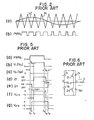
- P WM control is well. known, but, for an easier understanding of the invention, its fundamentals will be briefly discussed with reference to Fig. 2. Incidentally, today's control system often employs a microprocessor for the PWM operation, but the same principle is applied.
- phase U For the sake of simplicity, description is made with reference to one of the phases, e.g., phase U . Similar operations are performed with respect to other phases.
- the U-phase voltage reference V *U which is sinusoidal, is compared with the trigonal wave e t , and a PWM output PWM U is produced.
- the fundamental wave of the output PWM U is proportional to the voltage reference V *U .
- PWM control is accomplished by adjusting the magnitude and the frequency of the voltage reference V *U .
- Typical examples of the switching elements used in the inverter bridge are thyristors, transistors, gate- turn-off thyristors (GTO's). These elements have more or less delay in switching, particularly in turn-off. Also this delay time is not precisely known and can vary depending on various factors. For this reason, it is necessary to take a measure for ensuring that, at,no moment, the series connected switching element, such as the transistors 21 and 24 in Fig. 1 are concurrently conductive. As such a measure, a dead time is provided so that the transistor 24 is turned on certain time after the transistor 21 is turned off. Further description on this point is given with reference to Figs. 3 and 4.
- Fig. 3 shows, in detail, part of the drive circuit 13 of Fig. 1 which relates to one of the phases, i.e., phase U.
- the PWM signal PWM U is passed through an on-delay circuit 132 which delays, by a delay time T D , only the leading edge of the signal pulse.
- the output signal V 1 of the on-delay circuit 132 is amplified by a drive amplifier 134, whose output constitutes a drive signal V 21 for the transistor 21.
- the signal PWM U is also fed to a logic circuit 131, where it is inverted to become a signal PWM U , and is then passed through an on-delay circuit 133, similar to the circuit 132.
- the output signal V 2 of the on-delay circuit 133 is amplified by a drive amplifier 135, whose output constitutes a drive signal V 24 for the transistor 24.
- Fig. 4 shows the operation.
- the transistors 21, 24 are turned on and off by the signals V1, V 2 whose leading edges are lagging behind PWM U , PWM U , respectively, by T D .
- the turn-on time of the transistors 21, 24 is not more than 1 ⁇ sec. and can be neglected.
- the turn-off time toff of the transistors is several ⁇ sec to several tenths of ⁇ sec.
- the delay time T D is set to be two to three times the turn-off time. As a result, there is time interval when the transistors 21, 24 are both non-conductive, and during this time interval, the inverter output voltage is not definite. This point will be described with reference to Fig. 5.
- the inverter output voltage V U-O is a voltage of the inverter U-phase output with reference to a neutral point O which is an imaginary mid-point which results when the DC power source 1 is imaginarily divided into two parts 1a and 1 b .
- the inverter output line voltages can be derived, as is well known, from the differences between the voltages V U-O , V V-O , V W-O , i.e., the three output phase voltages on the respective output terminals with reference to the neutral point O.
- the voltage V U-O assumes a waveform shown in Fig. 5(g).- That is, while the transistors 21, 24 are both non-conductive, the load current I flows through the diode 31 into the DC power source 1 so that V U-O is positive during the period t 1 - t2 and the period t 4 - t 5 .
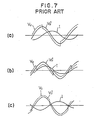
- the inverter output voltage in relation to the load current in a situation where the load motor is an induction motor.
- the voltage reference is indicated by a solid line while the actual inverter output voltage V U-O is indicated by a broken line.
- the load current is, as shown in Fig. 7(a), lagging by about 90°.
- the current is negative, so that the situation is like that of Fig. 5(g) and hence the actual inverter output voltage V U-O is higher (more positive) than the reference VU.
- the current is positive, so that the situation is like that of Fig. 5(f) and hence V U-O is lower (more negative) than .
- the inverter output voltage is generally increased as shown in Fig. 7(c).
- the inverter output voltage varies depending on the power factor of the load, or the phase of the current relative to the voltage.
- the amount of variation is substantially fixed regardless of the magnitude of the output voltage.
- the voltage regulation (change in the output voltage) is increased.
- the output voltage waveform is distorted (away from sinusoidal).
- magnetic flux of the induction motor is varied because of the variation in the inverter output voltage, and the operation of the motor is unstable, and the efficiency of the motor is lowered because of the distorted current waveform, and torque ripple is increased.
- An object of the invention is to solve the problems discussed above.
- Another object of the invention is to provide a control system for a voltage-type inverter with which it is possible to reduce the waveform distortion in the inverter output voltage and to reduce the output voltage regulation.
- a control system for a voltage-type inverter which comprises a bridge connection of electric valves each comprising a reverse parallel connection of a semiconductor switching element and a diode, and converts a DC power to an AC power by means of pulse width modulation control, said control system comprising:
- F ig. 8 shows an embodiment of the invention.
- the same reference numerals as in Fig. 1 denote similar devices, and their description is omitted.
- Voltage detectors 14, 15, 16 are provided to detected voltages across the collectors and the emitters of the respective transistors 24, 26, 22 in other words across the respective AC terminals U, V, W of the inverter bridge 2 and the DC negative terminal N of the inverter bridge 2, and to produce voltage signals V14, V 15' V 16 which are binary signals, i.e., assume either "High” level or "Low” level.
- Voltage correction circuits 17, 18, 19 are provided to receive the outputs V 14 , V 15' V 16 of voltage detectors 14, 15, 16 and the PWM signals PWM U , PWM V , PWM and to produce corrected PWM signals V 17 , V 18 , V 19 , which are supplied to the drive circuit 13.
- the drive circuit 13 drives the inverter bridge 2 in a manner described earlier.
- Fig. 9 shows an example of the voltage correction circuit 17.
- the voltage signal V14 from the voltage detector 14 is applied to a subtractor 175 and the PWM signal PWM U is applied to the subtractor 175, a narrower signal generator 171 and a wider signal generator 172.
- the narrower signal generator 171 produces a narrower signal V171 which is a little narrower than the PWM signal PWM U .
- the wider signal generator 172 produces a wider signal V172 which is a little wider than the PWM signal PWM
- the narrower signal V171 is narrower and the wider signal V 172 is wider than the PWM signal PMW U by an amount ⁇ t which should be approximately equal to, and preferably equal to or a little larger than the length of the dead time T D - toff during which the switch elements (transistors) of the electric valves connected in series with each other are concurrently non-conductive.
- toff represents the turn-off time of the transistor
- T D represents the delay time of the control signal. Description on these values toff and T D was made with reference to Figs.4 and 5.
- T D is two times t off' ⁇ t should be approximately equal to t off , or one half of T D .
- the subtractor 175 receives the voltage signal V 14 and the PWM signal PWM U , and to produce a signal indicative of the difference, PWM U - V 14 .
- An integrator 170 integrates and amplifies the difference PWM U -V 14 to produce an analog output V 170 indicative of the time integral of the difference PWM U -V 14 .
- the output V 170 is positive when the pulses of the signal V 14 are generally narrower than the pulses of the PWM signal PWM U .
- the output V 170 is negative when the pulses of the signal V 14 are generally wider than the pulses of the PWM signal PWM U .
- the subtractor 175 and the integrator 170 may be formed of an operational amplifier having both functions of subtraction and integration.
- a comparator 173 compares the integrator output V 170 with a value of zero to find whether the integrator output V 170 is positive or negative, and controls a switch 174. More particularly, when the integrator output V 170 is positive, the switch 174 is made to assume a state where it selects the output V 172 of the wider signal generator 172. When the integrator output V 170 is negative, the switch 174 is made to select the output V 171 of the narrower signal generator 171. The selected signal is passed through and outputted from the switch and constitutes the output V 17 of the voltage correction circuit 17.
- the voltage correction circuit 17 serves to increase the output voltage of the inverter when the output voltage (the width of its pulses) is smaller than is desired and to decrease the output voltage of the inverter when the output voltage (the width of its pulses) is larger than is desired.
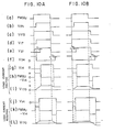
- the voltage detection signal-V 14 is about the same as the inverse of V 24 and is as shown in Fig. 10A at (j).
- the difference PWM U - V 14 and the integral V 173 will be as shown in Fig. 10A at (k) and (1), respectively.
- PWMU and V 14 are, on average, about equal, and the integral is about zero, so that the switch 174 is kept to select the narrower pulses V 171 .
- the switch 174 is selecting the wider pulses V 172 . If the load current is in the direction of the solid arrow in Fig. 6, the voltage detection signal V 14 is as shown in Fig. 10B at (g). PWM u - V 14 will then be, on average, about zero, and the switch 174 is kept unchanged.
- the integrator output V170 alternately becomes positive and negative and the turn-over of the switch 174 is repeated until the manitude of the integrator output diminishes to a substantially small level. In this situation, the actual output voltage of the inverter is, on average, very close to the desired value as commanded by PWM U .
- ⁇ t be equal to or a little larger than the dead time T D - t off .
- the comparator 173 may have a hysteresis characteristic so that the switch 174 is kept unchanged while the integrator output V170 is in a region close to zero. This will prevent too frequent turn-over of the switch 174.
- the integrator 170 may be replaced by an amplifier having a first order lag, and yet a similar result is attained.
- the output voltages of the inverter bridge to be detected need not be those chosen in the above-described embodiment, but can be others, e.g., the voltages across the respective AC terminals and the mid-potential point of the DC terminals P, N, which mid-potential point may be formed by the use of a voltage divider connected across the terminals P, N.
- digital type circuit or digital computer may be used to perform the PWM control. More particularly, a digital counter may be used in place of the integrator 170. Alternatively, an analog integrator may be incorporated in a digital PWM control system. Still alternatively, a digital computor may be used to provide full digital control. Various other combinations can also be adopted.
- the invention is not limited to the specific elements used in the inverter bridge, the specific commutation method or the specific number of phases of the inverter bridge, but is applicable to various types of inverters.
- any deviation of the inverter output voltage from the desired value as commanded by PWM signal is corrected or compensated by the voltage correction circuit, in which a binary signal derived from the detected voltage and the binary PWM signal are compared, and their difference is used to selectively produce a corrected PWM signal which is narrower or wider than the PWM signal, depending on the result of the comparison.
- the system thus operates as a closed loop, i.e., it performs, in a way, a feedback control to bring the inverter output voltage closer to the desired value commanded by the pulse width modulation signal PWM U .
- distortion in the inverter output voltage is minimized and the voltage regulation is improved, and operation of the inverter is therefore stabilized.
- torque ripple is reduced, and efficiency of the motor is improved because the output voltage is closer to sine curve.
Landscapes
- Engineering & Computer Science (AREA)
- Power Engineering (AREA)
- Inverter Devices (AREA)
Applications Claiming Priority (2)
| Application Number | Priority Date | Filing Date | Title |
|---|---|---|---|
| JP187071/83 | 1983-10-07 | ||
| JP58187071A JPH0634594B2 (ja) | 1983-10-07 | 1983-10-07 | 電圧形インバ−タ |
Publications (2)
| Publication Number | Publication Date |
|---|---|
| EP0144593A1 true EP0144593A1 (de) | 1985-06-19 |
| EP0144593B1 EP0144593B1 (de) | 1987-07-08 |
Family
ID=16199622
Family Applications (1)
| Application Number | Title | Priority Date | Filing Date |
|---|---|---|---|
| EP84111725A Expired EP0144593B1 (de) | 1983-10-07 | 1984-10-01 | Steuersystem für einen Wechselrichter vom Spannungstyp |
Country Status (5)
| Country | Link |
|---|---|
| US (1) | US4597037A (de) |
| EP (1) | EP0144593B1 (de) |
| JP (1) | JPH0634594B2 (de) |
| KR (1) | KR890004649B1 (de) |
| DE (1) | DE3464677D1 (de) |
Cited By (3)
| Publication number | Priority date | Publication date | Assignee | Title |
|---|---|---|---|---|
| DE3714174A1 (de) * | 1987-04-24 | 1988-11-10 | Licentia Gmbh | Symmetrierung der abzuschaltenden stroeme parallelgeschalteter, gategesteuerter halbleiter |
| US5274542A (en) * | 1991-02-28 | 1993-12-28 | Kabushiki Kaisha Toshiba | Control device of neutral point clamped power inverter apparatus |
| FR2961977A1 (fr) * | 2010-06-29 | 2011-12-30 | Schneider Toshiba Inverter | Procede de commande et systeme pour compenser les temps-morts dans une commande mli |
Families Citing this family (28)
| Publication number | Priority date | Publication date | Assignee | Title |
|---|---|---|---|---|
| ATE45448T1 (de) * | 1985-05-13 | 1989-08-15 | Siemens Ag | Vorrichtung zur erzeugung eines symmetrischen dreiphasigen spannungssystems mit belastbarem null-leiter. |
| FI77547C (fi) * | 1986-03-19 | 1989-03-10 | Kone Oy | Foerfarande och anordning foer reglering av styrspaenningen vid en trefasig inventer som matar en vaexelstroemmotor. |
| GB2190754A (en) * | 1986-04-11 | 1987-11-25 | Hitachi Ltd | Load current detecting device for pulse width modulation inverter |
| WO1988001467A1 (en) * | 1986-08-15 | 1988-02-25 | Mound Holdings Limited | Fluorescent lamp operation |
| JPH07108097B2 (ja) * | 1987-03-20 | 1995-11-15 | 株式会社日立製作所 | パルス幅変調インバ−タの制御装置 |
| US4823250A (en) * | 1987-11-05 | 1989-04-18 | Picker International, Inc. | Electronic control for light weight, portable x-ray system |
| JP2688487B2 (ja) * | 1987-12-17 | 1997-12-10 | 株式会社日立製作所 | パルス幅変調インバータ制御装置 |
| JP2578159B2 (ja) * | 1988-04-18 | 1997-02-05 | 日本オーチス・エレベータ株式会社 | Pwmインバータ |
| JPH0270290A (ja) * | 1988-08-31 | 1990-03-09 | Mitsubishi Electric Corp | 電動機の制御装置 |
| US5053688A (en) * | 1989-03-07 | 1991-10-01 | Sundstrand Corporation | Feedback circuit for eliminating DC offset in drive current of an AC motor |
| JPH0777516B2 (ja) * | 1989-04-27 | 1995-08-16 | 三菱電機株式会社 | 多相インバータの出力直流分防止装置 |
| US4967336A (en) * | 1990-02-26 | 1990-10-30 | Motorola, Inc. | High voltage bridge interface |
| US5450306A (en) * | 1992-12-07 | 1995-09-12 | Square D Company | Closed loop pulse width modulator inverter with volt-seconds feedback control |
| US5432695A (en) * | 1993-09-17 | 1995-07-11 | The Center For Innovative Technology | Zero-voltage-switched, three-phase PWM rectifier inverter circuit |
| JPH08331882A (ja) * | 1995-03-24 | 1996-12-13 | Seiko Epson Corp | モータ制御装置 |
| US5850132A (en) * | 1997-07-02 | 1998-12-15 | Allin-Bradley Company, Llc | Apparatus used with AC motors for compensating for turn on delay errors |
| DE19845995A1 (de) * | 1998-04-15 | 2000-04-13 | Andreas Boehringer | Stromrichter mit aktiv beeinflußter Kommutierung |
| US6169334B1 (en) | 1998-10-27 | 2001-01-02 | Capstone Turbine Corporation | Command and control system and method for multiple turbogenerators |
| IT1306069B1 (it) * | 1998-11-20 | 2001-05-29 | Zapi Spa | Procedimento di alimentazione di motori asincroni con inverter,inparticolare per veicoli a batteria |
| US6629064B1 (en) | 1999-03-09 | 2003-09-30 | Capstone Turbine Corporation | Apparatus and method for distortion compensation |
| JP3644531B2 (ja) * | 1999-07-06 | 2005-04-27 | 富士電機機器制御株式会社 | オンディレイ補償用アームオン検出回路 |
| US7532723B2 (en) | 2003-11-24 | 2009-05-12 | Interdigital Technology Corporation | Tokens/keys for wireless communications |
| US7548439B2 (en) * | 2005-03-30 | 2009-06-16 | Hitachi, Ltd. | Electric power converter for reducing generated high frequency components |
| US7804379B2 (en) * | 2008-05-07 | 2010-09-28 | Microchip Technology Incorporated | Pulse width modulation dead time compensation method and apparatus |
| DE102009000728A1 (de) * | 2009-02-09 | 2010-10-14 | Biotronik Crm Patent Ag | Verfahren zur Bestimmung einer Stromversorgungs-Zustandsgröße in einem aktiven medizinischen Implantat |
| JP2011087398A (ja) * | 2009-10-15 | 2011-04-28 | Fuji Electric Holdings Co Ltd | ユニットインバータシステム |
| WO2012029451A1 (ja) * | 2010-09-02 | 2012-03-08 | 日立オートモティブシステムズ株式会社 | 同期電動機の駆動システム |
| US9374021B2 (en) | 2013-12-16 | 2016-06-21 | Rockwell Automation Technologies, Inc. | PWM output voltage measurement apparatus and method |
Citations (4)
| Publication number | Priority date | Publication date | Assignee | Title |
|---|---|---|---|---|
| US3967173A (en) * | 1975-03-14 | 1976-06-29 | Allis-Chalmers Corporation | Transistor bridge inverter motor drive having reduced harmonics |
| DE2754241A1 (de) * | 1977-12-06 | 1979-06-07 | Jutronik Gmbh | Statischer frequenzumformer nach dem gleichstrom-zwischenkreis-prinzip zur speisung von drehstrommotoren |
| GB2107945A (en) * | 1981-10-19 | 1983-05-05 | Hughes Tool Co | Motor variable frequency drive |
| EP0116706B1 (de) * | 1982-12-28 | 1986-10-08 | Kabushiki Kaisha Toshiba | Regelsystem für einen Wechselrichter vom Spannungstyp |
Family Cites Families (6)
| Publication number | Priority date | Publication date | Assignee | Title |
|---|---|---|---|---|
| JPS5064730A (de) * | 1973-10-12 | 1975-06-02 | ||
| US3919620A (en) * | 1974-05-22 | 1975-11-11 | Gen Electric | Inverter adaptive lock-out technique |
| DE2446635A1 (de) * | 1974-09-30 | 1976-04-08 | Siemens Ag | Wechselrichteranordnung mit zwei dreiphasigen steuerbaren wechselrichtern |
| US4348734A (en) * | 1980-07-10 | 1982-09-07 | Reliance Electric Company | Converter by stored switching pattern |
| US4445167A (en) * | 1981-10-05 | 1984-04-24 | Tokyo Shibaura Denki Kabushiki Kaisha | Inverter system |
| US4502106A (en) * | 1983-10-17 | 1985-02-26 | Sundstrand Corporation | Current source sine wave inverter |
-
1983
- 1983-10-07 JP JP58187071A patent/JPH0634594B2/ja not_active Expired - Lifetime
-
1984
- 1984-10-01 EP EP84111725A patent/EP0144593B1/de not_active Expired
- 1984-10-01 DE DE8484111725T patent/DE3464677D1/de not_active Expired
- 1984-10-05 US US06/657,881 patent/US4597037A/en not_active Expired - Lifetime
- 1984-10-06 KR KR8406191A patent/KR890004649B1/ko not_active Expired
Patent Citations (4)
| Publication number | Priority date | Publication date | Assignee | Title |
|---|---|---|---|---|
| US3967173A (en) * | 1975-03-14 | 1976-06-29 | Allis-Chalmers Corporation | Transistor bridge inverter motor drive having reduced harmonics |
| DE2754241A1 (de) * | 1977-12-06 | 1979-06-07 | Jutronik Gmbh | Statischer frequenzumformer nach dem gleichstrom-zwischenkreis-prinzip zur speisung von drehstrommotoren |
| GB2107945A (en) * | 1981-10-19 | 1983-05-05 | Hughes Tool Co | Motor variable frequency drive |
| EP0116706B1 (de) * | 1982-12-28 | 1986-10-08 | Kabushiki Kaisha Toshiba | Regelsystem für einen Wechselrichter vom Spannungstyp |
Cited By (5)
| Publication number | Priority date | Publication date | Assignee | Title |
|---|---|---|---|---|
| DE3714174A1 (de) * | 1987-04-24 | 1988-11-10 | Licentia Gmbh | Symmetrierung der abzuschaltenden stroeme parallelgeschalteter, gategesteuerter halbleiter |
| US5274542A (en) * | 1991-02-28 | 1993-12-28 | Kabushiki Kaisha Toshiba | Control device of neutral point clamped power inverter apparatus |
| FR2961977A1 (fr) * | 2010-06-29 | 2011-12-30 | Schneider Toshiba Inverter | Procede de commande et systeme pour compenser les temps-morts dans une commande mli |
| EP2403119A1 (de) * | 2010-06-29 | 2012-01-04 | Schneider Toshiba Inverter Europe SAS | Steuerungsverfahren und System zur Kompensation von Totzeiten für Pulsweitenmodulationssteuerung |
| CN102315822A (zh) * | 2010-06-29 | 2012-01-11 | 施耐德东芝换流器欧洲公司 | 在脉宽调制控制中补偿死区时间的控制方法和系统 |
Also Published As
| Publication number | Publication date |
|---|---|
| DE3464677D1 (en) | 1987-08-13 |
| EP0144593B1 (de) | 1987-07-08 |
| JPS6082066A (ja) | 1985-05-10 |
| KR850003077A (ko) | 1985-05-28 |
| JPH0634594B2 (ja) | 1994-05-02 |
| KR890004649B1 (en) | 1989-11-21 |
| US4597037A (en) | 1986-06-24 |
Similar Documents
| Publication | Publication Date | Title |
|---|---|---|
| US4597037A (en) | Control system for a voltage-type inverter | |
| US4546422A (en) | Control system for a voltage-type inverter | |
| US5428522A (en) | Four quadrant unipolar pulse width modulated inverter | |
| CA2152625C (en) | Closed loop pulse width modulator inverter with volt-seconds feedback control | |
| US4777578A (en) | Integrated current sensor torque control for ac motor drives | |
| KR960001026B1 (ko) | 병렬 구동 피더블유엠(pwm)형 전력 인버팅 장치 사이의 출력 전류 밸런스를 제어하는 회로 및 그 방법 | |
| US5436819A (en) | Apparatus for and method of compensating for an output voltage error in an inverter output | |
| JP4985395B2 (ja) | 電流制御装置とその電流オフセット補正方法 | |
| US4748397A (en) | Control device for choppers parallel between a DC power source and a load for producing balanced chopper currents | |
| EP0152796B1 (de) | Steuervorrichtung für einen Leistungsumrichter | |
| KR100233956B1 (ko) | 전압형 인버터 장치 및 그 제어방법 | |
| KR920010235B1 (ko) | 펄스폭 변조승압 변환기의 제어장치 | |
| US5208524A (en) | Current control apparatus for PWM control | |
| US20240305216A1 (en) | Arrangement For Current Sharing Of Parallel-Connected Inverters | |
| JPH0698557A (ja) | パルス幅変調制御インバータの制御回路 | |
| JP3070314B2 (ja) | インバータの出力電圧補償回路 | |
| JPH049036B2 (de) | ||
| JP2577514B2 (ja) | 中性点クランプ式電力変換器の制御方法 | |
| JP3397138B2 (ja) | インバータ装置 | |
| JP3264451B2 (ja) | 瞬時電流制御型pwmインバータ | |
| KR19980057561U (ko) | 인버터의 데드 타임 보상장치 | |
| JPH04295279A (ja) | 中性点クランプ式電力変換器の制御装置 | |
| JPS6212396A (ja) | チヨツパの相電流制御装置 | |
| EP1197757A2 (de) | Wechselrichter | |
| JPH0667216B2 (ja) | インバータ装置 |
Legal Events
| Date | Code | Title | Description |
|---|---|---|---|
| PUAI | Public reference made under article 153(3) epc to a published international application that has entered the european phase |
Free format text: ORIGINAL CODE: 0009012 |
|
| 17P | Request for examination filed |
Effective date: 19841030 |
|
| AK | Designated contracting states |
Designated state(s): DE FR GB SE |
|
| 17Q | First examination report despatched |
Effective date: 19860507 |
|
| GRAA | (expected) grant |
Free format text: ORIGINAL CODE: 0009210 |
|
| AK | Designated contracting states |
Kind code of ref document: B1 Designated state(s): DE FR GB SE |
|
| REF | Corresponds to: |
Ref document number: 3464677 Country of ref document: DE Date of ref document: 19870813 |
|
| ET | Fr: translation filed | ||
| PLBE | No opposition filed within time limit |
Free format text: ORIGINAL CODE: 0009261 |
|
| STAA | Information on the status of an ep patent application or granted ep patent |
Free format text: STATUS: NO OPPOSITION FILED WITHIN TIME LIMIT |
|
| 26N | No opposition filed | ||
| EAL | Se: european patent in force in sweden |
Ref document number: 84111725.2 |
|
| REG | Reference to a national code |
Ref country code: GB Ref legal event code: 746 Effective date: 19980909 |
|
| REG | Reference to a national code |
Ref country code: FR Ref legal event code: D6 |
|
| REG | Reference to a national code |
Ref country code: GB Ref legal event code: IF02 |
|
| PGFP | Annual fee paid to national office [announced via postgrant information from national office to epo] |
Ref country code: GB Payment date: 20031001 Year of fee payment: 20 |
|
| PGFP | Annual fee paid to national office [announced via postgrant information from national office to epo] |
Ref country code: FR Payment date: 20031003 Year of fee payment: 20 |
|
| PGFP | Annual fee paid to national office [announced via postgrant information from national office to epo] |
Ref country code: SE Payment date: 20031007 Year of fee payment: 20 |
|
| PGFP | Annual fee paid to national office [announced via postgrant information from national office to epo] |
Ref country code: DE Payment date: 20031009 Year of fee payment: 20 |
|
| PG25 | Lapsed in a contracting state [announced via postgrant information from national office to epo] |
Ref country code: GB Free format text: LAPSE BECAUSE OF EXPIRATION OF PROTECTION Effective date: 20040930 |
|
| REG | Reference to a national code |
Ref country code: GB Ref legal event code: PE20 |
|
| EUG | Se: european patent has lapsed |