EP0145520B1 - Bildschirm mit aktiver Matrix ohne Kreuzung von Zeilen- und Spaltenadressenleitungen - Google Patents
Bildschirm mit aktiver Matrix ohne Kreuzung von Zeilen- und Spaltenadressenleitungen Download PDFInfo
- Publication number
- EP0145520B1 EP0145520B1 EP84401967A EP84401967A EP0145520B1 EP 0145520 B1 EP0145520 B1 EP 0145520B1 EP 84401967 A EP84401967 A EP 84401967A EP 84401967 A EP84401967 A EP 84401967A EP 0145520 B1 EP0145520 B1 EP 0145520B1
- Authority
- EP
- European Patent Office
- Prior art keywords
- row
- column
- conductors
- display screen
- image points
- Prior art date
- Legal status (The legal status is an assumption and is not a legal conclusion. Google has not performed a legal analysis and makes no representation as to the accuracy of the status listed.)
- Expired
Links
Images
Classifications
-
- G—PHYSICS
- G02—OPTICS
- G02F—OPTICAL DEVICES OR ARRANGEMENTS FOR THE CONTROL OF LIGHT BY MODIFICATION OF THE OPTICAL PROPERTIES OF THE MEDIA OF THE ELEMENTS INVOLVED THEREIN; NON-LINEAR OPTICS; FREQUENCY-CHANGING OF LIGHT; OPTICAL LOGIC ELEMENTS; OPTICAL ANALOGUE/DIGITAL CONVERTERS
- G02F1/00—Devices or arrangements for the control of the intensity, colour, phase, polarisation or direction of light arriving from an independent light source, e.g. switching, gating or modulating; Non-linear optics
- G02F1/01—Devices or arrangements for the control of the intensity, colour, phase, polarisation or direction of light arriving from an independent light source, e.g. switching, gating or modulating; Non-linear optics for the control of the intensity, phase, polarisation or colour
- G02F1/13—Devices or arrangements for the control of the intensity, colour, phase, polarisation or direction of light arriving from an independent light source, e.g. switching, gating or modulating; Non-linear optics for the control of the intensity, phase, polarisation or colour based on liquid crystals, e.g. single liquid crystal display cells
- G02F1/133—Constructional arrangements; Operation of liquid crystal cells; Circuit arrangements
- G02F1/136—Liquid crystal cells structurally associated with a semi-conducting layer or substrate, e.g. cells forming part of an integrated circuit
- G02F1/1362—Active matrix addressed cells
- G02F1/1368—Active matrix addressed cells in which the switching element is a three-electrode device
-
- G—PHYSICS
- G02—OPTICS
- G02F—OPTICAL DEVICES OR ARRANGEMENTS FOR THE CONTROL OF LIGHT BY MODIFICATION OF THE OPTICAL PROPERTIES OF THE MEDIA OF THE ELEMENTS INVOLVED THEREIN; NON-LINEAR OPTICS; FREQUENCY-CHANGING OF LIGHT; OPTICAL LOGIC ELEMENTS; OPTICAL ANALOGUE/DIGITAL CONVERTERS
- G02F1/00—Devices or arrangements for the control of the intensity, colour, phase, polarisation or direction of light arriving from an independent light source, e.g. switching, gating or modulating; Non-linear optics
- G02F1/01—Devices or arrangements for the control of the intensity, colour, phase, polarisation or direction of light arriving from an independent light source, e.g. switching, gating or modulating; Non-linear optics for the control of the intensity, phase, polarisation or colour
- G02F1/13—Devices or arrangements for the control of the intensity, colour, phase, polarisation or direction of light arriving from an independent light source, e.g. switching, gating or modulating; Non-linear optics for the control of the intensity, phase, polarisation or colour based on liquid crystals, e.g. single liquid crystal display cells
- G02F1/133—Constructional arrangements; Operation of liquid crystal cells; Circuit arrangements
- G02F1/136—Liquid crystal cells structurally associated with a semi-conducting layer or substrate, e.g. cells forming part of an integrated circuit
- G02F1/1362—Active matrix addressed cells
-
- G—PHYSICS
- G09—EDUCATION; CRYPTOGRAPHY; DISPLAY; ADVERTISING; SEALS
- G09G—ARRANGEMENTS OR CIRCUITS FOR CONTROL OF INDICATING DEVICES USING STATIC MEANS TO PRESENT VARIABLE INFORMATION
- G09G3/00—Control arrangements or circuits, of interest only in connection with visual indicators other than cathode-ray tubes
- G09G3/20—Control arrangements or circuits, of interest only in connection with visual indicators other than cathode-ray tubes for presentation of an assembly of a number of characters, e.g. a page, by composing the assembly by combination of individual elements arranged in a matrix no fixed position being assigned to or needed to be assigned to the individual characters or partial characters
- G09G3/34—Control arrangements or circuits, of interest only in connection with visual indicators other than cathode-ray tubes for presentation of an assembly of a number of characters, e.g. a page, by composing the assembly by combination of individual elements arranged in a matrix no fixed position being assigned to or needed to be assigned to the individual characters or partial characters by control of light from an independent source
- G09G3/36—Control arrangements or circuits, of interest only in connection with visual indicators other than cathode-ray tubes for presentation of an assembly of a number of characters, e.g. a page, by composing the assembly by combination of individual elements arranged in a matrix no fixed position being assigned to or needed to be assigned to the individual characters or partial characters by control of light from an independent source using liquid crystals
- G09G3/3611—Control of matrices with row and column drivers
- G09G3/3648—Control of matrices with row and column drivers using an active matrix
- G09G3/3655—Details of drivers for counter electrodes, e.g. common electrodes for pixel capacitors or supplementary storage capacitors
-
- G—PHYSICS
- G02—OPTICS
- G02F—OPTICAL DEVICES OR ARRANGEMENTS FOR THE CONTROL OF LIGHT BY MODIFICATION OF THE OPTICAL PROPERTIES OF THE MEDIA OF THE ELEMENTS INVOLVED THEREIN; NON-LINEAR OPTICS; FREQUENCY-CHANGING OF LIGHT; OPTICAL LOGIC ELEMENTS; OPTICAL ANALOGUE/DIGITAL CONVERTERS
- G02F2201/00—Constructional arrangements not provided for in groups G02F1/00 - G02F7/00
- G02F2201/12—Constructional arrangements not provided for in groups G02F1/00 - G02F7/00 electrode
- G02F2201/122—Constructional arrangements not provided for in groups G02F1/00 - G02F7/00 electrode having a particular pattern
-
- G—PHYSICS
- G09—EDUCATION; CRYPTOGRAPHY; DISPLAY; ADVERTISING; SEALS
- G09G—ARRANGEMENTS OR CIRCUITS FOR CONTROL OF INDICATING DEVICES USING STATIC MEANS TO PRESENT VARIABLE INFORMATION
- G09G3/00—Control arrangements or circuits, of interest only in connection with visual indicators other than cathode-ray tubes
- G09G3/20—Control arrangements or circuits, of interest only in connection with visual indicators other than cathode-ray tubes for presentation of an assembly of a number of characters, e.g. a page, by composing the assembly by combination of individual elements arranged in a matrix no fixed position being assigned to or needed to be assigned to the individual characters or partial characters
- G09G3/2007—Display of intermediate tones
- G09G3/2011—Display of intermediate tones by amplitude modulation
Definitions
- the present invention relates to an active matrix display screen without crossing the row and column addressing conductors. It finds an application in optoelectronics in the production of liquid crystal displays used in particular as converters of electrical information into optical information.
- a known type of solution consists in incorporating the electrical threshold and the memory effect at each image point.
- This threshold can be ensured by a thin film transistor, by a varistor or by a MIM (metal-insulator-metal) switch, or the like.
- MIM metal-insulator-metal
- each image point is therefore located at the intersection of a line and a connection column and it consists of a transistor, for example, and a capacitor.
- the armatures of the capacitor can be formed by the electrodes of the liquid crystal cell itself.
- the image point is therefore reduced to a transistor and to a capacitor, one of the armatures of which is formed by the electrode placed on the wall of the cell which contains the transistor, the other armature being constituted of the counter-electrode. arranged on the other wall of the cell.
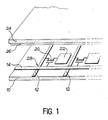
- FIG. 1 Such a structure is shown in FIG. 1.
- a lower wall 10 carrying conductive columns 12 and conductive lines 14, a thin film transistor 20 and a transparent electrode 22, and on the other hand, an upper wall 24 covered with a counter-electrode 26 also transparent.
- the structure described in application EP-A-070 598 comprises two support plates between which an optoelectronic transducer is placed.
- a structure which moreover comprises switching elements produced from head-to-tail diodes, does not make it possible to obtain an active matrix architecture in which the switching elements are transistors and in which the line and column crossovers of the display screen.
- the invention provides an active de-matrix architecture eliminating these crossings of row and column conductors.
- the invention replaces the counter-electrode on the upper face with a family of column electrodes.
- the underside no longer supports the conductive columns.
- the crossings of conductive rows and columns being eliminated, the short-circuits are eliminated and the production efficiency of such an active matrix is significantly increased.
- the first wall contains all the slow logic produced for example in hydrogenated Si and the second wall contains all the fast logic produced for example in polycrystalline Si whereas in the prior art these two technologies are produced on the same substrate .
- the subject of the invention is therefore an active matrix display screen comprising a material whose optical characteristic can be modified, this material being interposed between a first wall and a second transparent wall, said screen comprising a plurality of image points arranged in a matrix of pxq elements, where 1 ⁇ p and 1 ⁇ q, a first family of p addressing conductors of a row of image points, a second family of q addressing conductors of a column of picture points, each image point consisting of a switching element and a capacitor formed by two electrodes each disposed on one of the two walls, the first wall of said screen carrying a matrix of elements each consisting of the switching element and of an electrode and carrying the first family of p row conductors and the second transparent wall carrying a family of q column electrodes and the second family of q column conductors, the electrodes and conductors of the same rank being interconnected, said screen being characterized in that the switching element of each image point is a thin film transistor whose gate is connected to a line conductor
- each line of image points is associated with a line conductor disposed on one side of said line of image points and parallel to it, and a conductor brought to the constant potential and arranged parallel to said line of image points, on the other side thereof.
- the average value of the signal applied to each column electrode is constant over the period of a frame.
- the width Tc of the slot of the signal applied to each column electrode during the time TL for addressing a line is equal to ⁇ L / 2.
- the line addressing signal contains, during each frame, a single slot of width TL / 2.
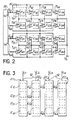
- FIG. 2 shows the elements of the active matrix produced on one of the paroids of a display screen according to the invention.
- This screen includes 16 image points arranged in a 4x4 matrix.
- Each element 30 constitutes a part of an image point.
- Each of these elements consists of a thin film transistor denoted T and an electrode denoted E. These transistor and electrode are conventionally represented by subscript figures indicating their row and column number in the matrix.
- V Gi The potential applied on the ith line, where 1 ⁇ i ⁇ 4, is noted V Gi .
- This line potential is delivered by a shift register 32 which delivers a voltage slot successively on each of the line conductors 14.
- each transistor in the matrix is connected to a constant potential V s .
- This potential acts as a charge source for each of the electrodes of the elements 30 whose transistor is activated by a voltage pulse on its gate.
- FIG. 3 represents the part of the active matrix of a display screen produced on the other wall of this screen.
- 4 column electrodes EC, EC 2 , EC 3 , EC 4 were produced .
- Each of these electrodes is connected to a column conductor 12.
- each display point of an image point therefore consists of the area where an electrode of one wall and an electrode of the other wall are superimposed. These display points are in fact geometrically coincident with the electrodes of the first wall.
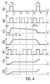
- FIG. 4a represents the voltage V G1 applied to the gate of the transistors of the first line, that is to say on the transistors T 11 , T, 2 , T 13 and T 14 .
- the time axis is divided into intervals of constant length.
- the time interval between the dates 0 and t 4 corresponds to a frame, that is to say to the addressing time of all the image points.
- the length ⁇ L is equal to the duration of the addressing of a line of the screen. Each point of the line is in fact only activated during the time interval T , during which the line voltage V G1 is not zero.
- this time interval T is at least equal to half the time interval TL for addressing the line.
- FIG. 4b represents the voltage V C1 applied to the electrode EC, (FIG. 3) as a function of the time.
- This potential V C1 or more exactly the difference between the potential V C1 , and the constant source potential V S determines, when the first line of transistor is addressed, the charge of the image point located at the intersection of the first line and the first column.
- the signal V C1 consists of a slot of width- ⁇ c in each time interval TL .
- the slots in dashed lines correspond to the addressing of the image points located at the intersection of the first column and, respectively, of the second, third and fourth lines.
- the position of the slot of the signal V C1 , in the interval ⁇ L determines the gray level of the image point.
- FIG. 4c shows the charge Q 11 of the capacitor constituting the display point located at the intersection of the first line and the first column.
- the signal V G1 does not exhibit a voltage pulse.
- the charge Q 11 is therefore retained.
- the charge of the capacitor is modified.
- the column signal V C1 then being zero at this instant, the capacitor discharges.
- FIG. 4d The optical aspect related to the capacitive effect shown in Figure 4c is illustrated in Figure 4d.
- the curve in this figure represents the gray level of the image point. At the initial instant, the point is black, then when the capacity charges the image point becomes white. It becomes black again when the capacity discharges between instants t 4 and t s .
- Figures 4d, 4e and 4f represent, for the image point located at the intersection of the first line and the second column, respectively the same curves as those represented in 4b, 4c and 4d for the image point located at the intersection of the first row and the first column.
- the voltage pulse of signal V c2 applied to the second column electrode between times 0 and t 1 partially covers the voltage pulse applied during this same instant to signal V G1 . This results in a partial charge on the Q 12 Consensor of the image point. This charge is not altered, apart from capacity leaks, until a new voltage window appears on the signal V G1 . This occurs between instants t 4 and t s . The voltage slot appearing in this time interval on the column signal V C2 completely covers the voltage slot of the signal V G1 . The image point capacitor therefore charges fully.
- the image point changes from black to a gray level between the instants of start and end of the voltage slot on the signal V G1 . It then passes from this gray level to the white level between the instants of start and end of the consecutive voltage pulse of the signal V G1 .
Landscapes
- Physics & Mathematics (AREA)
- Engineering & Computer Science (AREA)
- Chemical & Material Sciences (AREA)
- Crystallography & Structural Chemistry (AREA)
- Nonlinear Science (AREA)
- General Physics & Mathematics (AREA)
- Mathematical Physics (AREA)
- Microelectronics & Electronic Packaging (AREA)
- Theoretical Computer Science (AREA)
- Computer Hardware Design (AREA)
- Optics & Photonics (AREA)
- Power Engineering (AREA)
- Liquid Crystal (AREA)
- Devices For Indicating Variable Information By Combining Individual Elements (AREA)
- Control Of Indicators Other Than Cathode Ray Tubes (AREA)
- Liquid Crystal Display Device Control (AREA)
Claims (4)
Applications Claiming Priority (2)
| Application Number | Priority Date | Filing Date | Title |
|---|---|---|---|
| FR8315996 | 1983-10-07 | ||
| FR8315996A FR2553218B1 (fr) | 1983-10-07 | 1983-10-07 | Ecran d'affichage a matrice active sans croisement des lignes et des colonnes d'adressage |
Publications (3)
| Publication Number | Publication Date |
|---|---|
| EP0145520A2 EP0145520A2 (de) | 1985-06-19 |
| EP0145520A3 EP0145520A3 (en) | 1985-07-10 |
| EP0145520B1 true EP0145520B1 (de) | 1989-01-04 |
Family
ID=9292929
Family Applications (1)
| Application Number | Title | Priority Date | Filing Date |
|---|---|---|---|
| EP84401967A Expired EP0145520B1 (de) | 1983-10-07 | 1984-10-02 | Bildschirm mit aktiver Matrix ohne Kreuzung von Zeilen- und Spaltenadressenleitungen |
Country Status (5)
| Country | Link |
|---|---|
| US (1) | US4694287A (de) |
| EP (1) | EP0145520B1 (de) |
| JP (1) | JPS60107690A (de) |
| DE (1) | DE3475975D1 (de) |
| FR (1) | FR2553218B1 (de) |
Families Citing this family (27)
| Publication number | Priority date | Publication date | Assignee | Title |
|---|---|---|---|---|
| DE3581498D1 (de) * | 1984-11-16 | 1991-02-28 | Matsushita Electric Industrial Co Ltd | Aktive matrixschaltung fuer fluessigkristallanzeigen. |
| US4678282A (en) * | 1985-02-19 | 1987-07-07 | Ovonic Imaging Systems, Inc. | Active display matrix addressable without crossed lines on any one substrate and method of using the same |
| GB8508656D0 (en) * | 1985-04-03 | 1985-05-09 | Gen Electric Co Plc | Liquid crystal displays |
| JPS62108227A (ja) * | 1985-10-31 | 1987-05-19 | インタ−ナショナル ビジネス マシ−ンズ コ−ポレ−ション | デイスプレイ装置 |
| FR2590394B1 (fr) * | 1985-11-15 | 1987-12-18 | Thomson Csf | Ecran de visualisation electro-optique a transistors de commande |
| FR2593632B1 (fr) * | 1986-01-27 | 1988-03-18 | Maurice Francois | Ecran d'affichage a matrice active et procedes de realisation de cet ecran |
| DE3750855T2 (de) * | 1986-02-21 | 1995-05-24 | Canon Kk | Anzeigegerät. |
| KR900004989B1 (en) * | 1986-09-11 | 1990-07-16 | Fujitsu Ltd | Active matrix type display and driving method |
| FR2606194B1 (fr) * | 1986-11-05 | 1989-02-17 | Commissariat Energie Atomique | Dispositif d'affichage matriciel et procede de commande de ce dispositif |
| FR2614718B1 (fr) * | 1987-04-28 | 1989-06-16 | Commissariat Energie Atomique | Ecran matriciel d'affichage a cristaux liquides muni de capacites de stockage |
| FR2625827B1 (fr) * | 1988-01-11 | 1993-07-16 | Commissariat Energie Atomique | Ecran d'affichage en couleur a matrice active sans croisement des conducteurs lignes d'adressage et des conducteurs colonnes de commande |
| US4968119A (en) * | 1989-01-10 | 1990-11-06 | David Sarnoff Research Center, Inc. | High-density liquid-crystal active dot-matrix display structure |
| KR940005240B1 (ko) * | 1990-05-07 | 1994-06-15 | 후지스 가부시끼가이샤 | 고성능 엑티브 매트릭스(active matrix)형 표시장치 |
| KR970009405B1 (en) * | 1991-10-05 | 1997-06-13 | Fujitsu Ltd | Active matrix type display device |
| US5493439A (en) * | 1992-09-29 | 1996-02-20 | Engle; Craig D. | Enhanced surface deformation light modulator |
| US5488505A (en) * | 1992-10-01 | 1996-01-30 | Engle; Craig D. | Enhanced electrostatic shutter mosaic modulator |
| US5561548A (en) * | 1992-10-07 | 1996-10-01 | Engle; Craig D. | Enhanced membrane light modulator |
| US5521746A (en) * | 1993-02-22 | 1996-05-28 | Engle; Craig D. | Poppet valve modulator |
| JP3300282B2 (ja) | 1998-04-30 | 2002-07-08 | シャープ株式会社 | 液晶表示装置および液晶表示装置の製造方法 |
| JP3519310B2 (ja) * | 1998-06-12 | 2004-04-12 | シャープ株式会社 | 液晶表示装置 |
| JP3699850B2 (ja) | 1999-01-29 | 2005-09-28 | シャープ株式会社 | 表示装置および液晶表示装置 |
| JP3658260B2 (ja) | 1999-04-30 | 2005-06-08 | シャープ株式会社 | 液晶表示装置 |
| JP3527168B2 (ja) | 1999-06-02 | 2004-05-17 | シャープ株式会社 | 液晶表示装置 |
| US7088330B2 (en) | 2000-12-25 | 2006-08-08 | Sharp Kabushiki Kaisha | Active matrix substrate, display device and method for driving the display device |
| JP2003216062A (ja) * | 2002-01-18 | 2003-07-30 | Sharp Corp | 表示装置 |
| KR101407372B1 (ko) | 2006-07-11 | 2014-06-17 | 코닌클리케 필립스 엔.브이. | 디스플레이를 위한 개선된 전극 레이아웃 |
| WO2011111404A1 (ja) * | 2010-03-10 | 2011-09-15 | シャープ株式会社 | 表示装置 |
Family Cites Families (11)
| Publication number | Priority date | Publication date | Assignee | Title |
|---|---|---|---|---|
| US4233602A (en) * | 1977-03-30 | 1980-11-11 | Hitachi, Ltd. | Multi-matrix display system having matrix display panel with uncrossed connections on substrates |
| US4110664A (en) * | 1977-04-15 | 1978-08-29 | Westinghouse Electric Corp. | Electroluminescent bargraph with integral thin-film transistor control circuitry |
| US4233603A (en) * | 1978-11-16 | 1980-11-11 | General Electric Company | Multiplexed varistor-controlled liquid crystal display |
| DE3071167D1 (en) * | 1979-08-03 | 1985-11-14 | Hughes Aircraft Co | Method and apparatus for multi-mode image display with a liquid crystal light valve |
| JPS5691277A (en) * | 1979-12-25 | 1981-07-24 | Citizen Watch Co Ltd | Liquiddcrystal display panel |
| EP0034796B1 (de) * | 1980-02-22 | 1987-09-16 | Kabushiki Kaisha Toshiba | Flüssigkristall-Anzeigevorrichtung |
| JPS575083A (en) * | 1980-06-13 | 1982-01-11 | Tokyo Shibaura Electric Co | Display unit |
| FR2499744B1 (fr) * | 1981-01-05 | 1986-07-04 | Commissariat Energie Atomique | Dispositif d'affichage matriciel comprenant deux familles d'electrodes lignes et son procede de commande |
| JPS57201295A (en) * | 1981-06-04 | 1982-12-09 | Sony Corp | Two-dimensional address device |
| NL8103376A (nl) * | 1981-07-16 | 1983-02-16 | Philips Nv | Weergeefinrichting. |
| US4406997A (en) * | 1981-09-30 | 1983-09-27 | International Business Machines Corporation | Method and means for minimizing the effect of short circuits in flat panel displays |
-
1983
- 1983-10-07 FR FR8315996A patent/FR2553218B1/fr not_active Expired
-
1984
- 1984-10-02 DE DE8484401967T patent/DE3475975D1/de not_active Expired
- 1984-10-02 EP EP84401967A patent/EP0145520B1/de not_active Expired
- 1984-10-05 JP JP59209605A patent/JPS60107690A/ja active Pending
- 1984-10-05 US US06/658,049 patent/US4694287A/en not_active Expired - Fee Related
Also Published As
| Publication number | Publication date |
|---|---|
| FR2553218A1 (fr) | 1985-04-12 |
| EP0145520A2 (de) | 1985-06-19 |
| EP0145520A3 (en) | 1985-07-10 |
| JPS60107690A (ja) | 1985-06-13 |
| DE3475975D1 (en) | 1989-02-09 |
| FR2553218B1 (fr) | 1987-09-25 |
| US4694287A (en) | 1987-09-15 |
Similar Documents
| Publication | Publication Date | Title |
|---|---|---|
| EP0145520B1 (de) | Bildschirm mit aktiver Matrix ohne Kreuzung von Zeilen- und Spaltenadressenleitungen | |
| US4223308A (en) | LCDs (Liquid crystal displays) controlled by thin film diode switches | |
| FR2507803A1 (fr) | Dispositif d'affichage en matrice a cristaux liquides | |
| EP0289415B1 (de) | Flüssigkristall-Matrix-Anzeigeschirm, Versehen mit Speicherkapazität | |
| US4251136A (en) | LCDs (Liquid crystal displays) controlled by thin film diode switches | |
| FR2542119A1 (fr) | Procede pour commander un ecran d'affichage matriciel a cristaux liquides | |
| FR2488013A1 (fr) | Dispositif a matrice d'elements actifs | |
| EP0332476B1 (de) | Aktiver Matrix-Farbbildschirm ohne Kreuzung der Leiterbahnen für Adressierung und Spaltensteuerung | |
| EP2439583A1 (de) | Flüssigkristallanzeige vom transmissiven Typ in CMOS-Technologie mit zusätzlicher Speicherkapazität | |
| EP0228317B1 (de) | Elektrooptischer Anzeigeschirm mit Steuertransistoren | |
| EP0246945B1 (de) | Elektro-optischer Anzeigeschirm und sein Herstellungsverfahren | |
| EP0058593B1 (de) | Matrixanzeigevorrichtung mit verschiedenen Arten von Elektroden und Verfahren zu ihrer Ansteuerung | |
| EP0487389A1 (de) | Flacher Bildschirm mit aktiver Matrix | |
| KR101942971B1 (ko) | 낮은 소비전력을 갖는 전기습윤 디스플레이 장치 및 전기습윤 디스플레이 장치의 구동 방법 | |
| FR2772501A1 (fr) | Dispositif de commande matriciel | |
| EP0506528B1 (de) | Matrix-Ansteuerungsstruktur für Anzeigeschirm | |
| WO2012175250A1 (fr) | Afficheur a cristal liquide a electrodes d'effacement | |
| EP0202992B1 (de) | Anzeigevorrichtung mit aktiver Matrix-Anordnung und integrierter Ansteuerung | |
| EP0564337A1 (de) | Anzeigeschirm mit optischer Maske und Verfahren zur Verwirklichung dieses Schirms | |
| US4662719A (en) | Liquid crystal display and method for production | |
| EP0152708B1 (de) | Verfahren und Einrichtung zum Steuern einer Rasterbildanzeigeeinrichtung | |
| FR2605778A1 (fr) | Panneau de visualisation a cristaux liquides et procede d'inscription des donnees sur ce panneau | |
| FR2488016A1 (fr) | Module elementaire pour panneau d'affichage matriciel et panneau d'affichage comportant un tel module | |
| EP0256927B1 (de) | Matrix-Anzeigevorrichtung mit zwei Gruppen von Zeilen- und zwei Spaltenelektroden je Bildelement und ihr Steuerungsverfahren | |
| WO2003073406A1 (fr) | Moyens d'alimentation et de pilotage pour panneau a plasma utilisant des transformateurs. |
Legal Events
| Date | Code | Title | Description |
|---|---|---|---|
| PUAI | Public reference made under article 153(3) epc to a published international application that has entered the european phase |
Free format text: ORIGINAL CODE: 0009012 |
|
| PUAL | Search report despatched |
Free format text: ORIGINAL CODE: 0009013 |
|
| AK | Designated contracting states |
Designated state(s): CH DE GB IT LI NL SE |
|
| AK | Designated contracting states |
Designated state(s): CH DE GB IT LI NL SE |
|
| 17P | Request for examination filed |
Effective date: 19851212 |
|
| 17Q | First examination report despatched |
Effective date: 19870812 |
|
| RAP1 | Party data changed (applicant data changed or rights of an application transferred) |
Owner name: COMMISSARIAT A L'ENERGIE ATOMIQUE |
|
| GRAA | (expected) grant |
Free format text: ORIGINAL CODE: 0009210 |
|
| AK | Designated contracting states |
Kind code of ref document: B1 Designated state(s): CH DE GB IT LI NL SE |
|
| ITF | It: translation for a ep patent filed | ||
| REF | Corresponds to: |
Ref document number: 3475975 Country of ref document: DE Date of ref document: 19890209 |
|
| GBT | Gb: translation of ep patent filed (gb section 77(6)(a)/1977) | ||
| PLBE | No opposition filed within time limit |
Free format text: ORIGINAL CODE: 0009261 |
|
| STAA | Information on the status of an ep patent application or granted ep patent |
Free format text: STATUS: NO OPPOSITION FILED WITHIN TIME LIMIT |
|
| 26N | No opposition filed | ||
| PGFP | Annual fee paid to national office [announced via postgrant information from national office to epo] |
Ref country code: SE Payment date: 19910920 Year of fee payment: 8 |
|
| PGFP | Annual fee paid to national office [announced via postgrant information from national office to epo] |
Ref country code: CH Payment date: 19911004 Year of fee payment: 8 |
|
| ITTA | It: last paid annual fee | ||
| PG25 | Lapsed in a contracting state [announced via postgrant information from national office to epo] |
Ref country code: SE Effective date: 19921003 |
|
| PG25 | Lapsed in a contracting state [announced via postgrant information from national office to epo] |
Ref country code: LI Effective date: 19921031 Ref country code: CH Effective date: 19921031 |
|
| REG | Reference to a national code |
Ref country code: CH Ref legal event code: PL |
|
| PGFP | Annual fee paid to national office [announced via postgrant information from national office to epo] |
Ref country code: DE Payment date: 19930925 Year of fee payment: 10 |
|
| PGFP | Annual fee paid to national office [announced via postgrant information from national office to epo] |
Ref country code: GB Payment date: 19930929 Year of fee payment: 10 |
|
| PGFP | Annual fee paid to national office [announced via postgrant information from national office to epo] |
Ref country code: NL Payment date: 19931031 Year of fee payment: 10 |
|
| PG25 | Lapsed in a contracting state [announced via postgrant information from national office to epo] |
Ref country code: GB Effective date: 19941002 |
|
| EUG | Se: european patent has lapsed |
Ref document number: 84401967.9 Effective date: 19930510 |
|
| PG25 | Lapsed in a contracting state [announced via postgrant information from national office to epo] |
Ref country code: NL Effective date: 19950501 |
|
| GBPC | Gb: european patent ceased through non-payment of renewal fee |
Effective date: 19941002 |
|
| NLV4 | Nl: lapsed or anulled due to non-payment of the annual fee | ||
| PG25 | Lapsed in a contracting state [announced via postgrant information from national office to epo] |
Ref country code: DE Effective date: 19950701 |