EP0332476B1 - Aktiver Matrix-Farbbildschirm ohne Kreuzung der Leiterbahnen für Adressierung und Spaltensteuerung - Google Patents
Aktiver Matrix-Farbbildschirm ohne Kreuzung der Leiterbahnen für Adressierung und Spaltensteuerung Download PDFInfo
- Publication number
- EP0332476B1 EP0332476B1 EP89400053A EP89400053A EP0332476B1 EP 0332476 B1 EP0332476 B1 EP 0332476B1 EP 89400053 A EP89400053 A EP 89400053A EP 89400053 A EP89400053 A EP 89400053A EP 0332476 B1 EP0332476 B1 EP 0332476B1
- Authority
- EP
- European Patent Office
- Prior art keywords
- conductor
- wall
- conductors
- electrode
- electrodes
- Prior art date
- Legal status (The legal status is an assumption and is not a legal conclusion. Google has not performed a legal analysis and makes no representation as to the accuracy of the status listed.)
- Expired - Lifetime
Links
- 239000004020 conductor Substances 0.000 title claims description 49
- 239000011159 matrix material Substances 0.000 title claims description 7
- 239000010409 thin film Substances 0.000 claims description 10
- 239000004973 liquid crystal related substance Substances 0.000 claims description 7
- 239000003990 capacitor Substances 0.000 claims description 5
- 238000004519 manufacturing process Methods 0.000 description 5
- 239000003086 colorant Substances 0.000 description 3
- 229910021417 amorphous silicon Inorganic materials 0.000 description 2
- 238000010586 diagram Methods 0.000 description 2
- 238000004070 electrodeposition Methods 0.000 description 2
- 238000000034 method Methods 0.000 description 2
- 230000003071 parasitic effect Effects 0.000 description 2
- 230000000694 effects Effects 0.000 description 1
- 238000011156 evaluation Methods 0.000 description 1
- 230000002349 favourable effect Effects 0.000 description 1
- 230000000007 visual effect Effects 0.000 description 1
Images

Classifications
-
- G—PHYSICS
- G02—OPTICS
- G02F—OPTICAL DEVICES OR ARRANGEMENTS FOR THE CONTROL OF LIGHT BY MODIFICATION OF THE OPTICAL PROPERTIES OF THE MEDIA OF THE ELEMENTS INVOLVED THEREIN; NON-LINEAR OPTICS; FREQUENCY-CHANGING OF LIGHT; OPTICAL LOGIC ELEMENTS; OPTICAL ANALOGUE/DIGITAL CONVERTERS
- G02F1/00—Devices or arrangements for the control of the intensity, colour, phase, polarisation or direction of light arriving from an independent light source, e.g. switching, gating or modulating; Non-linear optics
- G02F1/01—Devices or arrangements for the control of the intensity, colour, phase, polarisation or direction of light arriving from an independent light source, e.g. switching, gating or modulating; Non-linear optics for the control of the intensity, phase, polarisation or colour
- G02F1/13—Devices or arrangements for the control of the intensity, colour, phase, polarisation or direction of light arriving from an independent light source, e.g. switching, gating or modulating; Non-linear optics for the control of the intensity, phase, polarisation or colour based on liquid crystals, e.g. single liquid crystal display cells
- G02F1/133—Constructional arrangements; Operation of liquid crystal cells; Circuit arrangements
- G02F1/1333—Constructional arrangements; Manufacturing methods
- G02F1/1335—Structural association of cells with optical devices, e.g. polarisers or reflectors
- G02F1/133509—Filters, e.g. light shielding masks
- G02F1/133514—Colour filters
-
- G—PHYSICS
- G02—OPTICS
- G02F—OPTICAL DEVICES OR ARRANGEMENTS FOR THE CONTROL OF LIGHT BY MODIFICATION OF THE OPTICAL PROPERTIES OF THE MEDIA OF THE ELEMENTS INVOLVED THEREIN; NON-LINEAR OPTICS; FREQUENCY-CHANGING OF LIGHT; OPTICAL LOGIC ELEMENTS; OPTICAL ANALOGUE/DIGITAL CONVERTERS
- G02F1/00—Devices or arrangements for the control of the intensity, colour, phase, polarisation or direction of light arriving from an independent light source, e.g. switching, gating or modulating; Non-linear optics
- G02F1/01—Devices or arrangements for the control of the intensity, colour, phase, polarisation or direction of light arriving from an independent light source, e.g. switching, gating or modulating; Non-linear optics for the control of the intensity, phase, polarisation or colour
- G02F1/13—Devices or arrangements for the control of the intensity, colour, phase, polarisation or direction of light arriving from an independent light source, e.g. switching, gating or modulating; Non-linear optics for the control of the intensity, phase, polarisation or colour based on liquid crystals, e.g. single liquid crystal display cells
- G02F1/133—Constructional arrangements; Operation of liquid crystal cells; Circuit arrangements
- G02F1/136—Liquid crystal cells structurally associated with a semi-conducting layer or substrate, e.g. cells forming part of an integrated circuit
- G02F1/1362—Active matrix addressed cells
- G02F1/1368—Active matrix addressed cells in which the switching element is a three-electrode device
-
- G—PHYSICS
- G02—OPTICS
- G02F—OPTICAL DEVICES OR ARRANGEMENTS FOR THE CONTROL OF LIGHT BY MODIFICATION OF THE OPTICAL PROPERTIES OF THE MEDIA OF THE ELEMENTS INVOLVED THEREIN; NON-LINEAR OPTICS; FREQUENCY-CHANGING OF LIGHT; OPTICAL LOGIC ELEMENTS; OPTICAL ANALOGUE/DIGITAL CONVERTERS
- G02F2201/00—Constructional arrangements not provided for in groups G02F1/00 - G02F7/00
- G02F2201/12—Constructional arrangements not provided for in groups G02F1/00 - G02F7/00 electrode
- G02F2201/122—Constructional arrangements not provided for in groups G02F1/00 - G02F7/00 electrode having a particular pattern
-
- G—PHYSICS
- G02—OPTICS
- G02F—OPTICAL DEVICES OR ARRANGEMENTS FOR THE CONTROL OF LIGHT BY MODIFICATION OF THE OPTICAL PROPERTIES OF THE MEDIA OF THE ELEMENTS INVOLVED THEREIN; NON-LINEAR OPTICS; FREQUENCY-CHANGING OF LIGHT; OPTICAL LOGIC ELEMENTS; OPTICAL ANALOGUE/DIGITAL CONVERTERS
- G02F2201/00—Constructional arrangements not provided for in groups G02F1/00 - G02F7/00
- G02F2201/52—RGB geometrical arrangements
Definitions
- the present invention relates to an active matrix color display screen without crossing the address line conductors and control column conductors. It applies to the display of texts as well as to the display of moving images.
- the liquid crystal and active matrix color display screens are produced by the association of two walls enclosing a liquid crystal.
- FIG. 1 represents the elements arranged in a known manner on the first wall and constituting an elementary image point (pixel in international language).
- a thin film transistor 10 is connected by its gate to a conductive line Li, by its source to a conductive column Cj, and by its drain to an electrode 12.
- the second wall is covered with colored electrodes forming a mosaic of filters of the three primary colors: red, green and blue, at the step of the matrix.
- a color image point comprises three elementary image points of red, green and blue color.
- the elementary image points are symbolized by squares, the colors which are assigned to them are noted: R: red, V: green, B: blue.
- FIG. 2A the so-called “strip” structure is shown. This conformation allows the storage of the three pieces of information R, G, B simultaneously but this arrangement of the filters is not visually favorable.
- FIG. 2B A “diagonal” type structure is shown in FIG. 2B. This structure, more visually attractive than the previous has the disadvantage of a more complex screen addressing: a color image point is distributed over two lines; the three colors are assigned to the same column.
- FIG. 3 represents two known devices for implementing the "triangle" structure.
- Figure 3A refers to the article: "an amorphous-Si TFT addressed 3.2 in Full color LCD” by F. Funada, Y. Takafuji, K. Yano, H. Take, and M. Matsuura published in the SlD 86 report Digest, page 292.
- This structure has the drawback of lengthening the path of the column conductors which have to make zig-zags between the electrodes corresponding to the image points, so as to be able to shift the image points by half a step between two consecutive lines.
- FIG. 3B represents a second possibility of implementing the "triangle" structure. This is described in the article "A high picture quality LC-TV using triangle trio-color dots” by Saito and his collaborators published in the 1985 international display research conference report, page 27. This time, a color of a color image point brings into play two elementary image points of the same color. Each elementary image point is assigned a thin film transistor. The problem posed by this proposed configuration is the high number of thin film transistors which makes more complex addressing, making the matrix more delicate and increasing the manufacturing costs.
- the present invention makes it possible, while retaining the advantage of the visual comfort of the "triangle" structure, to simplify the means used for addressing the image points.
- the invention recommends placing the row conductors and the column conductors on the first and second walls respectively.
- the three elementary image points forming a color image point are addressed simultaneously via a single line conductor, which has the effect of simplifying the addressing circuitry, of reducing the paths conductors and thus reduce the number of short circuits.
- This configuration makes it possible, for an equal number of color image points, to divide by two the number of thin-film transistors which was necessary to achieve the configuration described in FIG. 3B.
- M lines and 3N columns are used which correspond to 3MxN thin film transistors or to M + 3N connections, whereas for a screen as described in FIG.
- the electrodes connected by a column conductor are all assigned filters of the same red, green or blue color. This makes it possible to use a simple and very efficient electrodeposition method for the production of these filters.
- the present invention relates to an active matrix color display screen without crossing the address line conductors and conductors control columns comprising a liquid crystal interposed between a first transparent wall and a second wall, said screen comprising a plurality of color image points, each color image point being formed of three elementary red, green image points and blue arranged in a triangle, each elementary image point being constituted on the first wall, of a thin film transistor connected to an electrode of a capacitor, a second electrode of this capacitor being on the second wall, the electrodes of the first wall being arranged in rows, the electrodes of the second wall being arranged in columns, each column of electrodes corresponding to a successively red, green, blue color, and the electrodes of a column being connected together by a column conductor .
- Each address line conductor being common to two adjacent electrode lines, each conductor brought to the reference potential being common to two adjacent electrode lines, on one side of a line of electrodes and parallel to it there is a line conductor and on the other side of this line of electrodes and parallel to it there is a conductor brought to the reference potential.
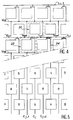
- FIG. 4 represents the elements of the elementary image points arranged on the first wall.
- These elements 20 are an a-Si: H type thin film transistor and an electrode. The drain of the transistor is connected to the electrode, while its gate is connected to a line conductor Li, and its source is brought to a reference potential Vref.
- i is a general index representing the number of the line conductor. In the figure, two consecutive line conductors Li-1 and Li have been referenced, the next line conductor Li would be referenced Li + 1. It can be seen in FIG.
- FIG. 5 represents an arrangement according to the invention of the electrodes placed on the second wall. These electrodes are arranged in columns, a column corresponding to a red R, green V or blue B color. The electrodes of the same column are connected by a column conductor Cj. j is a general index representing the number of the column conductor. In the figure, three consecutive column conductors Cj-1, Cj and Cj + 1 have been referenced.
- the arrangement of the various colored filters deposited on the electrodes makes it possible to easily produce them by an electrodeposition method.
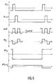
- FIG. 6 shows timing diagrams corresponding to the variations of the voltage Vref and of the voltages VLi and VLi + 1 applied to the line conductors Li and Li + 1 as well as of the voltage VCj applied to a column conductor Cj when the elementary image points corresponding to the crossings of these row conductors and this column conductor are activated.
- the addressing of the active matrices consists in successively validating the line conductors periodically, the period being called frame time T.
- the different image points corresponding to a validated line conductor and which must be activated, are activated by the control voltages VCj applied to the columns.
- the voltage applied between the electrodes of an image point corresponds to the difference VCj-Vref.
- the phase of the addressing voltage is reversed on the successive line conductors and for a given line conductor, all the frames. This means makes it possible to have an average power, dissipated in the liquid crystal, zero.
- the very structure of a thin film transistor means that a parasitic capacitor appears at the level of the gate during addressing. This parasitic element causes the appearance of a DC voltage component which disturbs the correct addressing of the image points. In order to compensate for this phenomenon, a continuous voltage ⁇ Vref is added to the reference voltage Vref.
Landscapes
- Physics & Mathematics (AREA)
- Nonlinear Science (AREA)
- Mathematical Physics (AREA)
- Chemical & Material Sciences (AREA)
- Crystallography & Structural Chemistry (AREA)
- General Physics & Mathematics (AREA)
- Optics & Photonics (AREA)
- Engineering & Computer Science (AREA)
- Microelectronics & Electronic Packaging (AREA)
- Liquid Crystal (AREA)
- Liquid Crystal Display Device Control (AREA)
- Devices For Indicating Variable Information By Combining Individual Elements (AREA)
Claims (1)
- Aktiver Matrix-Farbbildschirm ohne Kreuzung der Leiterbahnen für Adressierung und Spaltensteuerung, einen Flüssigkristall zwischen einer ersten und einer zweiten Wand angeordnet, eine Vielzahl Bildfarbpunkte, jeder Bildfarbpunkt aus den drei im Dreieck angeordneten Grundfarbpunkten Rot, Grün und Blau gebildet, jeder der Grundpunkte auf der ersten Wand bestehend aus einem Dünnfilmtransitor dessen Gate mit einer Leiterbahn für Adressierung, dessen Source mit einem einen Bezugswert (Vref) führenden Leiter, und dessen Drain mit einer Elektrode eines Kondensators verbunden ist, eine zweite Elektrode dieses Kondensators an der zweiten Wand liegend, die Elektroden der ersten Wand in Zeilen angeordnet, die Elektroden der zweiten Wand in Spalten angeordnet, jede der Elektrodenspalten entsprechend einer Farbe, nacheinander Rot (R), Grün (V), und Blau (B), und die miteinander durch einen Spaltenleiter (Cj) verbundenen Elektroden, umfassend,
dadurch gekennzeichnet, daß:
jede Zeilenleiterbahn zur Adressierung (Li) gemeinsam für zwei Zeilen aneinandergrenzender Elektroden ist, jede Leiterbahn für zwei Zeilen aneinandergrenzender Elektroden den Bezugswert (Vref) führt, man auf einer Seite einer Zeile von Elektroden, und zu diesen parallel angeordnet, eine Zeilenleiterbahn (Li), und auf der anderen Seite der Elektroden, und parallel zu diesen angeordnet, eine das Bezugspotential (Vref) führende Leiterbahn findet.
Applications Claiming Priority (2)
| Application Number | Priority Date | Filing Date | Title |
|---|---|---|---|
| FR8800200A FR2625827B1 (fr) | 1988-01-11 | 1988-01-11 | Ecran d'affichage en couleur a matrice active sans croisement des conducteurs lignes d'adressage et des conducteurs colonnes de commande |
| FR8800200 | 1988-01-11 |
Publications (2)
| Publication Number | Publication Date |
|---|---|
| EP0332476A1 EP0332476A1 (de) | 1989-09-13 |
| EP0332476B1 true EP0332476B1 (de) | 1993-05-05 |
Family
ID=9362179
Family Applications (1)
| Application Number | Title | Priority Date | Filing Date |
|---|---|---|---|
| EP89400053A Expired - Lifetime EP0332476B1 (de) | 1988-01-11 | 1989-01-09 | Aktiver Matrix-Farbbildschirm ohne Kreuzung der Leiterbahnen für Adressierung und Spaltensteuerung |
Country Status (5)
| Country | Link |
|---|---|
| US (1) | US4950058A (de) |
| EP (1) | EP0332476B1 (de) |
| JP (1) | JPH022525A (de) |
| DE (1) | DE68906295T2 (de) |
| FR (1) | FR2625827B1 (de) |
Families Citing this family (20)
| Publication number | Priority date | Publication date | Assignee | Title |
|---|---|---|---|---|
| JPH0610702B2 (ja) * | 1987-11-18 | 1994-02-09 | インターナショナル・ビジネス・マシーンズ・コーポレーション | カラー液晶表示装置およびその製造方法 |
| KR920008056B1 (ko) * | 1988-11-30 | 1992-09-22 | 주식회사 금성사 | 박막액정칼라티브이의 박막액티브매트릭스의 구조 |
| JPH0383014A (ja) * | 1989-08-28 | 1991-04-09 | Toshiba Corp | 液晶表示装置の駆動方法 |
| KR960004147B1 (ko) * | 1989-11-20 | 1996-03-27 | 쓰지 하루오 | 컬러액정표시장치 |
| JPH0484184A (ja) * | 1990-07-27 | 1992-03-17 | Nec Corp | フラット・カラー・ディスプレイパネルの画素配列方式 |
| US5076669A (en) * | 1990-12-12 | 1991-12-31 | Reliant Laser Corp. | Method and apparatus for selectively blocking light beams of different wavelengths with single color-sensitive filter |
| FR2670939B1 (fr) * | 1990-12-21 | 1996-12-20 | Thomson Lcd | Ecran matriciel couleur a filtres colores en triade. |
| JPH0742982B2 (ja) * | 1991-04-02 | 1995-05-15 | テイエチケー株式会社 | フランジ付きリニアボールベアリング |
| EP0538533A1 (de) * | 1991-10-25 | 1993-04-28 | Goldstar Co. Ltd. | Dünnfilm-Flüssigkristallmatrizen mit verbesserter Struktur |
| US5579027A (en) * | 1992-01-31 | 1996-11-26 | Canon Kabushiki Kaisha | Method of driving image display apparatus |
| JPH07114018A (ja) * | 1993-10-15 | 1995-05-02 | Rohm Co Ltd | カラー液晶表示装置 |
| US5920298A (en) * | 1996-12-19 | 1999-07-06 | Colorado Microdisplay, Inc. | Display system having common electrode modulation |
| US6046716A (en) | 1996-12-19 | 2000-04-04 | Colorado Microdisplay, Inc. | Display system having electrode modulation to alter a state of an electro-optic layer |
| US6078303A (en) * | 1996-12-19 | 2000-06-20 | Colorado Microdisplay, Inc. | Display system having electrode modulation to alter a state of an electro-optic layer |
| JP3223142B2 (ja) | 1997-08-22 | 2001-10-29 | チッソ株式会社 | 液晶表示素子の製造法 |
| JP2001154609A (ja) * | 1999-12-01 | 2001-06-08 | Kawasaki Steel Corp | 表示素子 |
| US7551189B2 (en) * | 2001-10-25 | 2009-06-23 | Hewlett-Packard Development Company, L.P. | Method of and apparatus for digital image processing |
| KR100884993B1 (ko) * | 2002-04-20 | 2009-02-20 | 엘지디스플레이 주식회사 | 액정표시장치 및 그 구동방법 |
| DE102005038100A1 (de) * | 2005-08-10 | 2007-02-15 | Micronas Gmbh | Monolithische Anordnung, insbesondere integrierte Schaltung, mit einer floatenden Elektrode |
| JP2020003600A (ja) * | 2018-06-27 | 2020-01-09 | 住友電気工業株式会社 | マッハツェンダ変調器 |
Family Cites Families (12)
| Publication number | Priority date | Publication date | Assignee | Title |
|---|---|---|---|---|
| FR2553218B1 (fr) * | 1983-10-07 | 1987-09-25 | Commissariat Energie Atomique | Ecran d'affichage a matrice active sans croisement des lignes et des colonnes d'adressage |
| JPS60188927A (ja) * | 1984-03-08 | 1985-09-26 | Toshiba Corp | カラ−・マトリツクス型液晶表示装置の製造方法 |
| JPS60218626A (ja) * | 1984-04-13 | 1985-11-01 | Sharp Corp | カラ−液晶表示装置 |
| DE3650639T2 (de) * | 1985-01-25 | 1998-02-26 | Nippon Electric Co | Aufbau eines Flüssigkristall-Mehrfarbenanzeigepaneels |
| US4678282A (en) * | 1985-02-19 | 1987-07-07 | Ovonic Imaging Systems, Inc. | Active display matrix addressable without crossed lines on any one substrate and method of using the same |
| FR2590394B1 (fr) * | 1985-11-15 | 1987-12-18 | Thomson Csf | Ecran de visualisation electro-optique a transistors de commande |
| FR2593632B1 (fr) * | 1986-01-27 | 1988-03-18 | Maurice Francois | Ecran d'affichage a matrice active et procedes de realisation de cet ecran |
| GB8604402D0 (en) * | 1986-02-21 | 1986-03-26 | Gen Electric Co Plc | Liquid crystal displays |
| NL8601063A (nl) * | 1986-04-25 | 1987-11-16 | Philips Nv | Weergeefinrichting voor kleurweergave. |
| KR900004989B1 (en) * | 1986-09-11 | 1990-07-16 | Fujitsu Ltd | Active matrix type display and driving method |
| US4822144A (en) * | 1986-12-24 | 1989-04-18 | U.S. Philips Corporation | Electro-optic color display including luminescent layer and interference filter |
| US4743099A (en) * | 1987-01-28 | 1988-05-10 | International Business Machines Corporation | Method of making a TFT LC display having polychromatic glass color filters |
-
1988
- 1988-01-11 FR FR8800200A patent/FR2625827B1/fr not_active Expired - Fee Related
-
1989
- 1989-01-05 US US07/293,638 patent/US4950058A/en not_active Expired - Fee Related
- 1989-01-09 EP EP89400053A patent/EP0332476B1/de not_active Expired - Lifetime
- 1989-01-09 DE DE89400053T patent/DE68906295T2/de not_active Expired - Fee Related
- 1989-01-10 JP JP1002165A patent/JPH022525A/ja active Pending
Also Published As
| Publication number | Publication date |
|---|---|
| DE68906295T2 (de) | 1993-10-21 |
| DE68906295D1 (de) | 1993-06-09 |
| FR2625827A1 (fr) | 1989-07-13 |
| US4950058A (en) | 1990-08-21 |
| FR2625827B1 (fr) | 1993-07-16 |
| JPH022525A (ja) | 1990-01-08 |
| EP0332476A1 (de) | 1989-09-13 |
Similar Documents
| Publication | Publication Date | Title |
|---|---|---|
| EP0332476A1 (de) | Aktiver Matrix-Farbbildschirm ohne Kreuzung der Leiterbahnen für Adressierung und Spaltensteuerung | |
| EP0145520B1 (de) | Bildschirm mit aktiver Matrix ohne Kreuzung von Zeilen- und Spaltenadressenleitungen | |
| EP0721603B1 (de) | Pixelanordnung für flachbildanzeigevorrichtung | |
| FR2625357A1 (fr) | Configuration de pixels pour obtenir une triade en couleur en quinconce | |
| FR2585167A1 (fr) | Structures conductrices redondantes pour affichages a cristaux liquides commandes par des transistors a effet de champ en couche mince | |
| FR2542119A1 (fr) | Procede pour commander un ecran d'affichage matriciel a cristaux liquides | |
| FR2767952A1 (fr) | Afficheur a cristal liquide a commutation hybride | |
| WO1994001801A1 (fr) | Dispositif de visualisation a cristaux liquides, a matrice active | |
| EP2721598B1 (de) | Flüssigkristallanzeige mit löschelektroden | |
| FR2499276A1 (fr) | Dispositif d'affichage matriciel a plusieurs jeux d'electrodes et son procede de commande | |
| EP0487389A1 (de) | Flacher Bildschirm mit aktiver Matrix | |
| FR2670939A1 (fr) | Ecran matriciel couleur a filtres colores en triade. | |
| FR2674661A1 (fr) | Structure de commande matricielle pour ecran de visualisation. | |
| JP2846351B2 (ja) | 液晶表示装置 | |
| EP0041890B1 (de) | Element mit nichtlinearer Stromführung und Schaltkreis, besonders zur Bildanzeige, mit solchem Element | |
| EP0564337A1 (de) | Anzeigeschirm mit optischer Maske und Verfahren zur Verwirklichung dieses Schirms | |
| FR2646269A1 (fr) | Cellule d'affichage electro-optique perfectionnee | |
| FR2889763A1 (fr) | Afficheur matriciel a affichage sequentiel des couleurs et procede d'adressage | |
| FR2605778A1 (fr) | Panneau de visualisation a cristaux liquides et procede d'inscription des donnees sur ce panneau | |
| JPH0150915B2 (de) | ||
| EP0692780A1 (de) | Flüssigkristallanzeigeeinrichtung mit aktiver Matrix und unterteilter Gegenelektrode | |
| EP0176384B1 (de) | Vielfarbige Matrixanzeigevorrichtung ohne Kopplung zwischen Zeilen und Spalten | |
| FR2719936A1 (fr) | Dispositif de visualisation à cristaux liquides, à matrice active. | |
| EP0607352A1 (de) | Anzeigvorrichtung mit aktiver matrix und eigebetteter masseelektrode | |
| FR2488016A1 (fr) | Module elementaire pour panneau d'affichage matriciel et panneau d'affichage comportant un tel module |
Legal Events
| Date | Code | Title | Description |
|---|---|---|---|
| PUAI | Public reference made under article 153(3) epc to a published international application that has entered the european phase |
Free format text: ORIGINAL CODE: 0009012 |
|
| AK | Designated contracting states |
Kind code of ref document: A1 Designated state(s): CH DE GB IT LI NL |
|
| 17P | Request for examination filed |
Effective date: 19900216 |
|
| 17Q | First examination report despatched |
Effective date: 19920525 |
|
| GRAA | (expected) grant |
Free format text: ORIGINAL CODE: 0009210 |
|
| AK | Designated contracting states |
Kind code of ref document: B1 Designated state(s): CH DE GB IT LI NL |
|
| REF | Corresponds to: |
Ref document number: 68906295 Country of ref document: DE Date of ref document: 19930609 |
|
| ITF | It: translation for a ep patent filed | ||
| GBT | Gb: translation of ep patent filed (gb section 77(6)(a)/1977) |
Effective date: 19930721 |
|
| PGFP | Annual fee paid to national office [announced via postgrant information from national office to epo] |
Ref country code: DE Payment date: 19940103 Year of fee payment: 6 |
|
| PGFP | Annual fee paid to national office [announced via postgrant information from national office to epo] |
Ref country code: GB Payment date: 19940105 Year of fee payment: 6 |
|
| PGFP | Annual fee paid to national office [announced via postgrant information from national office to epo] |
Ref country code: CH Payment date: 19940128 Year of fee payment: 6 |
|
| PGFP | Annual fee paid to national office [announced via postgrant information from national office to epo] |
Ref country code: NL Payment date: 19940131 Year of fee payment: 6 |
|
| PLBE | No opposition filed within time limit |
Free format text: ORIGINAL CODE: 0009261 |
|
| STAA | Information on the status of an ep patent application or granted ep patent |
Free format text: STATUS: NO OPPOSITION FILED WITHIN TIME LIMIT |
|
| 26N | No opposition filed | ||
| PG25 | Lapsed in a contracting state [announced via postgrant information from national office to epo] |
Ref country code: GB Effective date: 19950109 |
|
| PG25 | Lapsed in a contracting state [announced via postgrant information from national office to epo] |
Ref country code: LI Effective date: 19950131 Ref country code: CH Effective date: 19950131 |
|
| PG25 | Lapsed in a contracting state [announced via postgrant information from national office to epo] |
Ref country code: NL Effective date: 19950801 |
|
| GBPC | Gb: european patent ceased through non-payment of renewal fee |
Effective date: 19950109 |
|
| REG | Reference to a national code |
Ref country code: CH Ref legal event code: PL |
|
| NLV4 | Nl: lapsed or anulled due to non-payment of the annual fee |
Effective date: 19950801 |
|
| PG25 | Lapsed in a contracting state [announced via postgrant information from national office to epo] |
Ref country code: DE Effective date: 19951003 |
|
| PG25 | Lapsed in a contracting state [announced via postgrant information from national office to epo] |
Ref country code: IT Free format text: LAPSE BECAUSE OF NON-PAYMENT OF DUE FEES Effective date: 20050109 |