EP0145925B1 - Iteratives Verfahren zur Feststellung von Verbindungen zwischen Knoten und resultierendes Produkt - Google Patents
Iteratives Verfahren zur Feststellung von Verbindungen zwischen Knoten und resultierendes Produkt Download PDFInfo
- Publication number
- EP0145925B1 EP0145925B1 EP84113318A EP84113318A EP0145925B1 EP 0145925 B1 EP0145925 B1 EP 0145925B1 EP 84113318 A EP84113318 A EP 84113318A EP 84113318 A EP84113318 A EP 84113318A EP 0145925 B1 EP0145925 B1 EP 0145925B1
- Authority
- EP
- European Patent Office
- Prior art keywords
- path
- connections
- paths
- cost
- connection
- Prior art date
- Legal status (The legal status is an assumption and is not a legal conclusion. Google has not performed a legal analysis and makes no representation as to the accuracy of the status listed.)
- Expired
Links
Images


Classifications
-
- G—PHYSICS
- G06—COMPUTING OR CALCULATING; COUNTING
- G06F—ELECTRIC DIGITAL DATA PROCESSING
- G06F30/00—Computer-aided design [CAD]
- G06F30/30—Circuit design
- G06F30/39—Circuit design at the physical level
- G06F30/394—Routing
Definitions
- a mazerouter method can determine paths of various arbitrary shapes, but often requires substantial computation time but is an option provided for as disclosed hereinafter.
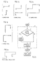
- the set of shapes to be considered is restricted to simple shapes - such as the I, L, Z, U shapes of the embodiment of the present invention disclosed hereinafter - then the other disclosed methods can be used to advantage. These methods consist of evaluating a penalty score for each of the allowed paths, and either choosing the smallest-penalty path or choosing one such path according to a probabilistic function of the penalty scores for all allowed paths. These methods can be used when the set of allowed paths is restricted and not arbitrary. The computation of a penalty function for every arbitrary path is computationally impractical or impossible.
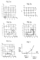
- Step 104 provides the option of starting with a specified simple path shape for the connections to be routed. If the option is elected the method proceeds to step 108, if not the method moves on to step 112. The purpose of this preparatory routing is to present the connection router with a reasonable background of wiring congestion against which each connection, in turn, will later be rerouted in an iterative fashion.
- a simple wire path shape such as an L-shaped path is chosen and the connection is oriented randomly and randomly assigned to a layer from among all the layers available.
- a detailed path penalty function F( detalled path) is defined according to user specified penalty costs. In the embodiment illustrated, these include the following costs:
- a loop including steps 436, 444, 452, 460, 468, 476 and 484 may be used in a similar manner for other applicable constraints such as a maximum allowed via count or maximum adjacency length. Multiple loops are used as required by the complexity of the routing application.
- step 500 is to calculate the diagnostics and generate data for the rerouted connection. For example, this includes the connection length in each direction in each plane, the number of vias used, the number of overloaded nodes, and a measure of crosstalk performance. Also at step 500 data is generated corresponding to the coordinates of the rerouted connection paths. At step 508 it is determined whether to exit the detailed router because the total number of passes is sufficient, or perform another pass by returning to step 324. If no further passes are required, the process stops at step 516.
Landscapes
- Engineering & Computer Science (AREA)
- Computer Hardware Design (AREA)
- Physics & Mathematics (AREA)
- Theoretical Computer Science (AREA)
- Computer Networks & Wireless Communication (AREA)
- Evolutionary Computation (AREA)
- Geometry (AREA)
- General Engineering & Computer Science (AREA)
- General Physics & Mathematics (AREA)
- Design And Manufacture Of Integrated Circuits (AREA)
Claims (19)
Applications Claiming Priority (2)
| Application Number | Priority Date | Filing Date | Title |
|---|---|---|---|
| US06/562,754 US4615011A (en) | 1983-12-19 | 1983-12-19 | Iterative method for establishing connections and resulting product |
| US562754 | 1983-12-19 |
Publications (3)
| Publication Number | Publication Date |
|---|---|
| EP0145925A2 EP0145925A2 (de) | 1985-06-26 |
| EP0145925A3 EP0145925A3 (en) | 1986-03-12 |
| EP0145925B1 true EP0145925B1 (de) | 1989-08-23 |
Family
ID=24247632
Family Applications (1)
| Application Number | Title | Priority Date | Filing Date |
|---|---|---|---|
| EP84113318A Expired EP0145925B1 (de) | 1983-12-19 | 1984-11-06 | Iteratives Verfahren zur Feststellung von Verbindungen zwischen Knoten und resultierendes Produkt |
Country Status (4)
| Country | Link |
|---|---|
| US (1) | US4615011A (de) |
| EP (1) | EP0145925B1 (de) |
| JP (1) | JPS60130843A (de) |
| DE (1) | DE3479540D1 (de) |
Families Citing this family (201)
| Publication number | Priority date | Publication date | Assignee | Title |
|---|---|---|---|---|
| JPS6156435A (ja) * | 1984-07-25 | 1986-03-22 | Fujitsu Ltd | 半導体集積回路装置に於ける配線長予測方法 |
| US5050091A (en) * | 1985-02-28 | 1991-09-17 | Electric Editor, Inc. | Integrated electric design system with automatic constraint satisfaction |
| JPS61199166A (ja) * | 1985-03-01 | 1986-09-03 | Nec Corp | 配線経路探索装置 |
| US4754408A (en) * | 1985-11-21 | 1988-06-28 | International Business Machines Corporation | Progressive insertion placement of elements on an integrated circuit |
| JPH0770598B2 (ja) * | 1986-03-20 | 1995-07-31 | 株式会社東芝 | 半導体集積回路装置の配線方法 |
| JPH0785249B2 (ja) * | 1986-05-16 | 1995-09-13 | 株式会社日立製作所 | 設計支援装置 |
| US4777606A (en) * | 1986-06-05 | 1988-10-11 | Northern Telecom Limited | Method for deriving an interconnection route between elements in an interconnection medium |
| US4858143A (en) * | 1986-09-25 | 1989-08-15 | Bell-Northern Research, Ltd. | Work ordering routine for use in a method of routing |
| JPS63225869A (ja) * | 1986-10-09 | 1988-09-20 | Nec Corp | 配線経路探索方式 |
| JPS63278249A (ja) * | 1986-12-26 | 1988-11-15 | Toshiba Corp | 半導体集積回路装置の配線方法 |
| US5021968A (en) * | 1987-01-13 | 1991-06-04 | Robertson-Ceco Corporation | Graphics-based wire-cable management system |
| US4768154A (en) * | 1987-05-08 | 1988-08-30 | Telesis Systems Corporation | Computer aided printed circuit board wiring |
| US5151984A (en) * | 1987-06-22 | 1992-09-29 | Newman William C | Block diagram simulator using a library for generation of a computer program |
| CA1300265C (en) * | 1987-06-22 | 1992-05-05 | William Curtis Newman | Block diagram simulator |
| US4852016A (en) * | 1987-06-26 | 1989-07-25 | Seattle Silicon Corporation | Moat router for integrated circuits |
| US5150309A (en) * | 1987-08-04 | 1992-09-22 | Texas Instruments Incorporated | Comprehensive logic circuit layout system |
| US4870598A (en) * | 1987-08-04 | 1989-09-26 | Texas Instruments Incorporated | Comprehensive logic circuit layout system |
| US5684723A (en) * | 1987-11-16 | 1997-11-04 | Fujitsu Limited | Device simulation method and device simulator |
| JP2535976B2 (ja) * | 1987-11-17 | 1996-09-18 | 株式会社日立製作所 | 形態接続構成自動作成システム |
| JP2690929B2 (ja) * | 1988-02-26 | 1997-12-17 | 株式会社日立製作所 | Mosトランジスタ間の配線方法 |
| US5119317A (en) * | 1988-03-16 | 1992-06-02 | Kabushiki Kaisha Toshiba | Routing method and system |
| US4970664A (en) * | 1988-06-10 | 1990-11-13 | Kaiser Richard R | Critical path analyzer with path context window |
| US4831725A (en) * | 1988-06-10 | 1989-05-23 | International Business Machines Corporation | Global wiring by removal of redundant paths |
| US4953094A (en) * | 1988-07-01 | 1990-08-28 | Aerohydro, Inc. | Method for lofting blanks and compounding plates for shell structures |
| US5047959A (en) * | 1988-09-13 | 1991-09-10 | Square D Company | Flexible data display |
| DE3935418A1 (de) * | 1988-10-24 | 1990-04-26 | Hitachi Ltd | Verfahren und vorrichtung zur bestimmung von verdrahtungsmustern |
| US5159682A (en) * | 1988-10-28 | 1992-10-27 | Matsushita Electric Industrial Co., Ltd. | System for optimizing a physical organization of elements of an integrated circuit chip through the convergence of a redundancy function |
| US5032991A (en) * | 1988-12-14 | 1991-07-16 | At&T Ball Laboratories | Method for routing conductive paths |
| JPH02206149A (ja) * | 1989-02-06 | 1990-08-15 | Hitachi Ltd | 電気的制約を考慮した信号線端子割付方式 |
| US5351197A (en) * | 1989-04-13 | 1994-09-27 | Cascade Design Automation Corporation | Method and apparatus for designing the layout of a subcircuit in an integrated circuit |
| US5072379A (en) * | 1989-05-26 | 1991-12-10 | The United States Of America As Represented By The Adminstrator Of The National Aeronautics And Space Administration | Network of dedicated processors for finding lowest-cost map path |
| US5309371A (en) * | 1989-06-28 | 1994-05-03 | Kawasaki Steel Corporation | Method of and apparatus for designing circuit block layout in integrated circuit |
| EP0431532B1 (de) * | 1989-12-04 | 2001-04-18 | Matsushita Electric Industrial Co., Ltd. | Plazierungsoptimierungssystem mit Hilfe von CAD |
| JP3032224B2 (ja) * | 1990-02-21 | 2000-04-10 | 株式会社東芝 | 半導体集積回路の論理セル配置方法 |
| US5367469A (en) * | 1990-12-13 | 1994-11-22 | Vlsi Technology, Inc. | Predictive capacitance layout method for integrated circuits |
| US5309370A (en) * | 1990-12-13 | 1994-05-03 | Vlsi Technology, Inc. | Method for placement of connectors used interconnecting circuit components in an integrated circuit |
| US5237514A (en) * | 1990-12-21 | 1993-08-17 | International Business Machines Corporation | Minimizing path delay in a machine by compensation of timing through selective placement and partitioning |
| US5341310A (en) * | 1991-12-17 | 1994-08-23 | International Business Machines Corporation | Wiring layout design method and system for integrated circuits |
| JP2759573B2 (ja) * | 1992-01-23 | 1998-05-28 | 株式会社日立製作所 | 回路基板の配線パターン決定方法 |
| US5353235A (en) * | 1992-06-17 | 1994-10-04 | Vlsi Technology, Inc. | Wire length minimization in channel compactor |
| US5493510A (en) * | 1992-11-10 | 1996-02-20 | Kawasaki Steel Corporation | Method of and apparatus for placing blocks in semiconductor integrated circuit |
| US5729469A (en) * | 1992-12-07 | 1998-03-17 | Matsushita Electric Industrial Co., Ltd. | Wiring method and system for integrated circuit |
| CA2102855A1 (en) * | 1992-12-29 | 1994-06-30 | Albon E. Gilbert | Jumper cable selection and routing system |
| US5519632A (en) * | 1993-04-05 | 1996-05-21 | International Business Machines Corporation | Automatic DCS routing for multilayer packages to minimize coupled noise |
| US5360767A (en) * | 1993-04-12 | 1994-11-01 | International Business Machines Corporation | Method for assigning pins to connection points |
| JPH07152802A (ja) * | 1993-12-01 | 1995-06-16 | Nec Corp | 配線設計方法 |
| US5471397A (en) * | 1993-12-15 | 1995-11-28 | International Business Machines Corporation | Identifying subsets of noise violators and contributors in package wiring |
| US5875117A (en) * | 1994-04-19 | 1999-02-23 | Lsi Logic Corporation | Simultaneous placement and routing (SPAR) method for integrated circuit physical design automation system |
| US5914887A (en) * | 1994-04-19 | 1999-06-22 | Lsi Logic Corporation | Congestion based cost factor computing apparatus for integrated circuit physical design automation system |
| US5495419A (en) * | 1994-04-19 | 1996-02-27 | Lsi Logic Corporation | Integrated circuit physical design automation system utilizing optimization process decomposition and parallel processing |
| US6493658B1 (en) | 1994-04-19 | 2002-12-10 | Lsi Logic Corporation | Optimization processing for integrated circuit physical design automation system using optimally switched fitness improvement algorithms |
| US6155725A (en) * | 1994-04-19 | 2000-12-05 | Lsi Logic Corporation | Cell placement representation and transposition for integrated circuit physical design automation system |
| US5963975A (en) * | 1994-04-19 | 1999-10-05 | Lsi Logic Corporation | Single chip integrated circuit distributed shared memory (DSM) and communications nodes |
| US5815403A (en) * | 1994-04-19 | 1998-09-29 | Lsi Logic Corporation | Fail-safe distributive processing method for producing a highest fitness cell placement for an integrated circuit chip |
| US5557533A (en) * | 1994-04-19 | 1996-09-17 | Lsi Logic Corporation | Cell placement alteration apparatus for integrated circuit chip physical design automation system |
| JP3571369B2 (ja) * | 1994-06-16 | 2004-09-29 | 富士通株式会社 | 配線設計装置 |
| US5523960A (en) * | 1994-08-10 | 1996-06-04 | Samsung Electronics Co., Ltd. | Evaluation method of assembly sequences |
| US5638288A (en) * | 1994-08-24 | 1997-06-10 | Lsi Logic Corporation | Separable cells having wiring channels for routing signals between surrounding cells |
| US5587923A (en) * | 1994-09-07 | 1996-12-24 | Lsi Logic Corporation | Method for estimating routability and congestion in a cell placement for integrated circuit chip |
| US5701255A (en) * | 1994-09-14 | 1997-12-23 | Matsushita Electric Industrial Co., Ltd. | Cell generation method and cell generation system |
| US6058252A (en) * | 1995-01-19 | 2000-05-02 | Synopsys, Inc. | System and method for generating effective layout constraints for a circuit design or the like |
| AU4866596A (en) * | 1995-02-07 | 1996-08-27 | Silicon Valley Research, Inc. | Integrated circuit layout |
| US5841664A (en) * | 1996-03-12 | 1998-11-24 | Avant| Corporation | Method for optimizing track assignment in a grid-based channel router |
| AU2327997A (en) | 1996-03-15 | 1997-10-01 | University Of Arizona, The | Interconnection routing system |
| US6026223A (en) * | 1996-06-28 | 2000-02-15 | Scepanovic; Ranko | Advanced modular cell placement system with overlap remover with minimal noise |
| US6085032A (en) * | 1996-06-28 | 2000-07-04 | Lsi Logic Corporation | Advanced modular cell placement system with sinusoidal optimization |
| US5963455A (en) * | 1996-06-28 | 1999-10-05 | Lsi Logic Corporation | Advanced modular cell placement system with functional sieve optimization technique |
| US5892688A (en) * | 1996-06-28 | 1999-04-06 | Lsi Logic Corporation | Advanced modular cell placement system with iterative one dimensional preplacement optimization |
| US5831863A (en) * | 1996-06-28 | 1998-11-03 | Lsi Logic Corporation | Advanced modular cell placement system with wire length driven affinity system |
| US5867398A (en) * | 1996-06-28 | 1999-02-02 | Lsi Logic Corporation | Advanced modular cell placement system with density driven capacity penalty system |
| US5870311A (en) * | 1996-06-28 | 1999-02-09 | Lsi Logic Corporation | Advanced modular cell placement system with fast procedure for finding a levelizing cut point |
| US5870312A (en) * | 1996-06-28 | 1999-02-09 | Lsi Logic Corporation | Advanced modular cell placement system with dispersion-driven levelizing system |
| US6067409A (en) * | 1996-06-28 | 2000-05-23 | Lsi Logic Corporation | Advanced modular cell placement system |
| US5808899A (en) * | 1996-06-28 | 1998-09-15 | Lsi Logic Corporation | Advanced modular cell placement system with cell placement crystallization |
| US5844811A (en) * | 1996-06-28 | 1998-12-01 | Lsi Logic Corporation | Advanced modular cell placement system with universal affinity driven discrete placement optimization |
| US5812740A (en) * | 1996-06-28 | 1998-09-22 | Lsi Logic Corporation | Advanced modular cell placement system with neighborhood system driven optimization |
| US5835381A (en) * | 1996-06-28 | 1998-11-10 | Lsi Logic Corporation | Advanced modular cell placement system with minimizing maximal cut driven affinity system |
| US5914888A (en) * | 1996-06-28 | 1999-06-22 | Lsi Logic Corporation | Advanced modular cell placement system with coarse overflow remover |
| US5872718A (en) * | 1996-06-28 | 1999-02-16 | Lsi Logic Corporation | Advanced modular cell placement system |
| US6030110A (en) * | 1996-06-28 | 2000-02-29 | Lsi Logic Corporation | Advanced modular cell placement system with median control and increase in resolution |
| US5963728A (en) * | 1996-08-14 | 1999-10-05 | International Business Machines Corporation | Method to partition clock sinks into nets |
| US5980093A (en) * | 1996-12-04 | 1999-11-09 | Lsi Logic Corporation | Integrated circuit layout routing using multiprocessing |
| US6330707B1 (en) * | 1997-09-29 | 2001-12-11 | Matsushita Electric Industrial Co., Ltd. | Automatic routing method |
| US6266802B1 (en) * | 1997-10-27 | 2001-07-24 | International Business Machines Corporation | Detailed grid point layout using a massively parallel logic including an emulator/simulator paradigm |
| JP3178399B2 (ja) * | 1997-12-04 | 2001-06-18 | 日本電気株式会社 | 半導体集積回路、その素子配置方法およびその製造方法 |
| US6230304B1 (en) | 1997-12-24 | 2001-05-08 | Magma Design Automation, Inc. | Method of designing a constraint-driven integrated circuit layout |
| JP3530025B2 (ja) * | 1998-06-16 | 2004-05-24 | 富士通株式会社 | 概略配線決定方法及び記憶媒体 |
| US6182272B1 (en) * | 1998-07-16 | 2001-01-30 | Lsi Logic Corporation | Metal layer assignment |
| US6279142B1 (en) | 1998-10-02 | 2001-08-21 | International Business Machines Corporation | Method of on-chip interconnect design |
| US6263480B1 (en) * | 1998-12-30 | 2001-07-17 | International Business Machines Corporation | Efficient tracing of shorts in very large nets in hierarchical designs |
| US6507941B1 (en) * | 1999-04-28 | 2003-01-14 | Magma Design Automation, Inc. | Subgrid detailed routing |
| US6305004B1 (en) * | 1999-08-31 | 2001-10-16 | International Business Machines Corporation | Method for improving wiring related yield and capacitance properties of integrated circuits by maze-routing |
| US6519751B2 (en) * | 2000-03-31 | 2003-02-11 | Intel Corporation | Method and apparatus for accurate crosspoint allocation in VLSI area routing |
| JP2001291771A (ja) * | 2000-04-04 | 2001-10-19 | Mitsubishi Electric Corp | 自動配置配線装置及び自動配置配線方法 |
| US6889372B1 (en) | 2000-07-15 | 2005-05-03 | Cadence Design Systems Inc. | Method and apparatus for routing |
| US6898773B1 (en) * | 2002-01-22 | 2005-05-24 | Cadence Design Systems, Inc. | Method and apparatus for producing multi-layer topological routes |
| US6601222B1 (en) * | 2000-10-13 | 2003-07-29 | International Business Machines Corporation | Coupled noise estimation and avoidance of noise-failure using global routing information |
| US7055120B2 (en) * | 2000-12-06 | 2006-05-30 | Cadence Design Systems, Inc. | Method and apparatus for placing circuit modules |
| US7003754B2 (en) | 2000-12-07 | 2006-02-21 | Cadence Design Systems, Inc. | Routing method and apparatus that use of diagonal routes |
| AU2002233977A1 (en) * | 2000-12-06 | 2002-06-18 | Simplex Solutions, Inc. | Method and apparatus for considering diagonal wiring in placement |
| US6826737B2 (en) | 2000-12-06 | 2004-11-30 | Cadence Design Systems, Inc. | Recursive partitioning placement method and apparatus |
| US7080336B2 (en) * | 2000-12-06 | 2006-07-18 | Cadence Design Systems, Inc. | Method and apparatus for computing placement costs |
| US6516455B1 (en) * | 2000-12-06 | 2003-02-04 | Cadence Design Systems, Inc. | Partitioning placement method using diagonal cutlines |
| US6957410B2 (en) * | 2000-12-07 | 2005-10-18 | Cadence Design Systems, Inc. | Method and apparatus for adaptively selecting the wiring model for a design region |
| US7024650B2 (en) * | 2000-12-06 | 2006-04-04 | Cadence Design Systems, Inc. | Method and apparatus for considering diagonal wiring in placement |
| US7073150B2 (en) * | 2000-12-07 | 2006-07-04 | Cadence Design Systems, Inc. | Hierarchical routing method and apparatus that use diagonal routes |
| US7441220B2 (en) * | 2000-12-07 | 2008-10-21 | Cadence Design Systems, Inc. | Local preferred direction architecture, tools, and apparatus |
| US7594196B2 (en) * | 2000-12-07 | 2009-09-22 | Cadence Design Systems, Inc. | Block interstitching using local preferred direction architectures, tools, and apparatus |
| US6536027B1 (en) * | 2000-12-13 | 2003-03-18 | Lsi Logic Corporation | Cell pin extensions for integrated circuits |
| US7096448B2 (en) | 2001-01-19 | 2006-08-22 | Cadence Design Systems, Inc. | Method and apparatus for diagonal routing by using several sets of lines |
| US6915501B2 (en) | 2001-01-19 | 2005-07-05 | Cadence Design Systems, Inc. | LP method and apparatus for identifying routes |
| US6957411B1 (en) | 2001-06-03 | 2005-10-18 | Cadence Design Systems, Inc. | Gridless IC layout and method and apparatus for generating such a layout |
| US6829757B1 (en) | 2001-06-03 | 2004-12-07 | Cadence Design Systems, Inc. | Method and apparatus for generating multi-layer routes |
| US7310793B1 (en) | 2001-06-03 | 2007-12-18 | Cadence Design Systems, Inc. | Interconnect lines with non-rectilinear terminations |
| US7069530B1 (en) | 2001-06-03 | 2006-06-27 | Cadence Design Systems, Inc. | Method and apparatus for routing groups of paths |
| US6882055B1 (en) | 2001-06-03 | 2005-04-19 | Cadence Design Systems, Inc. | Non-rectilinear polygonal vias |
| US7107564B1 (en) * | 2001-06-03 | 2006-09-12 | Cadence Design Systems, Inc. | Method and apparatus for routing a set of nets |
| US6895569B1 (en) | 2001-06-03 | 2005-05-17 | Candence Design Systems, Inc. | IC layout with non-quadrilateral Steiner points |
| US6859916B1 (en) | 2001-06-03 | 2005-02-22 | Cadence Design Systems, Inc. | Polygonal vias |
| US6976238B1 (en) | 2001-06-03 | 2005-12-13 | Cadence Design Systems, Inc. | Circular vias and interconnect-line ends |
| US6957408B1 (en) | 2002-01-22 | 2005-10-18 | Cadence Design Systems, Inc. | Method and apparatus for routing nets in an integrated circuit layout |
| US6877146B1 (en) | 2001-06-03 | 2005-04-05 | Cadence Design Systems, Inc. | Method and apparatus for routing a set of nets |
| JP2003030266A (ja) * | 2001-07-12 | 2003-01-31 | Hitachi Ltd | 半導体集積回路の配線経路設定方法 |
| US6745379B2 (en) | 2001-08-23 | 2004-06-01 | Cadence Design Systems, Inc. | Method and apparatus for identifying propagation for routes with diagonal edges |
| US7143382B2 (en) | 2001-08-23 | 2006-11-28 | Cadence Design Systems, Inc. | Method and apparatus for storing routes |
| US6931616B2 (en) * | 2001-08-23 | 2005-08-16 | Cadence Design Systems, Inc. | Routing method and apparatus |
| US7398498B2 (en) | 2001-08-23 | 2008-07-08 | Cadence Design Systems, Inc. | Method and apparatus for storing routes for groups of related net configurations |
| US6795958B2 (en) * | 2001-08-23 | 2004-09-21 | Cadence Design Systems, Inc. | Method and apparatus for generating routes for groups of related node configurations |
| US6678876B2 (en) * | 2001-08-24 | 2004-01-13 | Formfactor, Inc. | Process and apparatus for finding paths through a routing space |
| US7058913B1 (en) | 2001-09-06 | 2006-06-06 | Cadence Design Systems, Inc. | Analytical placement method and apparatus |
| US7444269B2 (en) * | 2001-09-29 | 2008-10-28 | The Boeing Company | Constraint-based method of designing a route for a transport element |
| US7668700B2 (en) * | 2001-09-29 | 2010-02-23 | The Boeing Company | Adaptive distance field constraint for designing a route for a transport element |
| US6694502B2 (en) | 2001-11-02 | 2004-02-17 | Sun Microsystems, Inc. | Data structure for fine-grid multi-level VLSI routing and method for storing the data structure in a computer readable medium |
| US7013451B1 (en) | 2002-01-22 | 2006-03-14 | Cadence Design Systems, Inc. | Method and apparatus for performing routability checking |
| US6938234B1 (en) | 2002-01-22 | 2005-08-30 | Cadence Design Systems, Inc. | Method and apparatus for defining vias |
| US6944841B1 (en) | 2002-01-22 | 2005-09-13 | Cadence Design Systems, Inc. | Method and apparatus for proportionate costing of vias |
| US7096449B1 (en) | 2002-01-22 | 2006-08-22 | Cadence Design Systems, Inc. | Layouts with routes with different widths in different directions on the same layer, and method and apparatus for generating such layouts |
| US7080329B1 (en) | 2002-01-22 | 2006-07-18 | Cadence Design Systems, Inc. | Method and apparatus for identifying optimized via locations |
| US6892371B1 (en) | 2002-01-22 | 2005-05-10 | Cadence Design Systems, Inc. | Method and apparatus for performing geometric routing |
| US7117468B1 (en) | 2002-01-22 | 2006-10-03 | Cadence Design Systems, Inc. | Layouts with routes with different spacings in different directions on the same layer, and method and apparatus for generating such layouts |
| US7089524B1 (en) | 2002-01-22 | 2006-08-08 | Cadence Design Systems, Inc. | Topological vias route wherein the topological via does not have a coordinate within the region |
| US7036105B1 (en) | 2002-01-22 | 2006-04-25 | Cadence Design Systems, Inc. | Integrated circuits with at least one layer that has more than one preferred interconnect direction, and method for manufacturing such IC's |
| US6769108B2 (en) * | 2002-03-14 | 2004-07-27 | International Business Machines Corporation | Triangular assignment of pins used for diagonal interconnections between diagonal chips in a multi-chip module |
| US7073151B1 (en) * | 2002-06-04 | 2006-07-04 | Cadence Design Systems, Inc. | Method and apparatus for identifying a path between a set of source states and a set of target states in a triangulated space |
| US6986117B1 (en) * | 2002-06-04 | 2006-01-10 | Cadence Design Systems, Inc. | Method and apparatus for identifying a path between source and target states |
| US8675493B2 (en) * | 2002-07-02 | 2014-03-18 | Alcatel Lucent | Routing bandwidth guaranteed paths with local restoration in label switched networks |
| US20040044979A1 (en) | 2002-08-27 | 2004-03-04 | Aji Sandeep A. | Constraint-based global router for routing high performance designs |
| US7003752B2 (en) * | 2002-11-18 | 2006-02-21 | Cadence Design Systems, Inc. | Method and apparatus for routing |
| US7093221B2 (en) * | 2002-11-18 | 2006-08-15 | Cadence Design Systems, Inc. | Method and apparatus for identifying a group of routes for a set of nets |
| US6996789B2 (en) * | 2002-11-18 | 2006-02-07 | Cadence Design Systems, Inc. | Method and apparatus for performing an exponential path search |
| US7480885B2 (en) | 2002-11-18 | 2009-01-20 | Cadence Design Systems, Inc. | Method and apparatus for routing with independent goals on different layers |
| US6892369B2 (en) * | 2002-11-18 | 2005-05-10 | Cadence Design Systems, Inc. | Method and apparatus for costing routes of nets |
| US6988257B2 (en) * | 2002-11-18 | 2006-01-17 | Cadence Design Systems, Inc. | Method and apparatus for routing |
| US7047513B2 (en) * | 2002-11-18 | 2006-05-16 | Cadence Design Systems, Inc. | Method and apparatus for searching for a three-dimensional global path |
| US7010771B2 (en) * | 2002-11-18 | 2006-03-07 | Cadence Design Systems, Inc. | Method and apparatus for searching for a global path |
| US7624367B2 (en) | 2002-11-18 | 2009-11-24 | Cadence Design Systems, Inc. | Method and system for routing |
| US7171635B2 (en) * | 2002-11-18 | 2007-01-30 | Cadence Design Systems, Inc. | Method and apparatus for routing |
| US7216308B2 (en) * | 2002-11-18 | 2007-05-08 | Cadence Design Systems, Inc. | Method and apparatus for solving an optimization problem in an integrated circuit layout |
| US7080342B2 (en) * | 2002-11-18 | 2006-07-18 | Cadence Design Systems, Inc | Method and apparatus for computing capacity of a region for non-Manhattan routing |
| US7089519B1 (en) | 2002-12-31 | 2006-08-08 | Cadence Design System, Inc. | Method and system for performing placement on non Manhattan semiconductor integrated circuits |
| US7506295B1 (en) | 2002-12-31 | 2009-03-17 | Cadence Design Systems, Inc. | Non manhattan floor plan architecture for integrated circuits |
| US7013445B1 (en) | 2002-12-31 | 2006-03-14 | Cadence Design Systems, Inc. | Post processor for optimizing manhattan integrated circuits placements into non manhattan placements |
| US20040267977A1 (en) * | 2003-06-30 | 2004-12-30 | Mysore Sriram | Topology based replacement routing of signal paths |
| US7131096B1 (en) | 2004-06-01 | 2006-10-31 | Pulsic Limited | Method of automatically routing nets according to current density rules |
| US8095903B2 (en) * | 2004-06-01 | 2012-01-10 | Pulsic Limited | Automatically routing nets with variable spacing |
| US7373628B1 (en) | 2004-06-01 | 2008-05-13 | Pulsic Limited | Method of automatically routing nets using a Steiner tree |
| US7784010B1 (en) | 2004-06-01 | 2010-08-24 | Pulsic Limited | Automatic routing system with variable width interconnect |
| US7340711B2 (en) * | 2004-06-04 | 2008-03-04 | Cadence Design Systems, Inc. | Method and apparatus for local preferred direction routing |
| US7707537B2 (en) * | 2004-06-04 | 2010-04-27 | Cadence Design Systems, Inc. | Method and apparatus for generating layout regions with local preferred directions |
| US7412682B2 (en) * | 2004-06-04 | 2008-08-12 | Cadence Design Systems, Inc | Local preferred direction routing |
| US7257797B1 (en) | 2004-06-07 | 2007-08-14 | Pulsic Limited | Method of automatic shape-based routing of interconnects in spines for integrated circuit design |
| US7168053B1 (en) | 2004-12-29 | 2007-01-23 | Cadence Design Systems, Inc. | Method and system for implementing an analytical wirelength formulation |
| US7107556B1 (en) * | 2004-12-29 | 2006-09-12 | Cadence Design Systems, Inc. | Method and system for implementing an analytical wirelength formulation for unavailability of routing directions |
| US7188322B2 (en) * | 2005-02-25 | 2007-03-06 | International Business Machines Corporation | Circuit layout methodology using a shape processing application |
| US7308669B2 (en) * | 2005-05-18 | 2007-12-11 | International Business Machines Corporation | Use of redundant routes to increase the yield and reliability of a VLSI layout |
| US20060281221A1 (en) * | 2005-06-09 | 2006-12-14 | Sharad Mehrotra | Enhanced routing grid system and method |
| US9245082B2 (en) | 2005-06-21 | 2016-01-26 | Pulsic Limited | High-speed shape-based router |
| US7603644B2 (en) | 2005-06-24 | 2009-10-13 | Pulsic Limited | Integrated circuit routing and compaction |
| US7614024B2 (en) * | 2005-10-06 | 2009-11-03 | Broadcom Corporation | Method to implement metal fill during integrated circuit design and layout |
| US7363607B2 (en) * | 2005-11-08 | 2008-04-22 | Pulsic Limited | Method of automatically routing nets according to parasitic constraint rules |
| US7512907B2 (en) * | 2006-02-01 | 2009-03-31 | International Business Machines Corporation | Generating rules for nets that cross package boundaries |
| US8250514B1 (en) | 2006-07-13 | 2012-08-21 | Cadence Design Systems, Inc. | Localized routing direction |
| US7562330B1 (en) | 2006-11-06 | 2009-07-14 | Cadence Design Systems, Inc. | Budgeting global constraints on local constraints in an autorouter |
| US8458636B1 (en) | 2009-03-18 | 2013-06-04 | Pulsic Limited | Filling vacant areas of an integrated circuit design |
| US9940421B1 (en) | 2010-10-11 | 2018-04-10 | Pulsic Limited | Method for optimizing place-and-routing using a random normalized polish expression |
| US8683416B1 (en) * | 2011-07-28 | 2014-03-25 | Juniper Networks, Inc. | Integrated circuit optimization |
| US8930008B2 (en) * | 2012-01-26 | 2015-01-06 | Sakti3, Inc. | Methodology for design of a manufacturing facility for fabrication of solid state hybrid thin film energy storage and conversion devices |
| US8635577B2 (en) * | 2012-06-01 | 2014-01-21 | International Business Machines Corporation | Timing refinement re-routing |
| US9325483B2 (en) | 2013-03-15 | 2016-04-26 | Wi-Lan Labs, Inc. | Flexible MIMO resource allocation through cross-correlation nulling and frequency domain segmented receiver processing |
| US9326183B2 (en) | 2013-03-15 | 2016-04-26 | Wi-Lan Labs, Inc. | Uplink interference resolution in a wireless communication system |
| TWI643082B (zh) * | 2013-09-03 | 2018-12-01 | 美商新思科技股份有限公司 | 一種佈線出一解決路徑之方法及系統 |
| US8930873B1 (en) * | 2013-11-15 | 2015-01-06 | International Business Machines Corporation | Creating regional routing blockages in integrated circuit design |
| US10409934B1 (en) * | 2014-01-30 | 2019-09-10 | Cadence Design Systems, Inc. | System, method, and computer program product for static and dynamic phase matching in an electronic circuit design |
| US10069546B2 (en) * | 2015-02-13 | 2018-09-04 | Taiwan Semiconductor Manufacturing Co., Ltd. | Enhanced pre-ordered pre-weighted transmission |
| US9780854B2 (en) | 2015-03-30 | 2017-10-03 | Taiwan Semiconductor Manufacturing Co., Ltd. | Multi-layer wireless streaming with adaptive constellation mapping (ACM) |
| US10650621B1 (en) | 2016-09-13 | 2020-05-12 | Iocurrents, Inc. | Interfacing with a vehicular controller area network |
| JP1793996S (ja) * | 2023-05-31 | 2025-03-21 | 座標指示用画像 | |
| JP1793298S (ja) * | 2023-05-31 | 2025-03-12 | プレイエリア設定用画像 | |
| JP1765501S (ja) * | 2023-05-31 | 2024-03-13 | プレイエリア表示用画像 | |
| JP1765505S (ja) * | 2023-05-31 | 2024-03-13 | プレイエリア表示用画像 | |
| JP1765502S (ja) * | 2023-05-31 | 2024-03-13 | プレイエリア設定用画像 |
Family Cites Families (7)
| Publication number | Priority date | Publication date | Assignee | Title |
|---|---|---|---|---|
| FR1502554A (de) * | 1965-12-01 | 1968-02-07 | ||
| US3603771A (en) * | 1969-07-15 | 1971-09-07 | Texas Instruments Inc | Input/output signal point assignment |
| US3653072A (en) * | 1970-01-08 | 1972-03-28 | Texas Instruments Inc | Process for producing circuit artwork utilizing a data processing machine |
| US3653071A (en) * | 1970-01-08 | 1972-03-28 | Texas Instruments Inc | Process for producing circuit artwork utilizing a data processing machine |
| US3681782A (en) * | 1970-12-02 | 1972-08-01 | Honeywell Inf Systems | Machine process for positioning interconnected components to minimize interconnecting line length |
| DE2445368A1 (de) * | 1974-09-23 | 1976-04-01 | Siemens Ag | Verfahren zur herstellung fuer maskenvorlagen fuer integrierte halbleiterschaltungen |
| US4495559A (en) * | 1981-11-02 | 1985-01-22 | International Business Machines Corporation | Optimization of an organization of many discrete elements |
-
1983
- 1983-12-19 US US06/562,754 patent/US4615011A/en not_active Expired - Fee Related
-
1984
- 1984-07-20 JP JP59149847A patent/JPS60130843A/ja active Pending
- 1984-11-06 DE DE8484113318T patent/DE3479540D1/de not_active Expired
- 1984-11-06 EP EP84113318A patent/EP0145925B1/de not_active Expired
Also Published As
| Publication number | Publication date |
|---|---|
| EP0145925A3 (en) | 1986-03-12 |
| US4615011A (en) | 1986-09-30 |
| JPS60130843A (ja) | 1985-07-12 |
| DE3479540D1 (en) | 1989-09-28 |
| EP0145925A2 (de) | 1985-06-26 |
Similar Documents
| Publication | Publication Date | Title |
|---|---|---|
| US4615011A (en) | Iterative method for establishing connections and resulting product | |
| US5657242A (en) | Method of determining routes for a plurality of wiring connections and a circuit board produced by such a method | |
| US5644500A (en) | Routing program generating method and apparatus therefor, placement program generating method and apparatus therefor, and automatic routing method and apparatus therefor | |
| US5295082A (en) | Efficient method for multichip module interconnect | |
| US6002857A (en) | Symbolic constraint-based system for preroute reconstruction following floorplan incrementing | |
| JP3063828B2 (ja) | 集積回路の自動概略配線方法 | |
| KR0153392B1 (ko) | Lsi용 상호접속 배선 설계 방법 | |
| US20240119214A1 (en) | Using a machine trained network during routing to account for opc cost | |
| US20030009737A1 (en) | Detailed method for routing connections using tile expansion techniques and associated methods for designing and manufacturing VLSI circuits | |
| JPH077427B2 (ja) | ノードの相互接続方法 | |
| WO2000065489A1 (en) | Subgrid detailed routing | |
| US6532581B1 (en) | Method for designing layout of semiconductor device, storage medium having stored thereon program for executing the layout designing method, and semiconductor device | |
| Linsker | An iterative-improvement penalty-function-driven wire routing system | |
| US20180285508A1 (en) | Capacity model for global routing | |
| US6615399B2 (en) | Semiconductor device having dummy pattern | |
| US20010011362A1 (en) | Semiconductor layout design method and apparatus | |
| JP4803997B2 (ja) | 半導体集積装置、その設計方法、設計装置、およびプログラム | |
| US8250514B1 (en) | Localized routing direction | |
| JP5380969B2 (ja) | レイアウト設計方法、及び装置 | |
| US5825659A (en) | Method for local rip-up and reroute of signal paths in an IC design | |
| JP5900540B2 (ja) | レイアウト設計方法及びレイアウト設計支援プログラム | |
| JP3068892B2 (ja) | 自動配線方法 | |
| US20180285507A1 (en) | Engineering change order aware global routing | |
| JP3548398B2 (ja) | 概略経路決定方法および概略経路決定方式 | |
| JPH10144798A (ja) | グリッド化ポートのための自動レイアウトワイヤ最小化 |
Legal Events
| Date | Code | Title | Description |
|---|---|---|---|
| PUAI | Public reference made under article 153(3) epc to a published international application that has entered the european phase |
Free format text: ORIGINAL CODE: 0009012 |
|
| 17P | Request for examination filed |
Effective date: 19841214 |
|
| AK | Designated contracting states |
Designated state(s): DE FR GB |
|
| PUAL | Search report despatched |
Free format text: ORIGINAL CODE: 0009013 |
|
| AK | Designated contracting states |
Kind code of ref document: A3 Designated state(s): DE FR GB |
|
| 17Q | First examination report despatched |
Effective date: 19880304 |
|
| GRAA | (expected) grant |
Free format text: ORIGINAL CODE: 0009210 |
|
| AK | Designated contracting states |
Kind code of ref document: B1 Designated state(s): DE FR GB |
|
| REF | Corresponds to: |
Ref document number: 3479540 Country of ref document: DE Date of ref document: 19890928 |
|
| ET | Fr: translation filed | ||
| PLBE | No opposition filed within time limit |
Free format text: ORIGINAL CODE: 0009261 |
|
| STAA | Information on the status of an ep patent application or granted ep patent |
Free format text: STATUS: NO OPPOSITION FILED WITHIN TIME LIMIT |
|
| 26N | No opposition filed | ||
| PGFP | Annual fee paid to national office [announced via postgrant information from national office to epo] |
Ref country code: GB Payment date: 19951024 Year of fee payment: 12 |
|
| PGFP | Annual fee paid to national office [announced via postgrant information from national office to epo] |
Ref country code: FR Payment date: 19951107 Year of fee payment: 12 |
|
| PGFP | Annual fee paid to national office [announced via postgrant information from national office to epo] |
Ref country code: DE Payment date: 19951123 Year of fee payment: 12 |
|
| PG25 | Lapsed in a contracting state [announced via postgrant information from national office to epo] |
Ref country code: GB Effective date: 19961106 |
|
| GBPC | Gb: european patent ceased through non-payment of renewal fee |
Effective date: 19961106 |
|
| PG25 | Lapsed in a contracting state [announced via postgrant information from national office to epo] |
Ref country code: FR Effective date: 19970731 |
|
| PG25 | Lapsed in a contracting state [announced via postgrant information from national office to epo] |
Ref country code: DE Effective date: 19970801 |
|
| REG | Reference to a national code |
Ref country code: FR Ref legal event code: ST |