EP0146796A2 - Verfahren zur Herstellung von Dünnfilmmagnetkopfspalten durch Wegätzen - Google Patents
Verfahren zur Herstellung von Dünnfilmmagnetkopfspalten durch Wegätzen Download PDFInfo
- Publication number
- EP0146796A2 EP0146796A2 EP84114282A EP84114282A EP0146796A2 EP 0146796 A2 EP0146796 A2 EP 0146796A2 EP 84114282 A EP84114282 A EP 84114282A EP 84114282 A EP84114282 A EP 84114282A EP 0146796 A2 EP0146796 A2 EP 0146796A2
- Authority
- EP
- European Patent Office
- Prior art keywords
- lift
- solution
- copper
- gap
- metallization layer
- Prior art date
- Legal status (The legal status is an assumption and is not a legal conclusion. Google has not performed a legal analysis and makes no representation as to the accuracy of the status listed.)
- Withdrawn
Links
- 238000000034 method Methods 0.000 title claims abstract description 34
- 239000010409 thin film Substances 0.000 title claims abstract description 14
- 238000004519 manufacturing process Methods 0.000 title claims abstract description 12
- RYGMFSIKBFXOCR-UHFFFAOYSA-N Copper Chemical compound [Cu] RYGMFSIKBFXOCR-UHFFFAOYSA-N 0.000 claims abstract description 25
- 239000000463 material Substances 0.000 claims abstract description 25
- ROOXNKNUYICQNP-UHFFFAOYSA-N ammonium persulfate Chemical compound [NH4+].[NH4+].[O-]S(=O)(=O)OOS([O-])(=O)=O ROOXNKNUYICQNP-UHFFFAOYSA-N 0.000 claims abstract description 24
- 229910052802 copper Inorganic materials 0.000 claims abstract description 21
- 239000010949 copper Substances 0.000 claims abstract description 21
- 229910001870 ammonium persulfate Inorganic materials 0.000 claims abstract description 13
- 239000000758 substrate Substances 0.000 claims abstract description 9
- 238000001465 metallisation Methods 0.000 claims abstract description 8
- 238000000151 deposition Methods 0.000 claims abstract description 6
- FAPWRFPIFSIZLT-UHFFFAOYSA-M Sodium chloride Chemical compound [Na+].[Cl-] FAPWRFPIFSIZLT-UHFFFAOYSA-M 0.000 claims description 16
- 238000005530 etching Methods 0.000 claims description 10
- 239000011780 sodium chloride Substances 0.000 claims description 8
- 235000002639 sodium chloride Nutrition 0.000 claims description 7
- VEXZGXHMUGYJMC-UHFFFAOYSA-M Chloride anion Chemical compound [Cl-] VEXZGXHMUGYJMC-UHFFFAOYSA-M 0.000 claims description 6
- NLXLAEXVIDQMFP-UHFFFAOYSA-N Ammonia chloride Chemical compound [NH4+].[Cl-] NLXLAEXVIDQMFP-UHFFFAOYSA-N 0.000 claims description 4
- WCUXLLCKKVVCTQ-UHFFFAOYSA-M Potassium chloride Chemical compound [Cl-].[K+] WCUXLLCKKVVCTQ-UHFFFAOYSA-M 0.000 claims description 4
- 238000000992 sputter etching Methods 0.000 claims description 3
- UXVMQQNJUSDDNG-UHFFFAOYSA-L Calcium chloride Chemical compound [Cl-].[Cl-].[Ca+2] UXVMQQNJUSDDNG-UHFFFAOYSA-L 0.000 claims description 2
- 235000019270 ammonium chloride Nutrition 0.000 claims description 2
- 239000001110 calcium chloride Substances 0.000 claims description 2
- 229910001628 calcium chloride Inorganic materials 0.000 claims description 2
- 239000003989 dielectric material Substances 0.000 claims description 2
- 239000001103 potassium chloride Substances 0.000 claims description 2
- 235000011164 potassium chloride Nutrition 0.000 claims description 2
- 238000004544 sputter deposition Methods 0.000 claims description 2
- 235000011148 calcium chloride Nutrition 0.000 claims 1
- 238000007747 plating Methods 0.000 claims 1
- 239000000696 magnetic material Substances 0.000 abstract description 12
- 229920002120 photoresistant polymer Polymers 0.000 abstract description 6
- 238000007792 addition Methods 0.000 description 3
- PNEYBMLMFCGWSK-UHFFFAOYSA-N aluminium oxide Inorganic materials [O-2].[O-2].[O-2].[Al+3].[Al+3] PNEYBMLMFCGWSK-UHFFFAOYSA-N 0.000 description 3
- NBIIXXVUZAFLBC-UHFFFAOYSA-N Phosphoric acid Chemical compound OP(O)(O)=O NBIIXXVUZAFLBC-UHFFFAOYSA-N 0.000 description 2
- 229910052581 Si3N4 Inorganic materials 0.000 description 2
- 229910052751 metal Inorganic materials 0.000 description 2
- 239000002184 metal Substances 0.000 description 2
- 239000010453 quartz Substances 0.000 description 2
- VYPSYNLAJGMNEJ-UHFFFAOYSA-N silicon dioxide Inorganic materials O=[Si]=O VYPSYNLAJGMNEJ-UHFFFAOYSA-N 0.000 description 2
- HQVNEWCFYHHQES-UHFFFAOYSA-N silicon nitride Chemical compound N12[Si]34N5[Si]62N3[Si]51N64 HQVNEWCFYHHQES-UHFFFAOYSA-N 0.000 description 2
- 235000001674 Agaricus brunnescens Nutrition 0.000 description 1
- 239000002253 acid Substances 0.000 description 1
- 150000007513 acids Chemical class 0.000 description 1
- 230000002411 adverse Effects 0.000 description 1
- 229910000147 aluminium phosphate Inorganic materials 0.000 description 1
- 238000003486 chemical etching Methods 0.000 description 1
- 239000003153 chemical reaction reagent Substances 0.000 description 1
- 239000011248 coating agent Substances 0.000 description 1
- 238000000576 coating method Methods 0.000 description 1
- 230000003247 decreasing effect Effects 0.000 description 1
- 230000008021 deposition Effects 0.000 description 1
- 238000001514 detection method Methods 0.000 description 1
- 238000004090 dissolution Methods 0.000 description 1
- 230000000694 effects Effects 0.000 description 1
- 238000009713 electroplating Methods 0.000 description 1
- 230000008030 elimination Effects 0.000 description 1
- 238000003379 elimination reaction Methods 0.000 description 1
- TWNQGVIAIRXVLR-UHFFFAOYSA-N oxo(oxoalumanyloxy)alumane Chemical compound O=[Al]O[Al]=O TWNQGVIAIRXVLR-UHFFFAOYSA-N 0.000 description 1
Images

Classifications
-
- G—PHYSICS
- G11—INFORMATION STORAGE
- G11B—INFORMATION STORAGE BASED ON RELATIVE MOVEMENT BETWEEN RECORD CARRIER AND TRANSDUCER
- G11B5/00—Recording by magnetisation or demagnetisation of a record carrier; Reproducing by magnetic means; Record carriers therefor
- G11B5/48—Disposition or mounting of heads or head supports relative to record carriers ; arrangements of heads, e.g. for scanning the record carrier to increase the relative speed
- G11B5/488—Disposition of heads
-
- C—CHEMISTRY; METALLURGY
- C23—COATING METALLIC MATERIAL; COATING MATERIAL WITH METALLIC MATERIAL; CHEMICAL SURFACE TREATMENT; DIFFUSION TREATMENT OF METALLIC MATERIAL; COATING BY VACUUM EVAPORATION, BY SPUTTERING, BY ION IMPLANTATION OR BY CHEMICAL VAPOUR DEPOSITION, IN GENERAL; INHIBITING CORROSION OF METALLIC MATERIAL OR INCRUSTATION IN GENERAL
- C23F—NON-MECHANICAL REMOVAL OF METALLIC MATERIAL FROM SURFACE; INHIBITING CORROSION OF METALLIC MATERIAL OR INCRUSTATION IN GENERAL; MULTI-STEP PROCESSES FOR SURFACE TREATMENT OF METALLIC MATERIAL INVOLVING AT LEAST ONE PROCESS PROVIDED FOR IN CLASS C23 AND AT LEAST ONE PROCESS COVERED BY SUBCLASS C21D OR C22F OR CLASS C25
- C23F1/00—Etching metallic material by chemical means
- C23F1/10—Etching compositions
- C23F1/14—Aqueous compositions
-
- G—PHYSICS
- G11—INFORMATION STORAGE
- G11B—INFORMATION STORAGE BASED ON RELATIVE MOVEMENT BETWEEN RECORD CARRIER AND TRANSDUCER
- G11B5/00—Recording by magnetisation or demagnetisation of a record carrier; Reproducing by magnetic means; Record carriers therefor
- G11B5/127—Structure or manufacture of heads, e.g. inductive
- G11B5/31—Structure or manufacture of heads, e.g. inductive using thin films
- G11B5/3163—Fabrication methods or processes specially adapted for a particular head structure, e.g. using base layers for electroplating, using functional layers for masking, using energy or particle beams for shaping the structure or modifying the properties of the basic layers
-
- H—ELECTRICITY
- H01—ELECTRIC ELEMENTS
- H01F—MAGNETS; INDUCTANCES; TRANSFORMERS; SELECTION OF MATERIALS FOR THEIR MAGNETIC PROPERTIES
- H01F41/00—Apparatus or processes specially adapted for manufacturing or assembling magnets, inductances or transformers; Apparatus or processes specially adapted for manufacturing materials characterised by their magnetic properties
- H01F41/32—Apparatus or processes specially adapted for manufacturing or assembling magnets, inductances or transformers; Apparatus or processes specially adapted for manufacturing materials characterised by their magnetic properties for applying conductive, insulating or magnetic material on a magnetic film, specially adapted for a thin magnetic film
- H01F41/34—Apparatus or processes specially adapted for manufacturing or assembling magnets, inductances or transformers; Apparatus or processes specially adapted for manufacturing materials characterised by their magnetic properties for applying conductive, insulating or magnetic material on a magnetic film, specially adapted for a thin magnetic film in patterns, e.g. by lithography
-
- Y—GENERAL TAGGING OF NEW TECHNOLOGICAL DEVELOPMENTS; GENERAL TAGGING OF CROSS-SECTIONAL TECHNOLOGIES SPANNING OVER SEVERAL SECTIONS OF THE IPC; TECHNICAL SUBJECTS COVERED BY FORMER USPC CROSS-REFERENCE ART COLLECTIONS [XRACs] AND DIGESTS
- Y10—TECHNICAL SUBJECTS COVERED BY FORMER USPC
- Y10T—TECHNICAL SUBJECTS COVERED BY FORMER US CLASSIFICATION
- Y10T29/00—Metal working
- Y10T29/49—Method of mechanical manufacture
- Y10T29/49002—Electrical device making
- Y10T29/4902—Electromagnet, transformer or inductor
- Y10T29/49021—Magnetic recording reproducing transducer [e.g., tape head, core, etc.]
- Y10T29/49032—Fabricating head structure or component thereof
- Y10T29/49036—Fabricating head structure or component thereof including measuring or testing
- Y10T29/49043—Depositing magnetic layer or coating
- Y10T29/49044—Plural magnetic deposition layers
Definitions
- This invention relates to a process of lift-off of material, and more particularly, relates to a lift-off process for fabrication of sputtered dielectric or nonmagnetic gap materials for thin-film magnetic recording 'transducers.
- Prior art film-head fabrication required a process of chemical etching of sputtered dielectric or nonmagnetic material to open the back gap region. End-point detection during the etching was very difficult to determine at best. Over-etching could result in attack on the underlying magnetic layer. Under-etching leaves a residual layer in the back gap which adversely effects the efficiency of the magnetic transducer by preventing intimate contact of the magnetic layers.
- the prior art does not address the problem of creating on a single substrate, a separate thin film as a (1.) read head and write head; (2.) read/write head and servo head; or, (3.) read head and write/servo head.
- the prior art has not achieved this type pf fabrication through process of lift-off of material and, therefore, the prior art processes, while broadly touching on etching and lift-off processes, do not show the technique as now disclosed and claimed.
- the purpose of the present invention is a process for deposition of a thin film transducer gap material only on selected areas by use of a lift-off process which will not attach the underlying magnetic material.
- a lift-off process for fabrication of sputtered dielectric or nonmagnetic gap material on the thin film heads including the steps of sputter depositing a layer of metal such as copper over a magnetic material and substrate, applying a positive photoresist, exposing to mask to open up the back areas or other required openings, electroplating through photoresist-mask metal such as copper to a thickness of approximately in the range of two to four times the required gap thickness, removing the resist, sputter etching to remove the metallization and depositing sputtered dielectric or nonmagnetic gap material such as aluminum oxide, silicon nitride, or quartz, and then etching away the copper with a solution of twenty percent ammonium persulfate having a pH in the range of 7-9.
- sodium chloride can be added to the ammonium persulfate. This process is intended particularly for production of single-element thin-film heads for write-read-write or for side-by-side elements on a single substrate with different fabricated gap thickness.
- One significant aspect and feature of the present invention is a process for lift-off which assures intimate contact between the upper and lower magnetic layers forming transducer yoke.
- Another significant aspect and feature of the present invention is the elimination of the exposure of the magnetic material to phosphoric acid, the common etchant used in such processes for sputtered alumina, or other acids suitable for other dielectric or nonmagnetic materials, as well as eliminating the safety hazards associated with such etchant materials.
- a further significant aspect and feature of the process is that the process can be utilized to obtain multiple thicknesses of deposit on a single device by repetition of the steps of the process.
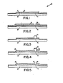
- Figures 1-5 illustrate the lift-off process for fabrication of sputtered dielectric gap material in a representative thin-film head 10.
- Figure 1 illustrates a substrate 12 a magnetic material 14, and a sputter deposit of approximately 8x10 -8 m of copper 16.
- Figure 2 illustrates a positive photoresist 18 which has been applied and an exposure to mask to open a back gap area 20, by way of example and for purposes of illustration through subsequent development.
- Figure 3 illustrates an electroplate through a photoresist-mask of copper 22 to a thickness in the range of approximately two to four times the desired gap thickness. This plated copper 22 assumes a mushroom shape and subsequently the photoresist 18 is removed as illustrated in the figure.
- Figure 4 illustrates sputter etching to remove exposed copper metallization and sputter deposition of a dielectric or nonmagnetic gap material 24 and 26 such as alumina, silicon nitride or quartz, as any other like dielectric or nonmagnetic gap material.
- figure 5 illustrates etching away the copper with a solution of twenty percent ammonium persulfate having a p H in the range of seven to nine.
- the lift-off process provides a magnetic closure region 28 with a contact surface 30 which is a clean geometrically defined hole with no dielectric material on the surface nor any attacking of the magnetic material 14.
- Figures 6-12 illustrate a specific embodiment of this invention for fabrication of read and write heads or read-write and servo heads with discrete gap dimensions on a single substrate.
- Figure 6 illustrates a side-by-side configuration, including a substrate 32, a magnetic material 34, and gap regions 36 and 37.
- Figure 7 illustrates plated copper 38 in the gap region 36, a back closure 40, and a back closure 42. The equal height is noted of the plated regions and closures.
- Figure 8 illustrates gap material such as alumina A1 2 0 3 , deposited to the desired thickness.
- Figure 9 illustrates photoresist covering 46 over the gap material and including no-resist covering at areas 48 and 50 while also protecting the plated copper at 40 and 42, as illustrated.
- Figure 10 illustrates etching away the exposed copper and lifting off the gap material and removing the resist. Note is made of the gap 36 and the specific back closures 40 and 42 as now illustrated with the gap material 44.
- Figure 11 illustrates depositing gap material 54 to a desired thickness, including over the previous gap material deposits 52.
- Figure 12 illustrates etching away the copper and lifting off the gap material, providing a gap region 36, a thickness of 54, and gap region 37 of thickness 44 and 54 with closure regions 58 and 60 devoid of any gap material.
- the lift-off process utilizes a copper coating that is removed by a solution of about twenty percent ammonium persulfate, (NH 4 ) 2 S 2 O 8 , having a pH of 7 to 9.
- An ammonium persulfate solution with a concentration in the range of 10 to 20 percent is used with 20 percent as a preferred optimum concentration.
- Ammonium persulfate becomes progressively less active as the concentration is decreased.
- the solution provides complete removal of gap. material from the back closure area of a thin film without damage to the underlying magnetic material.
- the addition of the sodium chloride tp the ammonium persulfate provides chloride ions in solution. 200 p.p.m. of sodium chloride provides 100 p.p.m. of chloride ions.
- the selection of sodium chloride provides a low cost source of chloride ions that does not change the pH of the solution.
- Other reagents with similar functions are calcium chloride and potassium chloride which also can be used.
- Ammonium chloride may also be used as both a source of chloride ions and as a means for the control or adjustment of the pH of the solution.
Landscapes
- Engineering & Computer Science (AREA)
- Chemical & Material Sciences (AREA)
- Manufacturing & Machinery (AREA)
- Power Engineering (AREA)
- Chemical Kinetics & Catalysis (AREA)
- General Chemical & Material Sciences (AREA)
- Materials Engineering (AREA)
- Mechanical Engineering (AREA)
- Metallurgy (AREA)
- Organic Chemistry (AREA)
- Magnetic Heads (AREA)
Applications Claiming Priority (2)
| Application Number | Priority Date | Filing Date | Title |
|---|---|---|---|
| US06/566,871 US4481071A (en) | 1983-12-29 | 1983-12-29 | Process of lift off of material |
| US566871 | 1995-12-04 |
Publications (2)
| Publication Number | Publication Date |
|---|---|
| EP0146796A2 true EP0146796A2 (de) | 1985-07-03 |
| EP0146796A3 EP0146796A3 (de) | 1988-06-01 |
Family
ID=24264747
Family Applications (1)
| Application Number | Title | Priority Date | Filing Date |
|---|---|---|---|
| EP84114282A Withdrawn EP0146796A3 (de) | 1983-12-29 | 1984-11-27 | Verfahren zur Herstellung von Dünnfilmmagnetkopfspalten durch Wegätzen |
Country Status (4)
| Country | Link |
|---|---|
| US (1) | US4481071A (de) |
| EP (1) | EP0146796A3 (de) |
| JP (1) | JPS60143416A (de) |
| CA (1) | CA1213044A (de) |
Families Citing this family (12)
| Publication number | Priority date | Publication date | Assignee | Title |
|---|---|---|---|---|
| US4652954A (en) * | 1985-10-24 | 1987-03-24 | International Business Machines | Method for making a thin film magnetic head |
| US4853080A (en) * | 1988-12-14 | 1989-08-01 | Hewlett-Packard | Lift-off process for patterning shields in thin magnetic recording heads |
| US5141623A (en) * | 1990-02-15 | 1992-08-25 | Seagate Technology, Inc. | Method for aligning pole tips in a thin film head |
| US5200056A (en) * | 1990-02-15 | 1993-04-06 | Seagate Technology Inc. | Method for aligning pole tips in a thin film head |
| US5087332A (en) * | 1991-08-05 | 1992-02-11 | Read-Rite Corp. | Process for making a thin film magnetic head with single step lift-off |
| US5256249A (en) * | 1991-09-17 | 1993-10-26 | Seagate Technology, Inc. | Method of manufacturing a planarized magnetoresistive sensor |
| DE4294247T1 (de) * | 1991-11-25 | 1994-01-13 | Digital Equipment Corp | Zwei-Schichten-Ätzprozess |
| US5572392A (en) * | 1994-11-17 | 1996-11-05 | International Business Machines Corporation | Arbitrary pattern write head assembly for writing timing-based servo patterns on magnetic storage media |
| US6090214A (en) * | 1998-06-22 | 2000-07-18 | Fujitsu Limited | Cleaning method using ammonium persulphate to remove slurry particles from CMP substrates |
| US20060108322A1 (en) * | 2004-11-19 | 2006-05-25 | Wei Wu | Lift-off material |
| US8432637B2 (en) | 2010-11-10 | 2013-04-30 | HGST Netherlands B.V. | Wet etching silicon oxide during the formation of a damascene pole and adjacent structure |
| CN105543846A (zh) * | 2016-02-05 | 2016-05-04 | 广东成德电子科技股份有限公司 | 印制电路板中性蚀刻剂及蚀刻方法 |
Family Cites Families (2)
| Publication number | Priority date | Publication date | Assignee | Title |
|---|---|---|---|---|
| US4119483A (en) * | 1974-07-30 | 1978-10-10 | U.S. Philips Corporation | Method of structuring thin layers |
| JPS5838851B2 (ja) * | 1978-09-28 | 1983-08-25 | シャープ株式会社 | 薄膜磁気ヘッドの作製方法 |
-
1983
- 1983-12-29 US US06/566,871 patent/US4481071A/en not_active Expired - Fee Related
-
1984
- 1984-09-26 CA CA000464112A patent/CA1213044A/en not_active Expired
- 1984-11-19 JP JP59242573A patent/JPS60143416A/ja active Granted
- 1984-11-27 EP EP84114282A patent/EP0146796A3/de not_active Withdrawn
Non-Patent Citations (2)
| Title |
|---|
| IBM TECHNICAL DISCLOSURE BULLETIN, vol. 22, no. 9, February 1980, page 4167, New York, US; S. DECKER et al.: "Masking process for magnetic head manufacture" * |
| IBM TECHNICAL DISCLOSURE BULLETIN, vol. 24, no. 4, September 1981, pages 1912-1913, New York, US; M. BARLOW et al.: "Thin film magnetic head assembly" * |
Also Published As
| Publication number | Publication date |
|---|---|
| CA1213044A (en) | 1986-10-21 |
| JPS60143416A (ja) | 1985-07-29 |
| EP0146796A3 (de) | 1988-06-01 |
| US4481071A (en) | 1984-11-06 |
| JPH0256721B2 (de) | 1990-12-03 |
Similar Documents
| Publication | Publication Date | Title |
|---|---|---|
| US4481071A (en) | Process of lift off of material | |
| JPH03252907A (ja) | 薄膜磁気ヘッドの製法 | |
| US4454014A (en) | Etched article | |
| EP0088869B1 (de) | Dünnfilmverfahren zur Herstellung von Ferritköpfen für schmale Spuren | |
| US4424271A (en) | Deposition process | |
| US4351698A (en) | Variable sloped etching of thin film heads | |
| US4224400A (en) | Method of manufacturing a magnetic head by photo-etching | |
| US6767477B2 (en) | Etching process to selectively remove copper plating seed layer | |
| JPH0681173A (ja) | 金属膜パターン形成方法 | |
| JPH037756B2 (de) | ||
| JPS5931770B2 (ja) | 磁気ヘツドのコアの製造方法 | |
| JPH036023A (ja) | 微細金属パターンの形成方法 | |
| JPS5855686B2 (ja) | 表面弾性波装置の製造方法 | |
| JPS6014453A (ja) | 金属層パタ−ンの形成方法 | |
| JP2993803B2 (ja) | センダスト・エッチング法 | |
| JPH06260478A (ja) | 薄膜パターン形成方法 | |
| JPH02123511A (ja) | 薄膜磁気ヘッド | |
| JPS6271231A (ja) | サセプタ | |
| JPS6214229B2 (de) | ||
| JPH05325136A (ja) | 薄膜磁気ヘッドの製造方法 | |
| JPH01173308A (ja) | 薄膜磁気ヘッドの製造方法 | |
| JPH05210823A (ja) | 薄膜磁気ヘッドの製造方法 | |
| JPS6233425A (ja) | 電極の形成方法 | |
| JPS60136906A (ja) | 薄膜磁気ヘツドの製造方法 | |
| JPH0371410A (ja) | 薄膜磁気ヘッドの製造方法 |
Legal Events
| Date | Code | Title | Description |
|---|---|---|---|
| PUAI | Public reference made under article 153(3) epc to a published international application that has entered the european phase |
Free format text: ORIGINAL CODE: 0009012 |
|
| 17P | Request for examination filed |
Effective date: 19841214 |
|
| AK | Designated contracting states |
Designated state(s): DE FR GB IT |
|
| PUAL | Search report despatched |
Free format text: ORIGINAL CODE: 0009013 |
|
| AK | Designated contracting states |
Kind code of ref document: A3 Designated state(s): DE FR GB IT |
|
| 17Q | First examination report despatched |
Effective date: 19900427 |
|
| 18W | Application withdrawn |
Withdrawal date: 19910308 |
|
| STAA | Information on the status of an ep patent application or granted ep patent |
Free format text: STATUS: THE APPLICATION HAS BEEN WITHDRAWN |
|
| R18W | Application withdrawn (corrected) |
Effective date: 19910308 |
|
| RIN1 | Information on inventor provided before grant (corrected) |
Inventor name: CHESNUTT, ROBERT BLAIR Inventor name: ANDERSON, NATHANIEL CARL Inventor name: DABY, LARRY EUGENE |