EP0148951A1 - System zum kontrollieren von abnormalitäten in programmierbarem kontroller - Google Patents
System zum kontrollieren von abnormalitäten in programmierbarem kontroller Download PDFInfo
- Publication number
- EP0148951A1 EP0148951A1 EP84901808A EP84901808A EP0148951A1 EP 0148951 A1 EP0148951 A1 EP 0148951A1 EP 84901808 A EP84901808 A EP 84901808A EP 84901808 A EP84901808 A EP 84901808A EP 0148951 A1 EP0148951 A1 EP 0148951A1
- Authority
- EP
- European Patent Office
- Prior art keywords
- address
- signal
- stored
- logic level
- sequence
- Prior art date
- Legal status (The legal status is an assumption and is not a legal conclusion. Google has not performed a legal analysis and makes no representation as to the accuracy of the status listed.)
- Granted
Links
Images


Classifications
-
- G—PHYSICS
- G05—CONTROLLING; REGULATING
- G05B—CONTROL OR REGULATING SYSTEMS IN GENERAL; FUNCTIONAL ELEMENTS OF SUCH SYSTEMS; MONITORING OR TESTING ARRANGEMENTS FOR SUCH SYSTEMS OR ELEMENTS
- G05B19/00—Program-control systems
- G05B19/02—Program-control systems electric
- G05B19/04—Program control other than numerical control, i.e. in sequence controllers or logic controllers
- G05B19/05—Programmable logic controllers, e.g. simulating logic interconnections of signals according to ladder diagrams or function charts
- G05B19/058—Safety, monitoring
-
- G—PHYSICS
- G05—CONTROLLING; REGULATING
- G05B—CONTROL OR REGULATING SYSTEMS IN GENERAL; FUNCTIONAL ELEMENTS OF SUCH SYSTEMS; MONITORING OR TESTING ARRANGEMENTS FOR SUCH SYSTEMS OR ELEMENTS
- G05B2219/00—Program-control systems
- G05B2219/10—Plc systems
- G05B2219/13—Plc programming
- G05B2219/13037—Tracing
-
- G—PHYSICS
- G05—CONTROLLING; REGULATING
- G05B—CONTROL OR REGULATING SYSTEMS IN GENERAL; FUNCTIONAL ELEMENTS OF SUCH SYSTEMS; MONITORING OR TESTING ARRANGEMENTS FOR SUCH SYSTEMS OR ELEMENTS
- G05B2219/00—Program-control systems
- G05B2219/10—Plc systems
- G05B2219/14—Plc safety
- G05B2219/14098—Displaying instructions for monitoring state of machine
Definitions
- the present invention relates to a sequence abnormality check system in a programmable controller so as to check a cause of failure when abnormality occurs in processing results of the programmable controller.
- a sequence circuit is arranged between a control device and a machine to be controlled.
- the sequence circuit comprises a heavy current circuit consisting of a number of relays.
- a predetermined relay is operated in response to an. instruction from the control device so as to cause machine members to perform a predetermined operation in accordance with this instruction.
- information for the sequence circuit is stored in the form of a program in a memory of the PC, thereby performing sequence control.
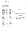
- sequence circuit is exemplified by a ladder diagram represented by relay symbols, as shown in Fig. 1.
- a sequence program having a logical sequence of instruction codes and operands shown in Fig. 2 is stored in a memory of the PC, thereby achieving proper sequence control.
- the ladder diagram shown in Fig. 1 comprises part of a ladder diagram of a numerical control (NC). machine tool system. Symbols ⁇ and denote normally open and closed contacts of relays (not shown) each having a reference symbol.
- M03 spindle forward rotation instruction
- relays MF, M12 and M11 are operated to energize a relay M03X.
- a relay AUT is kept ON.
- a relay SPCCW is kept OFF
- a relay SPCW is turned on. This indicates that the spindle forward rotation instruction is supplied to a machine such as a machine tool.
- the high current circuit having the relays represented by the ladder diagram controls the sequence of the machine tool.
- the PC creates a sequence program of Fig. 2 in accordance with the ladder diagram, and the sequence program is stored in a memory so as to provide sequence control.
- "RD”, "AND”, “WRT”, “OR”, “AND-NOT”, etc. in the sequence program are instruction codes, respectively. More specifically, RD is a read instruction; AND, a logical product operation instruction; WRT, a write instruction; OR, a logical sum operation instruction; and AND-NOT, an inversion/logical product instruction.
- Numeric values in the operand column represent addresses of a data memory (to be described later) incorporated in the PC.
- the addresses correspond to relay symbols (MF, M28, etc.) of Fig. 1, respectively. The relationship between the relay symbol and the address is illustrated in Fig. 1.
- the relay symbols are listed for reference at the right of the table in Fig. 2.
- the information at the addresses of the data memory which are described in the column of operands is calculated by an instruction group Dl of the sequence program.
- a logical operation MF ⁇ M28 ⁇ M24 ⁇ M22 ⁇ M21 ⁇ M18 ⁇ M14 ⁇ M12 ⁇ M11 is calculated.
- a calculation result (“1" or "0") is stored at address 10.2 of the data memory which corresponds to the relay M03 X .
- the following operation is performed in accordance with an instruction group D2:
- a calculation result is stored at address 20.5 of the data memory which is designated by the operand SPCW.
- a spindle forward rotation signal is supplied to the machine tool as an external machine, so that the spindle of the machine tool is rotated in the forward direction.
- the sequence control system having the PC is operated in accordance with the sequence program. In this control system, when an intermittent and instantaneous failure of the sequence occurs during automatic operation of the machine tool, it is difficult to determine the cause.
- a feed hold circuit is illustrated in Fig. 3A.
- Reference symbol a denotes a feed hold button; b, a pressure decrease detection switch; and SP, a feed hold relay.
- This feed hold circuit is represented by a ladder diagram in Fig. 3B. Since the machine tool is interrupted in the feed hold state, the feed hold relay SP is stopped. When a signal (i.e., logic level of the signal at address 102.5 of the data memory which represents the feed hold relay SP) representing the operating state of the feed hold relay SP is checked, "1" is stored at address 102.5. The logic level "1" indicates that the feed hold relay SP is normally operated. This indicates that the contact of the feed hold button or the pressure decrease detection switch might have been accidentally and temporarily opened during automatic operation.
- PC programmable controller
- a sequence abnormality check system having: an address setting means for setting a read address for reading out signals representing states of elements of a sequence circuit for performing sequence control in the PC; and a storage means consisting of an address setting table for storing an address set by the address setting means and a logic level of a signal of the address and a signal update storage table for storing an address signal updating order and their logic levels, wherein the logic level of the signal stored at an address of the address setting table is compared with a logic level of the actual signal; if they are different from each other, in response to the signal from a signal update detecting means, a signal update writing means writes in the signal update storage table the address at which the signal is updated, the logic level of the actual signal at the address, and a mark representing last updating, and at the same time, updates the logic level of the signal at the address of the address setting table to the logic level of the actual signal; when addresses associated with the failure upon occurrence of the failure are read out from the address setting means and
- sequence abnormality check system in the program controller of the present invention, when any element of the sequence circuit which is not supposed to be operated is instantaneously operated to cause a failure such as stop of the machine tool, the logic levels of the updated signals at addresses corresponding to the elements subjected to the failure, and an updating order are displayed upon setting these addresses. As a result, the cause of the failure can be immediately determined, thereby quickly restoring the system.
- Fi g . 4 is a block diagram of a PC which employs the present invention.
- Reference numeral 1 denotes a sequence control means.
- the sequence control means 1 receives an input signal from a machine such as an NC machine tool through an input circuit 4 and a signal which is supplied from a control relay 6 in the sequence circuit and which is stored in the PC.
- the sequence control means 1 then generates an output signal to the machine through an output circuit 5 in accordance with the sequence program, thereby controlling the sequence of the machine.
- the PC of the present invention has a signal update detecting means 2, a signal update writing means 3, an address setting means 7, and a storage means.
- the storage means has an address setting table TA and a signal update storage table TB.
- the address setting means 7 sets addresses of the data memory of the PC which store logic levels of the respective elements of the sequence circuit.
- an address associated therewith is set by the address setting means 7 in the address setting table TA.
- the address setting table TA also stores the entered address and a logic level of a signal at this address.
- the signal update detecting means 2 compares the logic level of the signal at the address of the address setting table TA with a corresponding actual signal. In other words, the signal update detecting means 2 compares the logic levels of the signals at addresses of the data memory which respectively correspond to the input circuit 4, the output circuit 5 and the control relay 6. When the signal update detecting means 2 detects updating of the signal, the signal update writing means 6 updates the logic level at the address of the address setting table TA to that of the actual signal.
- this address, the logic level of the signal at this address, and a signal representing the last updated signal are stored in the signal update storage table TB.
- the signal update storage table TB stores an updated signal address order and the corresponding logic levels of the addresses.
- An address associated with the failure is entered at the address setting means 7 in accordance with the ladder diagram and is stored in the address setting table TA.
- the signal update detecting means 2 compares the logic level of the actual signal at the address of the address setting table TA with the logic level (upon initialization, the logic level is set at "0" or "1") corresponding to this address.
- the updated logic level is stored at the corresponding address of the signal update storage table TB.
- the logic level of the actual signal is stored in the address setting table TA.
- the signal update storage table TB stores an address order representing updating of the logic levels and the updated logic levels at the addresses.
- a signal representing the last updated signal is assigned at the last updated address.
- Fig. 5 is a block diagram of PC hardware according to the present invention.
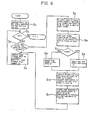
- Fig. 6 is a flow chart for explaining the operation of the PC hardware.
- reference numeral 11 denotes a ROM for storing a control program for controlling the overall operation of the PC.
- Reference numeral 12 denotes a ROM for storing a sequence program and a signal update detection program.
- Reference numeral 13 denotes a data memory comprising a RAM for storing logic levels of signals representing the respective elements of the sequence circuit which are represented by relay symbols in Figs. 1 and 3B.
- Reference numeral 10 denotes a microprocessor (MPU) for performing predetermined sequence processing in accordance with the control program and the sequence program.
- MPU microprocessor
- the MPU 10, the ROM 11 for storing the control program, the ROM 12 for storing the sequence program and the signal update detection program, and the data memory 13 for storing logic levels of signals which represent the operating states of the respective elements of the sequence circuit constitute the sequence control means 1, the signal update detecting means 2 and the signal update writing means of Fig. 4.
- Reference numeral 14 denotes a storage hold memory for storing the address setting table TA and the signal update storage table TB; and 16, a display unit for displaying the tables TA and TB stored in the storage hold memory 14.
- the display unit 16 comprises a CRT or a printer.
- Reference numeral 15 denotes a keyboard input means used as the address setting means 7 of Fig. 4 when the address associated with the failure upon occurrence thereof is entered for the data memory.
- Reference numerals 4 and 5 denote input and output circuits for connecting the NC machine or a machine tool to the PC, respectively.
- Reference numeral 17 denotes a bus.
- the PC having the arrangement described above controls the sequence of the external machine in accordance with the sequence program stored in the ROM 12.
- the signals each having a predetermined logic level are stored at predetermined addresses of the data memory 13 by input and output signals from the input and output cicuits 4 and 5.
- the logic levels of these signals represent the operating states of the elements of the sequence circuit.
- the operator determines an address of a sequence element associated with the failure in accordance with the ladder diagram. This value is entered at the keyboard 15 as the address setting means 7 and is stored in the address setting table TA in the storage hold memory 14, as shown in Fig. 7.
- the logic level of the address signal may be entered at the address setting means 6. Otherwise, any logic level "1" or "0" is stored in the address setting table TA.
- the MPU 10 in the PC checks from the beginning of the address setting table TA whether or not the address is set in the address setting table TA (Sl of Fig. 6) after one sequence control cycle is completed.
- the MPU 10 checks whether or not the signal set in the address setting table TA has the same logic level as that of the actual signal (i.e., the MPU 10 compares the logic levels of the signals which represent the operating states of the input and output circuits 4 and 5 and the control relay 6 and which are stored in the data memory 13) (S2 and S3 of Fig. 6). If YES, the address with the next line number of the address setting table TA is subjected to comparison in the same manner-as described above (S4 of Fig. 6). When there is any signal having the logic level in the address setting table TA different from that of the actual signal, the logic level of this signal in the address setting table TA is updated to that of the corresponding actual signal (S5 of Fig.
- the MPU 10 searches for a line number which stores the last updated signal in the signal update storage table TB in the storage hold memory 14; if not, no last updated signal is stored in the signal update storage table TB. Table number 1 is selected. When the last updated signal is present there, the next line number is selected (S6, S7, S8 and S9 of Fig. 61. The corresponding address and the corresponding logic level are stored in the selected line number memory location in the address setting table TA (S10 of Fig. 6). A signal (e.g., a mark) representing the last updated signal is stored at this memory location. The previously assigned mark in the table is deleted (Sll of Fig. 6). A line number next to the currently selected line number of the address setting table TA is selected (S4 of Fig. 61, and the same operation (S2, S3, S4, S5,... of Fig. 6) as described above will be performed.
- the MPU 10 repeatedly performs the above processing every time one sequence control cycle is completed.
- the address setting table TA stores the logic levels of current signals at the set addresses.
- the signal update storage table TB stores an address order representing updating of the signals at the addresses of the address setting table TA, and the logic levels of the current signals. Since the memory capacity of the signal update storage table TB is limited and the signal update storage table TB is used in a circulatory manner, the mark is assigned at the address for storing the last updated signal in the signal update storage table TB. The mark represents the updated address order.
- the addresses at which the logic levels of the signals are updated, and an order of updating can be visually checked. Therefore, the operator can easily check the address supposed not to be updated (i.e., the element supposed not to be operated), thereby simplifying failure check.
- the relay represented at address 31.5 is turned off, so that the actual signal is set at logic level "1"; the logic level of the signal stored at address 31.5 in the address setting table TA is different from that of the actual signal (S2 and S3 of Fig. 6), so that the logic level of the signal stored at address 31.5 is updated to logic level "1"; and, as shown in Fig. 8, the signal update storage table TB stores address 31.5 and logic level "1" (S5, S6, S7, S8, S10 and Sll of Fig. 6).
- the relay represented by address 31.5 is turned on, the normally closed contact a' is opened, and the feed hold relay SP is turned off.
- the logic level of the signal stored at the actual address 102.5 becomes “0” and is different from the logic level "1" of the signal stored in the address setting table TA; the logic level of the signal in the address setting table TA is updated to "0" (S3 and S5 of Fig. 6); and, as shown in Fig. 9, address 102.5 and the corresponding logic level "0" are stored in the signal update storage table T B (S6, S7, S9, S10 and (S11) of Fig. 6).
- the relay represented by address 31.5 When the feed hold button a is turned on, the relay represented by address 31.5 is turned off, and the corresponding logic level becomes "0".
- the logic level of the signal in the table TB is different from that in the address setting table TA.
- the logic level of the signal stored at address 31.5 of the address setting table TA is set to "0".
- the same address and logic level as described above are stored with line number 3 in the signal update storage table TB in Fig. 8. Since the normally closed contact of the relay represented by address 31.5 becomes ON, the feed hold relay SP is turned on.
- the logic level of the actual signal at address 102.5 becomes "1" and is different from that in the address setting table TA.
- the logic level of the signal stored at address 102.5 of the address setting table TA is updated to logic "1".
- This address 102.5 is stored as an updated address with line number 4 of the signal update storage table TB.
- the corresponding logic level "1" is also stored in the table TB.
- the last updated mark is changed from line number 3 to line number 4 of the signal update storage table TB (It should be noted that the mark has not been described in the preceding part of the specification, but that the mark has been actually relabeled from line number 1 to line number 2, line number 2 to line number 3 and line number 3 to line number 4 of the signal update storage table TB).
- the logic levels of the signals from the input and output circuits are stored in the data memory.
- the signals from the input and output signals need not be stored in the data memory. Addresses are assigned to the respective terminals of the input and output circuits.
- the logic levels of the signals may be read out from the data memory for storing the signals having logic levels representing the operating states of the terminals of the input and output circuits and the control relay in response to the address entered at the address setting means.
Landscapes
- Physics & Mathematics (AREA)
- General Physics & Mathematics (AREA)
- Engineering & Computer Science (AREA)
- Automation & Control Theory (AREA)
- Programmable Controllers (AREA)
- Testing And Monitoring For Control Systems (AREA)
Applications Claiming Priority (2)
| Application Number | Priority Date | Filing Date | Title |
|---|---|---|---|
| JP58079354A JPS59205614A (ja) | 1983-05-09 | 1983-05-09 | プログラマブルコントロ−ラにおけるシ−ケンス異常チエツク方式 |
| JP79354/83 | 1983-05-09 |
Publications (3)
| Publication Number | Publication Date |
|---|---|
| EP0148951A1 true EP0148951A1 (de) | 1985-07-24 |
| EP0148951A4 EP0148951A4 (de) | 1987-07-27 |
| EP0148951B1 EP0148951B1 (de) | 1992-01-15 |
Family
ID=13687562
Family Applications (1)
| Application Number | Title | Priority Date | Filing Date |
|---|---|---|---|
| EP84901808A Expired EP0148951B1 (de) | 1983-05-09 | 1984-05-04 | System zum kontrollieren von abnormalitäten in programmierbarem kontroller |
Country Status (5)
| Country | Link |
|---|---|
| US (1) | US4633384A (de) |
| EP (1) | EP0148951B1 (de) |
| JP (1) | JPS59205614A (de) |
| DE (1) | DE3485459D1 (de) |
| WO (1) | WO1984004610A1 (de) |
Cited By (3)
| Publication number | Priority date | Publication date | Assignee | Title |
|---|---|---|---|---|
| EP0263188A4 (de) * | 1986-04-15 | 1989-12-13 | Fanuc Ltd | Signalprüfungssteuerungssystem für eine regeleinrichtung einer programmierbaren maschine. |
| GB2253720A (en) * | 1991-03-14 | 1992-09-16 | Toyota Motor Co Ltd | Diagnostic system for programmable controller |
| WO1993018441A1 (en) * | 1992-03-09 | 1993-09-16 | Electronic Data Systems Corporation | Method and system for automatic graphic display modification based on control program modification |
Families Citing this family (9)
| Publication number | Priority date | Publication date | Assignee | Title |
|---|---|---|---|---|
| JPH0670764B2 (ja) * | 1985-03-06 | 1994-09-07 | 株式会社日立製作所 | シ−ケンス制御装置 |
| US4851985A (en) * | 1985-04-15 | 1989-07-25 | Logitek, Inc. | Fault diagnosis system for comparing counts of commanded operating state changes to counts of actual resultant changes |
| US5133066A (en) * | 1985-10-24 | 1992-07-21 | International Business Machines Corporation | Method for selecting multiple versions of data in a reduced record units text editing system |
| GB2200476B (en) * | 1987-01-29 | 1991-02-06 | British Gas Plc | Monitor system |
| JPH0677216B2 (ja) * | 1987-05-25 | 1994-09-28 | マツダ株式会社 | シ−ケンスプログラム制御系のモニタ装置 |
| JP2792772B2 (ja) * | 1991-04-01 | 1998-09-03 | 三菱電機株式会社 | プログラマブルコントローラ及びそのシーケンスプログラムモニタ方法 |
| US5870693A (en) * | 1996-03-01 | 1999-02-09 | Sony Display Device (Singapore) Pte. Ltd. | Apparatus and method for diagnosis of abnormality in processing equipment |
| US7419467B2 (en) * | 1998-11-25 | 2008-09-02 | M3 Electronics, Inc. | Medical inspection device |
| RU2239218C1 (ru) * | 2003-05-05 | 2004-10-27 | Северо-Кавказский государственный технический университет | Устройство для контроля радиоэлектронных объектов |
Family Cites Families (8)
| Publication number | Priority date | Publication date | Assignee | Title |
|---|---|---|---|---|
| JPS5332030B2 (de) * | 1972-01-18 | 1978-09-06 | ||
| JPS5518362B2 (de) * | 1974-10-21 | 1980-05-19 | ||
| US3997879A (en) * | 1975-12-24 | 1976-12-14 | Allen-Bradley Company | Fault processor for programmable controller with remote I/O interface racks |
| US4062061A (en) * | 1976-04-15 | 1977-12-06 | Xerox Corporation | Error log for electrostatographic machines |
| JPS52149580A (en) * | 1976-06-08 | 1977-12-12 | Kyosan Electric Mfg Co Ltd | Record memorizing method |
| US4063311A (en) * | 1976-08-17 | 1977-12-13 | Cincinnati Milacron Inc. | Asynchronously operating signal diagnostic system for a programmable machine function controller |
| JPS57206923A (en) * | 1981-06-15 | 1982-12-18 | Hitachi Ltd | External trouble diagnosing device for process controller |
| DE3206891A1 (de) * | 1982-02-26 | 1983-09-15 | Robert Bosch Gmbh, 7000 Stuttgart | Verfahren zur fehlerdiagnose fuer speicherprogrammierbare steuerungen |
-
1983
- 1983-05-09 JP JP58079354A patent/JPS59205614A/ja active Pending
-
1984
- 1984-05-04 US US06/695,362 patent/US4633384A/en not_active Expired - Fee Related
- 1984-05-04 EP EP84901808A patent/EP0148951B1/de not_active Expired
- 1984-05-04 DE DE8484901808T patent/DE3485459D1/de not_active Expired - Lifetime
- 1984-05-04 WO PCT/JP1984/000227 patent/WO1984004610A1/ja not_active Ceased
Cited By (4)
| Publication number | Priority date | Publication date | Assignee | Title |
|---|---|---|---|---|
| EP0263188A4 (de) * | 1986-04-15 | 1989-12-13 | Fanuc Ltd | Signalprüfungssteuerungssystem für eine regeleinrichtung einer programmierbaren maschine. |
| GB2253720A (en) * | 1991-03-14 | 1992-09-16 | Toyota Motor Co Ltd | Diagnostic system for programmable controller |
| GB2253720B (en) * | 1991-03-14 | 1994-08-03 | Toyota Motor Co Ltd | Diagnostic system for programmable controller |
| WO1993018441A1 (en) * | 1992-03-09 | 1993-09-16 | Electronic Data Systems Corporation | Method and system for automatic graphic display modification based on control program modification |
Also Published As
| Publication number | Publication date |
|---|---|
| US4633384A (en) | 1986-12-30 |
| EP0148951A4 (de) | 1987-07-27 |
| EP0148951B1 (de) | 1992-01-15 |
| WO1984004610A1 (fr) | 1984-11-22 |
| DE3485459D1 (de) | 1992-02-27 |
| JPS59205614A (ja) | 1984-11-21 |
Similar Documents
| Publication | Publication Date | Title |
|---|---|---|
| EP0148951A1 (de) | System zum kontrollieren von abnormalitäten in programmierbarem kontroller | |
| US4616307A (en) | Programmable controller alarm display method | |
| EP0436035B1 (de) | Verfahren zur Anzeige der Betriebsgeschichte einer Maschine | |
| JPS60262204A (ja) | プログラマブル・コントロ−ラ | |
| EP0164421B1 (de) | Programmierbares kontrollgerät | |
| EP0121570A1 (de) | Aufzeichnungsverfahren eines diagnoseresultats | |
| US4887220A (en) | Parameter initializing method for a programmable machine controller | |
| JP3359562B2 (ja) | プログラム式表示装置用の表示画面作成方法 | |
| JPH0577143A (ja) | 自動化ラインの故障診断装置 | |
| JPH0152762B2 (de) | ||
| EP0408761A1 (de) | Verfahren zum sicheren betrieb eines roboters | |
| JPS6184712A (ja) | プログラマブルコントロ−ラ | |
| JPS63194921A (ja) | アラ−ムの種類に応じてアラ−ム表示の色を変える射出成形機 | |
| EP0525941A2 (de) | Verfahren zur Selbstdiagnose eines mobilen Fernsprechapparats zum Gebrauch in einem mobilen Fernsprechvermittlungssystem und auf dieses Verfahren angewandeter Fernsprechapparat | |
| JPS6155702A (ja) | 数値制御装置 | |
| JPS5916014A (ja) | シ−ケンスコントロ−ラにおける異常チエツク方式 | |
| JPH0411881B2 (de) | ||
| JPS5929882B2 (ja) | シ−ケンスコントロ−ラ | |
| JPS627563B2 (de) | ||
| JPH02176805A (ja) | 入出力制御に関する故障診断装置 | |
| JPS6250841B2 (de) | ||
| JPH07271411A (ja) | プログラマブル・コントローラの故障診断装置 | |
| JPS585858A (ja) | システム再開処理方式 | |
| JPH08123513A (ja) | プログラマブルコントローラのデータモニタ装置 | |
| JPH0321922B2 (de) |
Legal Events
| Date | Code | Title | Description |
|---|---|---|---|
| PUAI | Public reference made under article 153(3) epc to a published international application that has entered the european phase |
Free format text: ORIGINAL CODE: 0009012 |
|
| 17P | Request for examination filed |
Effective date: 19850123 |
|
| AK | Designated contracting states |
Designated state(s): DE FR GB |
|
| A4 | Supplementary search report drawn up and despatched |
Effective date: 19870727 |
|
| 17Q | First examination report despatched |
Effective date: 19890131 |
|
| RBV | Designated contracting states (corrected) |
Designated state(s): DE |
|
| GRAA | (expected) grant |
Free format text: ORIGINAL CODE: 0009210 |
|
| AK | Designated contracting states |
Kind code of ref document: B1 Designated state(s): DE |
|
| REF | Corresponds to: |
Ref document number: 3485459 Country of ref document: DE Date of ref document: 19920227 |
|
| PLBE | No opposition filed within time limit |
Free format text: ORIGINAL CODE: 0009261 |
|
| STAA | Information on the status of an ep patent application or granted ep patent |
Free format text: STATUS: NO OPPOSITION FILED WITHIN TIME LIMIT |
|
| 26N | No opposition filed | ||
| PG25 | Lapsed in a contracting state [announced via postgrant information from national office to epo] |
Ref country code: DE Effective date: 19930202 |