EP0150421A1 - Système à tableau sensible au toucher et aux variations de capacité - Google Patents
Système à tableau sensible au toucher et aux variations de capacité Download PDFInfo
- Publication number
- EP0150421A1 EP0150421A1 EP84115648A EP84115648A EP0150421A1 EP 0150421 A1 EP0150421 A1 EP 0150421A1 EP 84115648 A EP84115648 A EP 84115648A EP 84115648 A EP84115648 A EP 84115648A EP 0150421 A1 EP0150421 A1 EP 0150421A1
- Authority
- EP
- European Patent Office
- Prior art keywords
- lines
- antenna
- sense
- touch
- drive
- Prior art date
- Legal status (The legal status is an assumption and is not a legal conclusion. Google has not performed a legal analysis and makes no representation as to the accuracy of the status listed.)
- Granted
Links
Images






Classifications
-
- H—ELECTRICITY
- H03—ELECTRONIC CIRCUITRY
- H03K—PULSE TECHNIQUE
- H03K17/00—Electronic switching or gating, i.e. not by contact-making and –breaking
- H03K17/94—Electronic switching or gating, i.e. not by contact-making and –breaking characterised by the way in which the control signals are generated
- H03K17/96—Touch switches
- H03K17/9618—Touch switches using a plurality of detectors, e.g. keyboard
-
- G—PHYSICS
- G06—COMPUTING OR CALCULATING; COUNTING
- G06F—ELECTRIC DIGITAL DATA PROCESSING
- G06F3/00—Input arrangements for transferring data to be processed into a form capable of being handled by the computer; Output arrangements for transferring data from processing unit to output unit, e.g. interface arrangements
- G06F3/01—Input arrangements or combined input and output arrangements for interaction between user and computer
- G06F3/03—Arrangements for converting the position or the displacement of a member into a coded form
- G06F3/041—Digitisers, e.g. for touch screens or touch pads, characterised by the transducing means
- G06F3/044—Digitisers, e.g. for touch screens or touch pads, characterised by the transducing means by capacitive means
- G06F3/0446—Digitisers, e.g. for touch screens or touch pads, characterised by the transducing means by capacitive means using a grid-like structure of electrodes in at least two directions, e.g. using row and column electrodes
-
- H—ELECTRICITY
- H03—ELECTRONIC CIRCUITRY
- H03K—PULSE TECHNIQUE
- H03K17/00—Electronic switching or gating, i.e. not by contact-making and –breaking
- H03K17/94—Electronic switching or gating, i.e. not by contact-making and –breaking characterised by the way in which the control signals are generated
- H03K17/96—Touch switches
- H03K17/962—Capacitive touch switches
- H03K17/9622—Capacitive touch switches using a plurality of detectors, e.g. keyboard
-
- H—ELECTRICITY
- H03—ELECTRONIC CIRCUITRY
- H03K—PULSE TECHNIQUE
- H03K17/00—Electronic switching or gating, i.e. not by contact-making and –breaking
- H03K17/94—Electronic switching or gating, i.e. not by contact-making and –breaking characterised by the way in which the control signals are generated
- H03K17/96—Touch switches
- H03K2017/9602—Touch switches characterised by the type or shape of the sensing electrodes
- H03K2017/9604—Touch switches characterised by the type or shape of the sensing electrodes characterised by the number of electrodes
-
- H—ELECTRICITY
- H03—ELECTRONIC CIRCUITRY
- H03K—PULSE TECHNIQUE
- H03K17/00—Electronic switching or gating, i.e. not by contact-making and –breaking
- H03K17/94—Electronic switching or gating, i.e. not by contact-making and –breaking characterised by the way in which the control signals are generated
- H03K17/96—Touch switches
- H03K2017/9602—Touch switches characterised by the type or shape of the sensing electrodes
- H03K2017/9604—Touch switches characterised by the type or shape of the sensing electrodes characterised by the number of electrodes
- H03K2017/9613—Touch switches characterised by the type or shape of the sensing electrodes characterised by the number of electrodes using two electrodes per touch switch
Definitions
- the present invention pertains to improvements in capacitance-variation-sensitive touch sensing array systems.
- a touch sensing array system includes an array of touch elements which may be operated as keys on a keyboard or to provide an indication associated with a given position in the array.
- touch elements In a capacitance-variation-sensitive touch sensing array system the touching of a touch element results in a variation of the capacitance between the touch element and circuit ground. This variation results in the variation of a sense signal produced on one or more sense lines coupled to the respective touch element.
- the sense signals are processed to provide information associated with any particular touch element that is touched by an operator.
- each touch element is driven by an alternating current signal. Sense signals are produced on the respective sense lines coupled to the respective touch elements when the touch element is driven.
- the present invention provides an improved capacitance-variation-sensitive touch sensing array system for which the array may be inexpensively fabricated in a monolithic construction that is easy to maintain.
- the nature of the basic combination of elements in the system provides the following advantages:
- the capacitance-variation-sensitive touch sensing array system of the present invention includes an array of antenna lines; an array of touch elements, with each touch element being coupled to one or more antenna lines of the antenna line array to vary the capacitance between each of the coupled antenna lines and ground upon the touch element coupled thereto being touched by an operator; an array of drive lines coupled to the antenna lines; a drive signal generator for applying drive signals to the drive lines to drive the antenna lines coupled thereto; an array of sense lines coupled to the antenna lines to derive sense signals from the antenna lin6s when drive signals are applied to the drive lines; and means coupled to the sense lines for sensing the sense signals on the respective sense lines, with the amplitudes of the respective sense signals being dependent upon whether the capacitance between the respective driven antenna line and circuit ground is varied by an operator touching the touch element coupled to the driven antenna line; and a signal processing system coupled to the sensing means for processing the sense signals to provide information associated with any particular touch element that is touched by an operator.
- each antenna line is coupled to only one drive line and to only one sense line; each of the drive lines is coupled to a plurality of antenna lines; each of the sense lines is coupled to a plurality of antenna lines; no given drive line and sense line pair is connected to more than one antenna line in common; and the drive signal generator is adapted for repetitively applying a sequence of drive signals having different predetermined characteristics to the different drive lines to cause differently characterized sense signals to be derived on a sense line coupled to a plurality of different antenna lines. It is also preferable that the drive signals are alternating signal packets that differ from each other by being nonsynchronous and/or by being of opposing polarities if synchronous with each other.
- the different drive signals in combination include nonsynchronous sets of pulsed signal packet pairs, with the paired signal packets in each set being synchronous with each other, of approximately the same value, and of opposing polarities to thereby cause the amplitude of the sense signals derived in response to said synchronous pairs of drive signal packets to be low in relation to the variation in the amplitude of the sense signals resulting from the touch elements being touched by an operator.
- This feature enables the number of sense signals and related sense signal processing to be reduced by fifty percent.
- the touch sensing array is amenable to an inexpensive monolithic construction, wherein a first portion of the antenna array is supported by one side of a thin dielectric substrate and a second portion of the antenna array is supported by the opposite side of the thin dielectric substrate.
- the touch elements individually include a first tab supported by the one side of the substrate and extending from an antenna line of the first portion of the array; and a second tab supported by the opposite side of the substrate and extending from an antenna line of the second portion of the array adjacent to the position underlying the first tab so that the capacitance between both antenna lines and ground is varied when the touch element is touched by an operator in the proximity of both tabs.
- the drive lines and sense lines are supported by opposite sides of a second thin dielectric substrate that is separated by a third thin dielectric substrate from the first-mentioned dielectric substrate supporting the antenna arrays; or the drive lines and sense lines are supported on the same thin dielectric substrate as the antenna arrays.
- a drive line or sense line on one side of the substrate is coupled to an antenna line on the opposite side of the substrate by a capacitor including a first plate supported by the one side of the substrate and extending from the coupled drive line or sense line; and a second plate supported by the opposite side of the substrate and extending from the coupled antenna line and underlying the first plate.
- the touch sensing array system of the present invention can be configured for use as a keyboard.
- the antenna lines are arrayed in rows and columns and each touch element is coupled to one row antenna line and to one column antenna line.
- the touch elements function as keys of the keyboard.
- the sense signals derived from the row and column antenna lines are processed to provide signals associated with whichever key is touched by an operator.
- the touch sensing array system of the present invention also can be configured so that finger touch position can be sensed.
- individual touch elements are coupled to only one antenna line of the array and are dimensioned and disposed so that an operator firmly touching an interior touch element of the array with his finger necessarily touches a plurality of touch elements simultaneously; and the signal processing system processes the sense signals to provide information associated with the position in the array of any particular touch element that is touched by an operator.
- the processing system processes the relative magnitudes of the sense signal value variations resulting from a plurality of the touch elements being touched, and performs an interpolation routine using such relative magnitudes to provide an estimate of touch position.
- sense signal values are provided in accordance with the amplitudes of the respective sense signals and the processing system processes the sense signals iteratively to ascertain the values of variations in the sense signal values and for processing the variation values to determine whether any said variation resulted from a touch element being touched by an operator.
- the processing of variation values allows more powerful and versatile processing routines to be used to more accurately recognize a valid touch by an operator.
- sense signal values are provided in accordance with the amplitudes of the respective sense signals and the processing system processes the sense signals iteratively to determine whether any of the touch elements has been touched by an operator by comparing the sense signal values with baseline values derived from sense signal values provided when the touch elements are untouched by an operator to determine whether a variation value derived from said comparison exceeds a predetermined threshold value; and revises the baseline values in response to sensed variations in the sense signal values over a predetermined number of iterations occurring in the absence of valid touch by an operator.
- This feature allows portions of the touch element array not in use to be covered with nonconducting materials, such as books or papers, without rendering the array inoperative.
- a preferred embodiment of the capacitance-variation-sensitive touch sensing array system of the present invention includes a 32 x 32 touch element array 10, an antenna line array that includes thirty-two row antenna lines Al-32 and thirty-two column antenna lines A33-64, a drive line array that includes four row drive lines DLI-4 and four column drive lines D L5-8, an array of eight sense lines SL1-8, an array of sixty-four drive line-to-antenna capacitors DLACl-64, an array of sixty-four antenna-to-sense line capacitors ASLCI-64, a multiplexer 11, an amplifier circuit 12, a synchronous demodulator 13, an analog-to-digital (A/D) converter 14, a microprocessor 15, a control logic circuit 16 and a drive signal generator 17.
- A/D analog-to-digital
- each of the touch elements TE is connected to one of the row antenna lines Al-32 and to one of the column antenna lines A33-64.
- Each of the antenna lines Al-64 is connected to thirty-two touch elements TE.
- the drive lines Dl-8 are capacitively coupled to the antenna lines A l-64 by the drive line-to-antenna capacitors DLACl-64.
- the antenna lines Al-64 are capacitively coupled to the sense lines SL1-8 by the antenna-to-sense line capacitors ASLCl-64.
- Each antenna line Al-64 is capacitively coupled to only one drive line DL and to only one sense line SL.
- Each of the eight drive lines DL1-8 is capacitively coupled to eight of the sixty-four antenna lines Al-64; and each of the eight sense lines SL1-8 is coupled to eight of the sixty-four antenna lines Al-64.
- each antenna line Al-64 completes a T-bridge connection between a pair made up of a unique one of drive lines D Ll-8 and a unique one of sense lines SL1-8.
- each touch element TE is shown as connected to an antenna line A.
- a drive line DL is capacitively coupled to the antenna line A by the drive-line-to-antenna capacitance D L AC; and the antenna line A is capacitively coupled to a sense line SL by an antenna-to-sense line capacitance ASLC.
- a drive signal is provided on the drive line DL by a drive signal source V to drive the antenna line A.
- the touch element TE provides a variable capacitance to ground (VCG) in accordance with the proximity to the touch element TE of an operator's finger F, as shown in the equivalent circuit 18. There also is a stray capacitance from the antenna line A to ground as represented by the capacitor SCG.
- a sense signal (SS) is provided on the sense line SL.
- the amplitude of the sense signal on the sense line SL is dependent upon whether the capacitance between the driven antenna line A and circuit ground is varied by an operator touching the touch element TE.
- the variable capacitance to ground VCG increases to thereby cause the amplitude of the sense signal on the sense line SL to decrease.
- Each touch element TE includes two conductive tabs 20 and 21 that are respectively connected to different antenna lines.
- One tab 20 is supported on one side of a thin (0.001 inch) dielectric Mylar film substrate 22 and the other tab 21 is supported on the other side of the thin dielectric substrate 22.
- the touch element tabs 20 on the top side of the dielectric substrate 22 are connected to the row antenna lines Al-32 (represented by solid lines), which likewise are supported on the top side of the substrate 22; and that the touch element tabs 21 on the bottom side of the dielectric substrate 22 (as represented by broken lines) are connected to the column antenna lines A33-64 (represented by broken lines), which likewise are supported on the bottom side of the substrate 22.
- Each top-side tab 20 extends from a row antenna line; and each corresponding bottom-side tab 21 of the same touch element extends from a column antenna line adjacent to the position underlying the top-side tab 20 so that the capacitance between both antenna lines connected to the respective tabs 20 and 21 and ground is varied when the touch element is touched by an operator in the proximity of both tabs 20 and 21.
- the dielectric substrate 22 is supported by a nonconductive mechanical support layer 23, which is covered on its bottom-side by a grounded thin conductive, electrically-shielding layer 24.
- the touch element further includes a protective 0.005 inch Lexan plastic film layer 25 covering the unsupported side of the substrate 22 and the tab 20.
- the protective film layer 25 is backprinted with indicia associated with each of the touch elements in order to identify the touch elements as keys in a keyboard.
- the dashed line 26 shows the dimension of an outline of the touch element that is backprinted on the protective film 25.
- the touch element may also include a paper overlay layer 27 having different indicia than the backprinted indicia when it is desired to use the touch sensing array in an application in which the backprinted indicia are not appropriate.
- Figure 4 illustrates the relative placement of the constituents of the touch element only; and the thicknesses of the layers 22, 23, 24, 25, and 27 are not proportionate.
- the mechanical supporting layer 23 is 0.25 inch thick. It will be readily appreciated that decreasing the thickness of this supporting layer 23 will increase the proximity of the grounded shielding layer 24 to each of antenna lines Al-64 thereby increasing the stray capacitances to ground SCG of each of Al-64.
- the entire touch element array 10 is part of a monolithic construction that also includes the drive line-to-antenna capacitors DLACI-64 and the antenna-to-sense line capacitors ASLCl-64.
- each of the respective antenna lines Al-64 is very narrow (0.02 inch) in areas where a row antenna line Al-32 on one side of the substrate 22 crosses the position of a column antenna line A33-64 on the opposite side of the substrate 22 in order to minimize capacitive coupling between antenna lines on opposite sides of the substrate 22.
- both the drive lines DL1-8 and the sense lines SL1-8 are supported by the same thin dielectric substrate 22 as supports the antenna lines Al-64 and the touch elements TE.
- the row drive lines DL1-4 (represented by broken lines) are supported on the bottom side of the substrate 22; and the column drive lines DL5-8 (represented by solid lines) are supported on the top side of the substrate 22.
- Drive lines DL1-8 on one side of the substrate 22 are coupled to antenna lines on the opposite side of the substrate 22 by the drive line-to-antenna capacitors DLAC1-64.
- Each capacitor includes a first plate supported by one side of the substrate 22 and extending from the drive line and a second plate supported by the other side of the substrate 22 and extending from the coupled antenna line and underlying the first plate.
- drive line-to-antenna capacitor DLAC40 which includes a first plate 29 supported on the top side of the substrate 22 and extending from column drive line DL8 on the top side of the substrate 22 and a second plate 30 supported on the bottom side of the substrate 22 and extending from column antenna line A40 on the bottom side of the substrate 22 and underlying the first plate 29.
- the sense lines S LI-8 are supported on both sides of the substrate 22, as may be discerned from the representative respective solid and broken lines in Figure 5.
- the row antenna lines Al-32 on the top side of the substrate 22 are capacitively coupled to the portions of eight sense lines SL1-8 on the bottom side of the substrate 22 respectively by thirty-two of the antenna-to-sense line capacitors ASLCl-32. Each of the eight sense lines is capacitively coupled to four of the row antenna lines.
- the column antenna lines A33-64 on the bottom side of the substrate 22 are capacitively coupled to the portions of the eight sense lines SL1-8 on the top side of the substrate 22 respectively by the remaining thirty-two antenna-to-sense line capacitors ASLC33-64.
- Each such capacitor includes a first plate supported by one side of the substrate 22 and extending from the antenna line and a second plate supported by the other side of the substrate 22 and extending from the coupled sense line, such as shown for capacitors ASLCI-4.
- This condition is also satisfied by capacitors ASLC37-40 wherein a capacitor plate on one side of the substrate constitutes the first plate for several different capacitors that are defined by separate second plates on the opposite side of the substrate.
- capacitors ASLC37-40 a first plate 34 supported on the top side of the substrate 22 and extending from the sense line SL2 supported on the top side of the substrate 22 is in common to each of these capacitors ASLC37-40, and separate second plates 37, 38, 39 and 40 are supported on the bottom side of the substrate 22 and respectively extend from the antenna lines A37, A38, A39 and A40 supported on the bottom side of the substrate 22.
- Table 1 shows which drive lines DL and which sense lines SL are respectively coupled to which antenna lines Al-64.
- No given drive line and sense line pair is connected to more than one antenna line in common.
- drive signals are applied to the drive lines DL1-8 by the drive signal generator 17.
- the drive signal generator 17 is adapted to respond to drive signal timing information provided on line 41 from the control logic circuit 16 and to drive signal pattern information provided on lines 42 from the microprocessor 15 by repetitively applying a sequence of drive signals having different predetermined characteristics to the different drive lines DL1-8 to cause differently characterized sense signals to be derived on sense lines SLI-8 coupled to a plurality of different antenna lines Al-64.
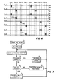
- the drive signals are alternating signal packets that differ from each other by being nonsynchronous and/or by being of opposing polarities if synchronous with each other. Referring to Figure 6, each signal packet contains sixteen cycles of an alternating signal that varies at a predetermined frequency.
- the different drive signals in combination include nonsynchronous sets of signal packet pairs, with the paired signal packets in each set being synchronous with each other, of approximately the same value, and of opposing polarities to thereby cause the amplitude of the sense signals derived in response to such synchronous pairs of drive signal packets to be low in relation to the variation in the amplitude of such sense signals resulting from the touch elements being touched by an operator.
- the signal packets of one polarity are referred to as drive signals DS; and the signal packets of the opposite polarity are referred to as inverted drive signals IDS.
- the term drive signal refers to whichever type of drive signal pattern (DS or IDS) is applied to the respective drive lines DL1-8.
- the drive signals are provided on the drive lines DL1-8 by the drive signal generator 17 in a repeating sequence of four different drive signal patterns DS P l, DSP2, DSP3 and DSP4.
- a drive signal DS is provided on drive line DL1
- an inverted drive signal IDS is provided on drive line DL3.
- Table 2 shows the association of the drive signals DS and the inverted drive signals IDS on the respective drive lines DL during the four different drive signal patterns DSPI-4.
- the paired drive signal DS and inverted drive signal ID S are synchronous with each other, of approximately the same value and of opposing polarities.
- the drive signal pattern information on lines 42 indicates the sequence in which the drive signal packets are placed upon given drive lines.
- Each of the drive lines DL1-8 is dedicated to receiving either drive signals DS or inverted drive signals IDS exclusively, as shown in Figure 6.
- the multiplexer 11 time-division multiplexes the eight different sense signals on sense lines SL1-8 to provide time-division multiplexed sense signals on line 43 to the amplifier 12.
- the amplifier 12 is a band pass amplifier centered at the predetermined frequency of the alternating signal within the signal packets of the drive signals.
- the synchronous demodulator frequency demodulates the signal on line 44 from the amplifier 12.
- the control logic circuit 16 controls the operation of the synchronous demodulator 13 by a signal on lines 45 to cause the demodulation of a signal packet on line 44 to be synchronous with the generation of the corresponding drive signal packet by the drive signal generator 17.
- the demodulated signals then are converted from analog signals to digital signals by the A/D converter 14 which provides a respective sense signal value (SSV) on lines 46 for the sense signal derived from one of the sense lines SL1-8 that is selected by the multiplexer 11 during one of drive patterns DSP1-4 ( Figure 6).
- the multiplexing rate is such that a sense signal from only one of the sense lines SL1-8 is provided on line 43 and subsequently demodulated during each occurrence of a drive signal pattern DSP.
- the sense signal values indicate both the amplitude and the polarity of the sense signals. Because opposing polarity drive signal patterns are provided, the number of sense signal values that must be processed to scan completely the array of touch elements is one-half the number of antenna lines. Thus, for this embodiment, only thirty-two sense signal values need be processed during each complete scan of the touch sensing array.
- Table 3 shows a processing sequence identification number for each of the sense signal values (SSV), and the sign under an appropriate convention of the variation in the sense signal value derived from each of the sense lines SL1-8 during each of the respective drive signal patterns DSP1-4 whenever a touch element is touched by an operator with respect to the antenna lines A that are connected to the touch element that is touched by the operator.
- a positive variation in the sense signal value is derived from sense line SL1 during DSPI and a negative variation in the sense signal value is derived from sense line SL4 during DSP4.
- the microprocessor 15 processes the sense signal values on lines 46 to provide information on lines 47 associated with any particular touch element that is touched by an operator.
- the touch element array 10 is used as a keyboard for a data processor 48. Accordingly, the information provided by the microprocessor on lines 47 constitutes a keyboard output signal to the data processor 48.
- the operation of the multiplexer 11 is controlled by signals provided on lines 49 by the microprocessor 15.
- the microprocessor also provides an initialization signal on line 50 to the control logic circuit 16, which coordinates the operation of the synchronous demodulator 13, the A/D converter 14 and the drive signal generator 17.
- the operation of the microprocessor 15 is reset by the data processor 48 by a signal on line 51.
- the microprocessor 15 is programmed to process the sense signal values (SSV) on lines 46 iteratively to ascertain the signs and values of the variations (SSVV) in the sense signal values (SSV) and to process the sense signal variation values (SSVV) to determine whether any such variation resulted from a touch element being touched by an operator.
- SSV sense signal values
- SSVV sense signal variation values
- the sense signal values are processed iteratively by comparing the sense signal values with baseline values derived from sense signal values provided when the touch element array is untouched by an operator to determine which one of three states is present.
- the first of the three states is an UNTOUCHED state.
- the second of the three states is a VALID TOUCH state in which a valid touch by an operator is present.
- the third of the three states is an INVALID RESPONSE state which occurs when neither the first state or the second state is present.
- step 0 represents a power on, reset operation; and in step 1, the variable values are initialized.
- step 2 a scan of the touch element array 10 is carried out iteratively with the production of sense signal values SSV1-32 as program input. Initial processing is carried out.
- step 3 a test is performed to determine if the sense signal variation values SSVVI-32 are all small. If so, the program branches to step 6 where the UNTOUCHED state is processed. If any of sense signal variation values SSVV1-32 is found not to be small in step 3, the program branches to step 4 where a test is performed to identify the presence or absence of the VALID TOUCH state.
- the VALID TOUCH state is processed in step 5. In the absence of the VALID TOUCH state the program branches from step 4 to step 7 where an INVALID RESPONSE is processed. Following each of steps 5, 6, or 7 there is a return to step 2.
- the initialization is shown in steps 1.1 and 1.2 to consist of inputting the sense signal values SSV1-32 and storing these values as baseline values BV1-32 and also as reserve values RV1-32.
- a baseline drift compensation count (BDCC) and a baseline revision count (BRC) are each initialized to 0.
- the microprocessor 15 is programmed to process the sense signal values (SSV) iteratively to determine whether any of the touch elements has been touched by an operator by comparing the sense signal values (SSV) with baseline values (BV) derived from sense signal values (SSV) provided when the touch elements are untouched by an operator to determine whether a sense signal variation value (SSVV) derived from such comparison exceeds a predetermined variation value bound (VVB); and to revise the baseline values (BV) in response to sensed variations in the sense signal values (SSV) over a predetermined number of iterations occurring in the absence of valid touch by an operator.
- the baseline values are revised in response to sensed variations in the sense signal values which are stable over a predetermined number of iterations and which indicate the INVALID RESPONSE state of the touch element array 10.
- the microprocessor 15 (a) stores a set of reserve values (RV) derived from a set including each of the respective sense signal values (S SV ); (b) iteratively compares each sense signal value (SSV) to each corresponding reserve value (RV); (c) revises the stored set of reserve values (RV) to correspond to a current set of sense signal values SSV1-32 whenever the difference between any sense signal value (SSV) and the corresponding reserve value (RV) exceeds a predetermined reserve value bound (RVB); (d) processes the sense signal variation values ( SS VV) derived from a current set of sense signal values SSV1-32 whenever any variation value (SSVV) derived from such set exceeds a variation value bound (VVB) to determine whether VVB was exceeded as a result of a touch element being touched by an operator; (e) increments a baseline revision count (BRC) in response to each current set of sense signal values SSV1-32 for which it is determined that
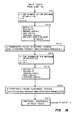
- Step (d) is shown in the flow chart of Figure 10 and steps (e) and (g) are shown in the flow chart of Figure 12. Accordingly, it is seen that the baseline values are revised to correspond to the reserve values when the INVALID RESPONSE state is present for a predetermined number of iterations during which time no revision of the reserve values occurs, no revision of baseline values to correspond to reserve values occurs and the VALID TOUCH state is not present. It is also seen that the baseline values are updated by either incrementing or decrementing each of the respective baseline values in accordance with whether the baseline value is less or greater than the respective last-provided sense signal value when the UNTOUCHED state is present for a predetermined number of consecutive iterations during which time no updating of the baseline values occurs.
- Sense signal values SSVl-32 are input in step 2.1.
- step 2.2 a test is done on the baseline revision count BRC.
- BRC baseline revision count
- each of the reserve values RV1-32 is altered as shown so as to become closer by 1 if possible to the respective value of SSV1-32.
- the SIGN function is employed in this step and in later steps in the usual way where the SIGN of a positive number is plus 1, the SIGN of 0 is 0, and the SIGN of a negative number is minus 1. This operation of step 2.4 is called reserve value drift compensation.
- step 2.3 Part of the significance of-this step 2.4 operation is shown by the test in step 2.3 where if any of the reserve values RV1-32 is found to depart by more than the reserve value bound RVB from the corresponding one of SSVl-32 there is a branch to step 2.5 where all of RV1-32 are given the respective values of the current SSVI-32 and where the baseline revision count (BRC) is reset to 0.
- step 2.6 the sense signal variation values SSVV1-32 are calculated as the respective differences of SSV1-32 and BV1-32.
- step 3.1 if the magnitude of each of SSVV1-32 is found to be smaller than the variation value bound VVB, the touch element array 10 is judged to be in the UNTOUCHED state and there is a branch to step 6. Otherwise there is a branch to step 4.
- the microprocessor 15 determines whether the maximum variation value (ROWMAX) derived from the row antenna lines Al-32 exceeds a predetermined threshold value (THR); (b) determines whether none of the other variation values (SSVV) derived from the row antenna lines Al-32 exceeds a tolerance value (TOL) that is a predetermined fraction of the maximum variation value (ROWMAX) derived from the row antenna lines Al-32; (c) determines whether the maximum variation value (COLMAX) derived from the column antenna lines A33-64 exceeds the predetermined threshold value (THR); and (d) determines whether none of the other variation values (SSVV) derived from the column antenna lines A33-64 exceeds a tolerance value (TOL) that is a predetermined fraction of the maximum variation value (COLMAX) derived from the column antenna lines A33-64.
- TOL tolerance value
- Tests for a valid touch response are carried out in steps 4.1 through 4.6.
- the variable ROWMAX is always assigned the value of the largest magnitude of the current set of sense signal variation values SSVVI-16 derived from the row antenna lines Al-32.
- ROWMAX is compared to the predetermined threshold value THR. If ROWMAX exceeds THR there is a branch to step 4.2 where the tolerance value TOL is set to some fixed fraction of the value of ROWMAX.
- each of the magnitudes of SSVV1-16 other than the one chosen as ROWMAX is compared to TOL.
- a VALID ROW TOUCH response is judged to be present and the program branches to step 4.4 where the largest magnitude (COLMAX) of the current set of sense signal value variations SSVV17-32 derived from the column antenna lines A33-64 is determined. COLMAX is compared to the threshold value THR. If COLMAX exceeds THR, then TOL is recalculated as a fixed fraction of COLMAX in step 4.5; and in step 4.6, each of the magnitudes of S S VV17-32 other than the one chosen as COLMAX is compared to TOL.
- step 5.1 which begins the processing of a valid touch, the counts BDCC and BRC are each reset to 0. The significance of these resets will be appreciated when the program flow charts shown in Figures 11 and 12 are described.
- step 5.2 further processing of a VALID TOUCH response is carried out including the appropriate encoding of the touched touch element by row number and by column number which numbers may be calculated using the information in Table 3.
- the microprocessor 15 is further programmed to compensate for drift in the sense signal values (SSV) that are provided when the touch elements are in the untouched state.
- the microprocessor 15 increments the baseline drift compensation count (BDCC) in response to each current set of sense signal values SSVI-32 for which there is no sense signal variation value (SSVV) that exceeds the variation value bound (VVB);
- BDCCL predetermined compensation count limit
- step 6.1 the baseline drift compensation count BDCC is incremented by two counts.
- step 6.2 BDCC is compared to the predetermined compensation count limit BDCCL. If BDCC has reached or exceeded BDCCL, there is a branch to step 6.3 where BDCC is reset to 0.
- step 6.4 each of the baseline values BV1-32 is altered as shown so as to become closer by 1 if possible to the respective value of the current sense signal values SSVI-32.
- the process of compensating for baseline value drift further includes decrementing the baseline drift compensation count (BDCC) to not less than zero in response to each current set of sense signal values SSVI-32 for which a sense signal variation value(SSVV) exceeds the predetermined variation value bound (VVB) except when it is determined that the exceeding of VVB was the result of a touch element being touched by an operator.
- BDCC baseline drift compensation count
- VVB predetermined variation value bound
- step 7.4 If there is equality there is a branch to step 7.4 where the baseline values BV1-32 are assigned the respective reserve values RV1-32, as discussed above in relation to the description of the program flow chart shown in Figure 9. Further processing of the INVALID RESPONSE state is carried out in step 7.3 as needed.
- baseline value drift compensation occurs in step 6, where the UNTOUCHED state is processed, when BDCC reaches BDCCL.
- BDCC is reset to 0 in step 5, incremented by 2 in step 6, and is decremented by 1 if positive in step 7. Since there is passage through only one of steps 5, 6, or 7 during each iteration (which corresponds to a sequence in which each of drive signal patterns DSPl-4 is repeated for each of the sense lines SLI-8), the condition which brings about baseline value drift compensation is apparent.
- complete baseline revision with the resulting replacement of BV1-32 by RV1-32 occurs in step 7, where the INVALID RESPONSE state is processed, when BRC reaches BRCL.
- BRC is incremented in step 7, is reset to 0 in step 5, and is possibly reset to 0 in step 2.
- the conditions needed for complete baseline value revision are apparent: first, sufficient stability of SSV1-32 so that the resetting of BRC is avoided in step 2, and second, passage through step 7 BRCL times before passing through step 5.
- THR may be set equal to 8.
- RVB and VVB may be set equal to 4.
- BDCCL may be chosen so that baseline value drift compensation occurs at the rate of 1 per second when all SSVs are consistently less than or equal to VVB in magnitude.
- TOL may be assigned the value of ROWMAX/4 and in step 4.5 TOL may be assigned the value of COLMAX/4.
- BRCL may be chosen so that a complete baseline value revision occurs after 2 seconds of stabilized SSVs in the INVALID RESPONSE state.
- the preselected values of BRC which lead to a branch to reserve value drift compensation from step 2.2 in the process of Figure 9 may be chosen as 1, 2, 4, 8, ... up to BRCL.
- the touch element array 10 is adapted so that instead of the touch elements respectively serving as keys of a keyboard, the touch elements are dimensioned and disposed so that an operator firmly touching an interior touch element of the array with his finger necessarily touches a plurality of touch elements simultaneously.
- the microprocessor 15 is programmed to respond to the sense signal values produced upon a plurality of the touch elements being touched simultaneously so as to provide an output indication of the coordinate position on the touch element array 10 that is touched by the operator.
- the indication of the position of finger touch may be used in a variety of control situations, such as, for example, selecting the cursor position on a cathode ray tube constituting the display portion of a computer terminal.
- transparent conductive material may be used for the antenna lines and the touch elements and the touch element array may overlay the cathode tube.
- each touch element TE is connected to only a single antenna line A. All of the row antenna lines Al, ... are supported on one side of a thin dielectric substrate, and all of the column antenna lines A33, ... are supported on the opposite side of said substrate.
- Each touch element TE includes only one conductive tab 53.
- the center line-to-center line distance D between the row antenna lines A1, ... is 0.25 inch.
- the column antenna lines A 33, ... are separated by the same distance.
- the touch elements are square in shape and extend from their respective antenna lines which traverse the touch elements diagonally. Each square has a diagonal dimension of 0.2 inch.
- the touch elements on one side of the substrate do not underlie the touch elements on the opposite side of the substrate. Instead, as shown in Figure 13, the touch elements on one side of the substrate are disposed symmetrically between the positions of the touch elements on the opposite side of the substrate.
- the touch element array of this alternative embodiment has the same basic monolithic construction as described above for the touch elements shown in Figure 4, except that the tabs 20 and 21 on opposite sides of the substrate 22 constitute separate touch elements in the embodiment of Figure 13. Also the protective film 25 ordinarily would not be backprinted with indicia to show the outline of each touch element. The use of the optional overlay 27 would be appropriate with this embodiment when it is desired to specify portions of the array as having particular significance.
- the entire touch array 10 in this alternative preferred embodiment is a part of a monolithic construction that also includes the drive line-to-antenna capacitors DLACI-64 and the antenna-to-sense line capacitors ASLCI-64 as described above with reference to Figure 5.
- FIG. 14 An alternative monolithic construction of the touch element array of Figure 13 in combination with the drive line-to-antenna capacitors D LACl-64 and the antenna-to-sense line capacitors ASLCl-64 is shown in Figures 14 and 15.
- a row antenna line 54 of the array of row antenna lines Al-32 is supported by the top side of a first thin dielectric Mylar film substrate 55; and a column antenna line 56 of the array of column antenna lines A33-64 is supported by the bottom side of the first substrate 55.
- the drive lines and sense lines are supported by opposite sides of a second thin dielectric Mylar film substrate 57.
- a line 58 of either the array of row drive lines DL1-4 or the array of sense lines SL1-8 is supported by the top side of the second substrate 57; and a line 59 of either the array of column drive lines DL5-8 or the array of sense lines SL1-8 is supported by the bottom side of the second substrate 57.
- a third thin dielectric Mylar film substrate 60 separates the first substrate 55 and the second substrate 57. Each of these three substrates is approximately 0.001 inch thick.
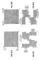
- Figures 15A, 15B, 15C and 15D show the respective layers of the arrays containing the lines 54, 56, 58 and 59 shown in Figure 14.
- the registration marks in these figures indicate the alignment of the respective layers.
- the top layer, shown in Figure 15A contains the array of row antenna lines Al-32.
- the next layer, shown in Figure 15B contains the array of column antenna lines A33-64.
- the following layer, shown in Figure 15C contains the array of row drive lines DLI-4 and portions of the array of sense lines SL1-8.
- the bottom layer, shown in Figure 15D contains the array of column drive lines DL5-8 and portions of the array of sense lines SL1-8.
- each of the row antenna lines Al-32 is capacitively coupled primarily to one of the row drive lines DL1-4 and to one of the sense lines SL1-8; and each of the column antenna lines A33-64 is capacitively coupled primarily to one of the column drive lines DL5-8 and to one of the sense lines SL1-8.
- the second substrate 57 is supported by a nonconductive mechanical support layer 61, which is covered on its bottom side by a grounded thin conductive, electrically shielding layer 62.
- the touch element array further includes a protective 0.005 inch Lexan plastic film layer 63 covering the top unsupported side of the first substrate 55.
- the touch element array may also include a paper overlay layer 64 having various indicia and/or patterns thereon to particularly indicate specific portions of the array.
- the microprocessor program for this alternative embodiment necessarily is modified in steps 4.3 and 4.6 to accommodate the fact that more than one touch element connected to the row antenna lines Al-32 and more than one touch element connected to the column antenna lines A33-64 may be touched during a valid touch.
- the program can be modified to exempt from the tolerance test the sense signal value variations (SSVV) derived from the two antenna lines on either side of the respective antenna lines from which ROWMAX and COLMAX are derived.
- SSVV sense signal value variations
- the interpolation routine for estimating the y coordinate of operator finger touch position from ARVV1-32 is set forth in step 5.2.1 through 5.2.3
- the interpolation process for estimating the x coordinate of operator touch position from ARVV33-64 is set forth in steps 5.2.4 through 5.2.6.
- steps 5.2.4 through 5.2.6 are to be considered as an expansion in this preferred embodiment of step 5.2 of the process covered by the flow chart of Figure 10 for the first described preferred embodiment.
- These interpolation processes produce x and y coordinates which indicate the position of operator finger touch. Each coordinate is a number between 1 and 125.
- step 5.2.1 the variable k is assigned the number of the maximum of ARVV1-32; the variable j is assigned the value of k-1; and the variable m is assigned the value of k+1.
- a variable called ARVVO is assigned the value 0 and ARVV33 is temporarily assigned the value 0.
- variables PREMAX, MAX, and POSTMAX are assigned the respective values ARVVj, ARVVk, and ARVVm. Following this, the value of ARVV33 is restored to the value of the positive part of SSVV17.
- step 5.2.3 the variable Y-COORDINATE is calculated from the elementary interpolation formula:
- a further modification of the microprocessor program for this alternative embodiment is to exempt from the tolerance test of steps 4.3 and 4.6 described in relation to the flow chart of Figure 10, the antenna referred variation values (ARVV) derived from the two adjacent antenna lines on each side of the antenna line associated with the maximum ARVV.
- the ARVVs correspond to the SSVVs in Figure 10.
- each touch element includes conductive tabs 20 and 21 extending respectively from a row antenna line Al-32 and a column antenna line A33-64.
- This encoding principle clearly could be extended so that the antenna lines could be divided into three or more groups and that finger contact with a touch element would result in an increase in the variable capacitance to ground of an antenna line from each of the three or more groups.
- FIG 4 a cross-sectional view of a touch element is shown. It is apparent that, in areas other than under the tabs 20 and 21, the thin film substrate 22 need not remain close to the surface of the touch element and could be covered by some of the supporting layer 23. In some applications this might be desired as a device to protect portions of the antenna lines not underlying the tabs 20, 21 from being affected by touch.
- the drive signal patterns shown in Figure 6 illustrate a technique of achieving a balancing of drive signals by the simultaneous use of drive signals D S and inverted drive signals IDS on a pair of drive lines. It is apparent that other means of balancing could be found which avoid placing a drive signal on more than one drive line at a time and thus avoid having a simultaneous increase in the variable capacitance to ground (VCG) of two antenna lines go undetected such as the simultaneous increase in the VCG of antenna lines Al and A3 as is apparent upon referring to Table 3.
- VCG variable capacitance to ground
- a drive signal D S is provided on drive line DL1 and an inverted drive signal IDS is provided on drive line DL3.
- TABLE 4 shows the association of the drive signals DS, the inverted drive signals IDS and the drive lines DL during the six different drive signal patterns DSP.
- the paired drive signal DS and inverted drive signal IDS are synchronous with each other, of approximately the same value and of opposing polarities.
- a plurality of the drive signal packets, DS, I D S are applied sequentially on some of the drive lines and are paired synchronously with the drive signal packets of opposite polarity IDS, DS on different ones of the other drive lines.
- drive signal packets DS are applied on drive line DL1 during sequential drive signal patterns DSP1 and DSP3 and are paired synchronously with inverted drive signals on drive lines DL3 and DL4 during drive signal patterns DSP1 and DSP3 respectively.
- a total of forty- eight different sense signal values SSV are derived from the eight sense lines SL1-8 and provided on lines 46 to the microprocessor 15.
- Table 5 shows the sign under the sign convention of Table 3 of the variation of the respective sense signal values S SV associated with the different antenna lines A that is due to the onset of an operator touching a touch element connected to the respective antenna lines.
- the SSV number is a processing sequence identification number and not the value of the sense signal.
- the microprocessor 15 is programmed to process the sense signal values SSV1-48 on line 43 iteratively to ascertain the signs and values of the variations (SSVV) in the sense signal values (SSV) and to process the sense signal variation values (SSVV) to determine whether such variation resulted from a touch element being touched by an operator.
- SSVV sense signal variation values
- step 2 a scan of the touch element array 10 is carried out iteratively with the production of sense signal values SSV1-48 as the program input.
- Significant program differences are shown in the flow charts of Figures 18 and 19.
- the step-numbering system in Figures 18 and 19 agrees in the first digit with that of Figure 7.
- step 1.1 consists of initializing accumulated difference values AD1-48 to zero and a stability count SC to zero.
- Sense signal values SSV1-48 are input in step 2.1.
- step 2.2 the sense signal variation value (SSVV) is calculated for each 1 ⁇ k ⁇ 48 and is added to ADk. The previous sense signal value (SSVk) is then discarded and the current sense signal value of SSVk is saved.
- step 2.3 a stability count SC is incremented if the magnitude of each SSVVk is found to be less than a predetermined stability bound SB for 1 ⁇ k S 48.
- step 2.4 the stability count SC is compared to a predetermined count limit SCL. If there is equality there is a branch to step 2.5 where the accumulated difference values AD1-48 and the stability count SC are reset to zero. Otherwise there is a branch to step 3.1.
- step 3.1 if the magnitude of each accumulated difference value ADl-48 is found to be smaller than a predetermined accumulated difference bound ADB, the touch element array is judged to be in the UNTOUCHED state and there is a branch to step 6, otherwise there is a branch to step 4.
- the current sense signal values SSV1-48 are compared with the respective sense signal values during the previous iteration to determine sense signal variation values SSVVl-48.
- the sense signal variation values are added to the respective accumulated difference values AD1-48 for each sense signal; and each of the accumulated difference values ADI-48 is compared to a predetermined accumulated difference bound ADB to determine whether the UNTOUCHED state is present.
- the accumulated difference values ADl-48 are reset to an initial value of zero when each of the sense signal variation values SSVV1-48 remain less than a predetermined stability bound SB over a predetermined number of iterations SCL.
- Each of the sense signal variation values SSVV1-48 is compared to SB; and the stability count SC is incremented in response to each set of sense signal values SSV1-48 for which none of the sense signal variation values SSVV1-48 exceeds the predetermined stability bound SB.
- the accumulated difference values ADl-48 and the stability count SC are reset to an initial value of zero when the stability count SC reaches the predetermined count limit SCL.
- the microprocessor 15 determines (a) ROWMAX1, the maximum magnitude of the accumulated differences ADl-24 which are the differences derived from the row antenna lines Al-32; (b) ROWMAX2, the second largest magnitude of ADI-24; (c) TOLI, a tolerance value which is a predetermined fraction of ROWMAXI; and (d) THR2, a predetermined fraction of ROWMAXI which serves as a threshold value for ROWMAX2.
- the microprocessor 15 further determines (e) COLMAX1, the maximum magnitude of the accumulated differences AD25-48 which are the differences derived from the column antenna lines A33-64; (f) COLMAX2, the second largest magnitude of AD25-48; (g) TOL2, a tolerance value which is a predetermined fraction of COLMAX1; and (h) THR4, a predetermined fraction of COLMAX1 which serves as a threshold value for COLMAX2.
- a valid touch onset is judged to be present when separate determinations relating to row antennas Al-32 and to column antennas A33-64 are affirmative.
- Determinations related to row antennas Al-32 are that (i) ROWMAX1 must exceed a predetermined threshold value THR1; (j) if ROWMAX1 is derived from a row antenna line to which two drive signal packets are applied during each repetitive sequence of drive signal patterns DSP1-6, then ROWMAX2 must exceed the threshold THR2; (k) all magnitudes of the accumulated differences AD1-24 other than ROWMAXI, and when applicable ROWMAX2, must be less than TOL1; and (1) the specific one of ADl-24 giving rise to ROWMAXl, and when applicable the specific one of ADl-24 giving rise to ROWMAX2, must indicate, on consulting Table 5 (which is stored in the memory of the microprocessor 15), an appropriate response as concerns row antennas to the onset of touch of a single touch element.
- Determinations related to column antennas A33-64 are that (m) COLMAX1 must exceed a predetermined threshold value THR3; (n) if COLMAX1 is derived from a column antenna line to which two drive signal packets are applied during each repetitive sequence of drive signal patterns DSP1-6, then COLMAX2 must exceed the threshold THR4; (o) all magnitudes of the accumulated differences AD25-48 other than COLMAXl, and when applicable COLMAX2, must be less than TOL2; and (p) the specific one of AD25-48 giving rise to COLMAX1, and when applicable the specific one of AD25-48 giving rise to COLMAX2, must indicate, on consulting Table 5, an appropriate response as concerns column antennas to the onset of touch of a single touch element.
- Tests for a valid touch response are carried out in steps 4.1 through 4.14, as shown in the flow chart of Figure 19.
- step 4.1 ROWMAX1 is compared to the first predetermined threshold value THR1. If ROWMAX1 exceeds THR1 there is a branch to step 4.2 where the tolerance value TOLl is set to some fixed fraction of the value of ROWMAX1.
- step 4.3 if it is determined that ROWMAXI is derived from a row antenna line to which two drive signal packets are applied during each repetitive sequence of drive signal patterns DSPI-6, whereby a valid touch response requires that the second largest magnitude of the accumulated difference values AD1-24, ROWMAX2, be over the threshold value THR2, there is a branch to step 4.5.
- step 4.4 each of the accumulated difference values AD1-24 other than the one chosen as ROWMAX1 is compared to the tolerance value TOL1. If none of these values exceeds TOL1 then the program branches to step 4.7.
- ROWMAX2 is compared to the threshold value THR2. If ROWMAX2 is found to be greater than THR2 there is a branch to step 4.6 where each of the accumulated difference values ADI-24 other than the ones chosen as ROWMAX1 and ROWMAX2 is compared to TOL1. If none of these values exceeds TOL1 there is a branch to step 4.7 where the accumulated difference associated with ROWMAX1 and when applicable the accumulated difference associated with ROWMAX2 are checked using the information in Table 5. If the result is found to be valid, then a VALID ROW TOUCH is judged to be present and the program branches to step 4.8.
- step 4.8 the variable COLMAX1 is compared to the threshold value THR3. If COLMAX1 exceeds THR3 then TOL2 is calculated as a fixed fraction of COLMAX1 in step 4.9.
- step 4.10 if it is determined that COLMAX1 is derived from a column antenna line to which two drive signal packets are applied during each repetitive sequence of drive signal patterns DSPl-6, whereby a valid touch response requires that the second largest of the accumulated difference values AD25-48, COLMAX2, be over the threshold value THR2, there is a branch to step 4.12. Otherwise there is a branch to step 4.11 where each of the accumulated difference values AD25-48 other than the one chosen as COLMAX1 is compared to the tolerance value TOL2.
- step 4.14 COLMAX2 is compared to the threshold value THR4. If COLMAX2 is found to be greater than THR4, there is a branch to step 4.13 where each of the accumulated difference values AD25-48 other than the ones chosen as COLMAX1 and COLMAX2 is compared to TOL2. If none of these values exceeds TOL2, there is a branch to step 4.14 where the accumulated difference associated with COLMAX1 and when applicable the accumulated difference associated with COLMAX2 are checked using the information in Table5. If the result is found to bevalid,then the tests for a VALID TOUCH have been passed and there is an exit to step 5.1.
- step 5.1 processing of a VALID TOUCH response is carried out including the appropriate encoding of the touched touch element by row number and by column number which numbers may be calculated using the information in Table 5.
- THR1 and THR3 may be set equal to 8.
- SCL may be chosen so that the accumulated differences AD are reset to 0 after 0.5 seconds of stable operation.
- TOL1 may be assigned the value of ROWMAX1/4 and step 4.9 TOL2 may be assigned the value of COLMAXI/4.
- THR2 may be assigned the value of ROWMAXl/2 and in step 4.12 THR4 may be assigned the value of COLMAX1/2.
- the accumulated difference values AD1-48 may be reset to zero when operator touch of a touch element is present for an extended dwell time without danger of misinterpretation of the subsequent accumulated difference values ADl-48 that occur when operator touch is removed from the touch element. This is in contrast to the situation described above in conjunction with the first-described preferred embodiment discussed in relation to Figures 6-12, where resetting baseline values (BV) during touch is prohibited since misinterpretation of the cessation of touch would then occur.
- BV baseline values
Landscapes
- Engineering & Computer Science (AREA)
- General Engineering & Computer Science (AREA)
- Theoretical Computer Science (AREA)
- Human Computer Interaction (AREA)
- Physics & Mathematics (AREA)
- General Physics & Mathematics (AREA)
- Electronic Switches (AREA)
- Measurement Of Length, Angles, Or The Like Using Electric Or Magnetic Means (AREA)
- Measuring Fluid Pressure (AREA)
Priority Applications (1)
| Application Number | Priority Date | Filing Date | Title |
|---|---|---|---|
| AT84115648T ATE45254T1 (de) | 1983-12-27 | 1984-12-17 | System mit einer beruehrungsempfindlichen, auf kapazitaetsaenderungen ansprechenden anordnung. |
Applications Claiming Priority (2)
| Application Number | Priority Date | Filing Date | Title |
|---|---|---|---|
| US56604583A | 1983-12-27 | 1983-12-27 | |
| US566045 | 1983-12-27 |
Publications (2)
| Publication Number | Publication Date |
|---|---|
| EP0150421A1 true EP0150421A1 (fr) | 1985-08-07 |
| EP0150421B1 EP0150421B1 (fr) | 1989-08-02 |
Family
ID=24261231
Family Applications (1)
| Application Number | Title | Priority Date | Filing Date |
|---|---|---|---|
| EP84115648A Expired EP0150421B1 (fr) | 1983-12-27 | 1984-12-17 | Système à tableau sensible au toucher et aux variations de capacité |
Country Status (4)
| Country | Link |
|---|---|
| EP (1) | EP0150421B1 (fr) |
| JP (1) | JPS60158721A (fr) |
| AT (1) | ATE45254T1 (fr) |
| DE (1) | DE3479276D1 (fr) |
Cited By (7)
| Publication number | Priority date | Publication date | Assignee | Title |
|---|---|---|---|---|
| WO1988005577A1 (fr) * | 1987-01-15 | 1988-07-28 | Ronald Peter Binstead | Ameliorations apportees aux systemes de touches de claviers numeriques ou en rapport avec ces systemes |
| EP0444919A1 (fr) * | 1990-03-02 | 1991-09-04 | The Board Of Trustees Of The Leland Stanford Junior University | Bâton agissant en trois dimensions et détecteur de mouvement |
| FR2662528A1 (fr) * | 1990-05-25 | 1991-11-29 | Sextant Avionique | Dispositif pour la localisation d'un objet situe a proximite d'une aire de detection et clavier transparent utilisant ledit dispositif. |
| WO1995016308A1 (fr) * | 1993-12-08 | 1995-06-15 | Fafalios Stamos Anastasios Dim | Commutateur electronique tactile et clavier comprenant ce commutateur |
| EP0688102A1 (fr) * | 1994-06-09 | 1995-12-20 | Whirlpool Europe B.V. | Dispositif de commande comportant une touche tactile à haute fréquence pour des appareils électroménagers comme des fours, des plaques de cuisson, machines à laver, lave-vaisselle, ou similaire |
| EP0917291A3 (fr) * | 1995-01-20 | 2001-01-10 | Dynapro Systems, Inc. | Capteur à effleurement capacitif |
| US9395857B2 (en) | 2007-12-24 | 2016-07-19 | Tpk Holding Co., Ltd. | Capacitive touch panel |
Families Citing this family (2)
| Publication number | Priority date | Publication date | Assignee | Title |
|---|---|---|---|---|
| KR100927064B1 (ko) * | 2004-08-16 | 2009-11-13 | 애플 인크. | 터치 감지 장치의 공간 해상도를 증가시키는 방법 |
| DE102010040434B4 (de) * | 2010-09-08 | 2020-01-30 | BSH Hausgeräte GmbH | Kapazitive Bedieneinrichtung für ein Haushaltsgerät, Haushaltsgerät und Verfahren zum Betreiben einer kapazitiven Bedieneinrichtung in einem Haushaltsgerät |
Citations (6)
| Publication number | Priority date | Publication date | Assignee | Title |
|---|---|---|---|---|
| US4145748A (en) * | 1977-12-23 | 1979-03-20 | General Electric Company | Self-optimizing touch pad sensor circuit |
| US4186392A (en) * | 1978-07-28 | 1980-01-29 | Burroughs Corporation | Touch panel and operating system |
| US4233522A (en) * | 1978-10-30 | 1980-11-11 | General Electric Company | Capacitive touch switch array |
| US4281323A (en) * | 1978-12-05 | 1981-07-28 | Bank Computer Network Corporation | Noise responsive data input apparatus and method |
| US4290052A (en) * | 1979-10-26 | 1981-09-15 | General Electric Company | Capacitive touch entry apparatus having high degree of personal safety |
| US4305135A (en) * | 1979-07-30 | 1981-12-08 | International Business Machines Corp. | Program controlled capacitive keyboard variable threshold sensing system |
Family Cites Families (3)
| Publication number | Priority date | Publication date | Assignee | Title |
|---|---|---|---|---|
| GB2022264A (en) * | 1978-05-22 | 1979-12-12 | Gen Electric | High density capacitive touch switch array arrangement |
| JPS5923410B2 (ja) * | 1978-06-09 | 1984-06-01 | パナフアコム株式会社 | タツチキ−ボ−ド |
| JPS5887725A (ja) * | 1981-11-18 | 1983-05-25 | 富士通株式会社 | 座標検出装置 |
-
1984
- 1984-12-17 DE DE8484115648T patent/DE3479276D1/de not_active Expired
- 1984-12-17 EP EP84115648A patent/EP0150421B1/fr not_active Expired
- 1984-12-17 AT AT84115648T patent/ATE45254T1/de not_active IP Right Cessation
- 1984-12-27 JP JP59274263A patent/JPS60158721A/ja active Pending
Patent Citations (6)
| Publication number | Priority date | Publication date | Assignee | Title |
|---|---|---|---|---|
| US4145748A (en) * | 1977-12-23 | 1979-03-20 | General Electric Company | Self-optimizing touch pad sensor circuit |
| US4186392A (en) * | 1978-07-28 | 1980-01-29 | Burroughs Corporation | Touch panel and operating system |
| US4233522A (en) * | 1978-10-30 | 1980-11-11 | General Electric Company | Capacitive touch switch array |
| US4281323A (en) * | 1978-12-05 | 1981-07-28 | Bank Computer Network Corporation | Noise responsive data input apparatus and method |
| US4305135A (en) * | 1979-07-30 | 1981-12-08 | International Business Machines Corp. | Program controlled capacitive keyboard variable threshold sensing system |
| US4290052A (en) * | 1979-10-26 | 1981-09-15 | General Electric Company | Capacitive touch entry apparatus having high degree of personal safety |
Non-Patent Citations (1)
| Title |
|---|
| PATENT ABSTRACTS OF JAPAN, vol. 7, no. 182, 11th August 1983, page (E-192) (1327); & JP-A-58 085636 (CASIO KEISANKI K.K.) 23-05-1983 * |
Cited By (8)
| Publication number | Priority date | Publication date | Assignee | Title |
|---|---|---|---|---|
| WO1988005577A1 (fr) * | 1987-01-15 | 1988-07-28 | Ronald Peter Binstead | Ameliorations apportees aux systemes de touches de claviers numeriques ou en rapport avec ces systemes |
| GB2223986A (en) * | 1987-01-15 | 1990-04-25 | Ronald Peter Binstead | Improvements in or relating to touch keypad systems |
| EP0444919A1 (fr) * | 1990-03-02 | 1991-09-04 | The Board Of Trustees Of The Leland Stanford Junior University | Bâton agissant en trois dimensions et détecteur de mouvement |
| FR2662528A1 (fr) * | 1990-05-25 | 1991-11-29 | Sextant Avionique | Dispositif pour la localisation d'un objet situe a proximite d'une aire de detection et clavier transparent utilisant ledit dispositif. |
| WO1995016308A1 (fr) * | 1993-12-08 | 1995-06-15 | Fafalios Stamos Anastasios Dim | Commutateur electronique tactile et clavier comprenant ce commutateur |
| EP0688102A1 (fr) * | 1994-06-09 | 1995-12-20 | Whirlpool Europe B.V. | Dispositif de commande comportant une touche tactile à haute fréquence pour des appareils électroménagers comme des fours, des plaques de cuisson, machines à laver, lave-vaisselle, ou similaire |
| EP0917291A3 (fr) * | 1995-01-20 | 2001-01-10 | Dynapro Systems, Inc. | Capteur à effleurement capacitif |
| US9395857B2 (en) | 2007-12-24 | 2016-07-19 | Tpk Holding Co., Ltd. | Capacitive touch panel |
Also Published As
| Publication number | Publication date |
|---|---|
| DE3479276D1 (en) | 1989-09-07 |
| ATE45254T1 (de) | 1989-08-15 |
| EP0150421B1 (fr) | 1989-08-02 |
| JPS60158721A (ja) | 1985-08-20 |
Similar Documents
| Publication | Publication Date | Title |
|---|---|---|
| US4733222A (en) | Capacitance-variation-sensitive touch sensing array system | |
| US4420744A (en) | Keyboard crosspoint encoder having N-key rollover | |
| US4233522A (en) | Capacitive touch switch array | |
| EP0097498B1 (fr) | Dispositif sensible à l'effleurement | |
| US3974332A (en) | Tablet for use in a coordinate digitizer | |
| US3399401A (en) | Digital computer and graphic input system | |
| US4952757A (en) | Low-power electromagnetic digitizer tablet | |
| US5933102A (en) | Capacitive sensitive switch method and system | |
| EP0513870B1 (fr) | Tablette pour entrer des informations dans un ordinateur | |
| US4686332A (en) | Combined finger touch and stylus detection system for use on the viewing surface of a visual display device | |
| US5801682A (en) | Tactile designation device with high-resolution transparent capacitive surface | |
| US5563381A (en) | Handwriting capture system with segmented digitizer | |
| EP2503433B1 (fr) | Dispositif de détection tactile et son procédé de balayage | |
| EP0186464B1 (fr) | Capteur tactile électrographique | |
| US9035903B2 (en) | Touch sensor | |
| US6373475B1 (en) | Converter for resistive touchscreens | |
| US3999012A (en) | Graphic entry tablet with improved addressing | |
| EP3291067B1 (fr) | Dispositif d'entrée à commande tactile et dispositif d'affichage tactile | |
| US4456787A (en) | Electrographic system and method | |
| EP0093565B1 (fr) | Dispositif sensible à l'effleurement | |
| US3992579A (en) | Tablet system with digital activation | |
| EP0150421B1 (fr) | Système à tableau sensible au toucher et aux variations de capacité | |
| EP3951566A1 (fr) | Substrat de commande tactile, dispositif de commande tactile et procédé de détection commande tactile | |
| US5051545A (en) | Digitizer with serpentine conductor grid having non-uniform repeat increment | |
| JP2015122067A (ja) | 制御点検知パネル、及び当該制御点検知パネルのデザイン方法 |
Legal Events
| Date | Code | Title | Description |
|---|---|---|---|
| PUAI | Public reference made under article 153(3) epc to a published international application that has entered the european phase |
Free format text: ORIGINAL CODE: 0009012 |
|
| AK | Designated contracting states |
Designated state(s): AT BE CH DE FR GB IT LI LU NL SE |
|
| 17P | Request for examination filed |
Effective date: 19850627 |
|
| 17Q | First examination report despatched |
Effective date: 19860821 |
|
| R17C | First examination report despatched (corrected) |
Effective date: 19870331 |
|
| GRAA | (expected) grant |
Free format text: ORIGINAL CODE: 0009210 |
|
| AK | Designated contracting states |
Kind code of ref document: B1 Designated state(s): AT BE CH DE FR GB IT LI LU NL SE |
|
| PG25 | Lapsed in a contracting state [announced via postgrant information from national office to epo] |
Ref country code: SE Effective date: 19890802 Ref country code: NL Effective date: 19890802 Ref country code: LI Effective date: 19890802 Ref country code: IT Free format text: LAPSE BECAUSE OF FAILURE TO SUBMIT A TRANSLATION OF THE DESCRIPTION OR TO PAY THE FEE WITHIN THE PRESCRIBED TIME-LIMIT;WARNING: LAPSES OF ITALIAN PATENTS WITH EFFECTIVE DATE BEFORE 2007 MAY HAVE OCCURRED AT ANY TIME BEFORE 2007. THE CORRECT EFFECTIVE DATE MAY BE DIFFERENT FROM THE ONE RECORDED. Effective date: 19890802 Ref country code: CH Effective date: 19890802 Ref country code: BE Effective date: 19890802 Ref country code: AT Effective date: 19890802 |
|
| REF | Corresponds to: |
Ref document number: 45254 Country of ref document: AT Date of ref document: 19890815 Kind code of ref document: T |
|
| REF | Corresponds to: |
Ref document number: 3479276 Country of ref document: DE Date of ref document: 19890907 |
|
| REG | Reference to a national code |
Ref country code: CH Ref legal event code: PL |
|
| ET | Fr: translation filed | ||
| PG25 | Lapsed in a contracting state [announced via postgrant information from national office to epo] |
Ref country code: LU Free format text: LAPSE BECAUSE OF NON-PAYMENT OF DUE FEES Effective date: 19891231 |
|
| NLV1 | Nl: lapsed or annulled due to failure to fulfill the requirements of art. 29p and 29m of the patents act | ||
| PLBE | No opposition filed within time limit |
Free format text: ORIGINAL CODE: 0009261 |
|
| STAA | Information on the status of an ep patent application or granted ep patent |
Free format text: STATUS: NO OPPOSITION FILED WITHIN TIME LIMIT |
|
| 26N | No opposition filed | ||
| PGFP | Annual fee paid to national office [announced via postgrant information from national office to epo] |
Ref country code: FR Payment date: 20001115 Year of fee payment: 17 |
|
| PGFP | Annual fee paid to national office [announced via postgrant information from national office to epo] |
Ref country code: GB Payment date: 20001208 Year of fee payment: 17 |
|
| PGFP | Annual fee paid to national office [announced via postgrant information from national office to epo] |
Ref country code: DE Payment date: 20010228 Year of fee payment: 17 |
|
| PG25 | Lapsed in a contracting state [announced via postgrant information from national office to epo] |
Ref country code: GB Free format text: LAPSE BECAUSE OF NON-PAYMENT OF DUE FEES Effective date: 20011217 |
|
| REG | Reference to a national code |
Ref country code: GB Ref legal event code: IF02 |
|
| PG25 | Lapsed in a contracting state [announced via postgrant information from national office to epo] |
Ref country code: DE Free format text: LAPSE BECAUSE OF NON-PAYMENT OF DUE FEES Effective date: 20020702 |
|
| GBPC | Gb: european patent ceased through non-payment of renewal fee |
Effective date: 20011217 |
|
| PG25 | Lapsed in a contracting state [announced via postgrant information from national office to epo] |
Ref country code: FR Free format text: LAPSE BECAUSE OF NON-PAYMENT OF DUE FEES Effective date: 20020830 |
|
| REG | Reference to a national code |
Ref country code: FR Ref legal event code: ST |