EP0153251A1 - Bildaufnahmevorrichtung mit stabförmiger multilinearer Ladungsverschiebungsanordnung - Google Patents
Bildaufnahmevorrichtung mit stabförmiger multilinearer Ladungsverschiebungsanordnung Download PDFInfo
- Publication number
- EP0153251A1 EP0153251A1 EP85400279A EP85400279A EP0153251A1 EP 0153251 A1 EP0153251 A1 EP 0153251A1 EP 85400279 A EP85400279 A EP 85400279A EP 85400279 A EP85400279 A EP 85400279A EP 0153251 A1 EP0153251 A1 EP 0153251A1
- Authority
- EP
- European Patent Office
- Prior art keywords
- multilinear
- detectors
- detector
- bar according
- strip
- Prior art date
- Legal status (The legal status is an assumption and is not a legal conclusion. Google has not performed a legal analysis and makes no representation as to the accuracy of the status listed.)
- Granted
Links
- 238000002347 injection Methods 0.000 claims description 14
- 239000007924 injection Substances 0.000 claims description 14
- 230000005855 radiation Effects 0.000 claims description 8
- 239000000758 substrate Substances 0.000 description 18
- 238000009792 diffusion process Methods 0.000 description 10
- 230000010354 integration Effects 0.000 description 10
- 238000003491 array Methods 0.000 description 3
- 238000005513 bias potential Methods 0.000 description 3
- 238000005036 potential barrier Methods 0.000 description 3
- XUIMIQQOPSSXEZ-UHFFFAOYSA-N Silicon Chemical compound [Si] XUIMIQQOPSSXEZ-UHFFFAOYSA-N 0.000 description 2
- 230000008901 benefit Effects 0.000 description 2
- 239000003990 capacitor Substances 0.000 description 2
- 230000010287 polarization Effects 0.000 description 2
- 229910052710 silicon Inorganic materials 0.000 description 2
- 239000010703 silicon Substances 0.000 description 2
- JBRZTFJDHDCESZ-UHFFFAOYSA-N AsGa Chemical compound [As]#[Ga] JBRZTFJDHDCESZ-UHFFFAOYSA-N 0.000 description 1
- 229910001218 Gallium arsenide Inorganic materials 0.000 description 1
- 241001080024 Telles Species 0.000 description 1
- 238000009825 accumulation Methods 0.000 description 1
- 230000009471 action Effects 0.000 description 1
- 230000000903 blocking effect Effects 0.000 description 1
- 238000006243 chemical reaction Methods 0.000 description 1
- 150000001875 compounds Chemical group 0.000 description 1
- 230000001186 cumulative effect Effects 0.000 description 1
- 230000001934 delay Effects 0.000 description 1
- 230000003111 delayed effect Effects 0.000 description 1
- 238000010586 diagram Methods 0.000 description 1
- 238000006073 displacement reaction Methods 0.000 description 1
- 230000000694 effects Effects 0.000 description 1
- 235000021183 entrée Nutrition 0.000 description 1
- 230000004313 glare Effects 0.000 description 1
- 238000002513 implantation Methods 0.000 description 1
- 239000012535 impurity Substances 0.000 description 1
- 239000012212 insulator Substances 0.000 description 1
- 238000004519 manufacturing process Methods 0.000 description 1
- 230000002688 persistence Effects 0.000 description 1
- 239000004065 semiconductor Substances 0.000 description 1
- 230000035945 sensitivity Effects 0.000 description 1
- 239000000243 solution Substances 0.000 description 1
- 230000007704 transition Effects 0.000 description 1
Images



Classifications
-
- H—ELECTRICITY
- H10—SEMICONDUCTOR DEVICES; ELECTRIC SOLID-STATE DEVICES NOT OTHERWISE PROVIDED FOR
- H10F—INORGANIC SEMICONDUCTOR DEVICES SENSITIVE TO INFRARED RADIATION, LIGHT, ELECTROMAGNETIC RADIATION OF SHORTER WAVELENGTH OR CORPUSCULAR RADIATION
- H10F39/00—Integrated devices, or assemblies of multiple devices, comprising at least one element covered by group H10F30/00, e.g. radiation detectors comprising photodiode arrays
- H10F39/10—Integrated devices
- H10F39/12—Image sensors
- H10F39/15—Charge-coupled device [CCD] image sensors
- H10F39/153—Two-dimensional or three-dimensional array CCD image sensors
- H10F39/1538—Time-delay and integration
-
- H—ELECTRICITY
- H10—SEMICONDUCTOR DEVICES; ELECTRIC SOLID-STATE DEVICES NOT OTHERWISE PROVIDED FOR
- H10F—INORGANIC SEMICONDUCTOR DEVICES SENSITIVE TO INFRARED RADIATION, LIGHT, ELECTROMAGNETIC RADIATION OF SHORTER WAVELENGTH OR CORPUSCULAR RADIATION
- H10F39/00—Integrated devices, or assemblies of multiple devices, comprising at least one element covered by group H10F30/00, e.g. radiation detectors comprising photodiode arrays
- H10F39/10—Integrated devices
- H10F39/12—Image sensors
- H10F39/15—Charge-coupled device [CCD] image sensors
- H10F39/158—Charge-coupled device [CCD] image sensors having arrangements for blooming suppression
Definitions
- the present invention relates to multi-linear charge transfer bars. It relates, more particularly but not exclusively, to the multi-linear bars with charge transfer made up of several elementary bars and operating according to the principle of integration with charge transfer known in the Anglo-Saxon literature under the name of "Time Delay Integration” or TDI.
- the currently known multilinear arrays are constituted by N lines of P photosensitive detectors such as photodiodes, each line successively receiving the radiation to be detected and by devices making it possible to synchronize the information collected on the detectors of the same rank in synchronism with the movement. the whole being integrated on the same substrate.
- the integration time is multiplied by N.
- the integration time being multiplied by N and the reading noises being added in a quadratic manner, a gain is obtained on the signal to noise ratio equal to rN.
- This advantage is particularly interesting when these bars are used to capture radiological images, because the increase in the signal to noise ratio makes it possible to reduce the dose of rays used for the same exposure time.
- this type of strip can be used to detect other radiation, in particular when it is desired to detect radiation of low level.
- the present invention therefore aims to remedy the above drawbacks by proposing a new structure for the linear bars for performing the TDI function or possibly other functions outside the substrate containing the photosensitive area.
- the subject of the present invention is a multilinear charge transfer bar constituted by N lines of P photosensitive detectors, characterized in that each photosensitive detector is connected directly by a connection to a demultiplexing and reading system, the signals obtained at the outlet of the bar being sent to a processing device external to the multilinear bar.
- the above multi-linear strip therefore performs an individual reading of each detector since the processing of the corresponding signal is carried out outside the strip.
- the multilinear strip of the present invention overcomes this drawback, since the photosensitive detectors are read individually, information from two different bars can be combined without problem. Consequently, the subject of the present invention is also a multilinear strip of the above type in which the photosensitive detectors can be positioned so that the scanning direction forms an angle c k with respect to the detectors of the same rank of the different lines. .
- the charge transfer multilinear array in accordance with the present invention is a multilinear array in which, unlike currently known multilinear arrays, the device for processing received information is not integrated on the same substrate as the photosensitive area of said arrays bars.
- the bar of the present invention mainly consists of a photosensitive zone comprising N lines of P detectors D 11 , D 12 , ... D 1P , ... D N1 , ... D NP , and by a demultiplexing and load reading system.
- the photosensitive detectors D 11 to DNP consist for example of photodiodes.
- the load demultiplexing and reading system is mainly constituted by N shift transfer charge registers with parallel inputs and serial output each input of which is connected by the 'via a DIC charge injection device and a connection C N1 , C N2 ' ⁇ C 11 'C 12 to one of the corresponding detectors D 11 to D NP and whose output is connected to a stage of reading.
- each line of photosensitive detectors is connected to a charge transfer shift register via a connection and a charge injection device.
- the Nth line of photosensitive detectors D N1 to D NP is connected to the inputs of the register at shift RN
- the first line of detectors D 11 to D 1P is connected to the shift register R 1 .
- the signals which will be sent to the external processing device are obtained sequentially at the output of the reading stages L 1 to L N.
- the processing device is a summing device in synchronism with the scrolling of the information collected on the detectors of the same rank, namely, for example, on the detectors D 11 , D 21 , ... D N1 .
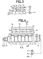
- each photosensitive detector D 12 , D 22 , D 32 ' is connected via a connection C 12 , C 22' C 32 ' ... to a device for injecting load DIC constituted by a diode D 'and by a grid Gp connected to a potential ⁇ P which controls the passage of the charges from the diode D' towards the input of a corresponding stage of the shift register R.
- the DIC is in fact constituted by a MOS transistor M '12, M' 22, M '32 whose drain is realized by the diode D', by the gate Gp and source induced by the stage input register A.
- a charge transfer shift register is used, each stage of which is constituted by a pair of electrodes connected to a control signal ⁇ 1 and by a pair of electrodes connected to a signal ⁇ 2 .
- Each pair of electrodes consists of a storage electrode and a transfer electrode.
- the asymmetry in the surface potentials necessary to make the transfer unilateral is carried out, for example, by an excess thickness of oxide or by an implantation of impurities of the same type as the substrate.
- Other types of shift registers with transfer of charge can be used.
- the shift register R comprises a charge injection device in series constituted by a diode De and gates G ' 1 and G' 2 .
- This charge injection device makes it possible to inject a charge Q o constituting a charge bottom, the role of which will be explained in detail below.
- the shift register R demultiplexes the charges integrated in the detectors of the photosensitive zone of the multilinear strip and transfers them sequentially to a charge-voltage reading stage of known type constituted for example by a grid G S and a diode D S connected to the source of a MOS transistor MR and to the input of an amplifier A giving the output signal S.
- the drain of the MOS transistor is connected to a constant voltage V R and its gate at a potential ⁇ R.
- the multilinear array according to the present invention further comprises an anti-dazzle device constituted by MOS transistors M 121 M 221 M 32 whose drain D B is brought to a polarization potential VDB, the gate G B is brought to a fixed voltage V B and the source consists of the diode D 'of injecting the charges from the detectors.
- an anti-dazzle device constituted by MOS transistors M 121 M 221 M 32 whose drain D B is brought to a polarization potential VDB, the gate G B is brought to a fixed voltage V B and the source consists of the diode D 'of injecting the charges from the detectors.
- the multilinear strip of the present invention is produced on a silicon substrate of type P.
- equivalent semiconductor substrates such as gallium arsenide or type N silicon substrates can also be used.
- the demultiplexing and reading system constituted by the charge injection device, the anti-dazzle device and the register R is produced on an N-type diffusion so as to effect a volume transfer at this level which improves the quality transfer and reduces noise.
- this zone can also be produced directly on the P-type substrate.
- the anti-dazzle device intended to avoid the distribution of excess charge from a backlit detector to neighboring detectors or to the demultiplexing and reading also avoids the introduction into the shift register of a quantity of charge exceeding the capacity of each of its stages.
- This latter function can also be performed using an anti-dazzle MOS transistor directly associated with each stage of the shift register. Examples of configuration of this MOS transistor associated with each stage of the register are shown in Figures 6a, 6b, 7a, 7b and 8a, 8b.
- the anti-dazzle MOS transistor is produced by the diode D ' B brought to a bias potential V'DB, the gate G' B brought to a fixed voltage V ' B and by the input stage of the register R, these various elements being produced in the zone N.
- the signal charge Q S transferred is too large compared to the capacity of each stage of the register R, the excess charges are discharged over the potential barrier formed under the grid G ' B.
- the area N extends only under part of the stages of the CCD register and the anti-glare MOS transistor is formed by the diode D'g produced by an N + type diffusion in the substrate P and brought to a bias potential V ′ DB , by the gate part of the register R covering the substrate P and by the gate part of the register R covering the area N.
- the excess charges are discharged over the potential barrier formed under the gate part of the register R covering the substrate P and due to the doping difference between the area N and the substrate P.
- FIGS. 8a and 8b an alternative embodiment of FIGS. 7a and 7b has been shown in which the diode D'g is not brought to a polarization potential V ' DB but polarized by the control potential ⁇ 1 of the register shifted.
- Figures 9 and 10 show another embodiment of the demultiplexing and reading system.
- the charges integrated by the photosensitive detectors are read directly in voltage and multiplexed using a register with logical shift R '.
- the conversion system shown comprises voltage reading means constituted by MOS transistors T 11 , T 12 ... T np .. T NP mounted in the follower stage.
- the gate G 1 of each MOS transistor T np is connected by a connection C 11 , C 12 ' ... C np , to a photosensitive detector D 11 , D 12 , ... D np ... produced by a diffusion of type N.
- the drain of the MOS transistors T np produced by the type N diffusion referenced N 2 + in FIG. 10a is connected to a bias voltage V DD .
- the source of the MOS transistors T n p referenced N 3 + in FIG. 10a is connected via a MOS transistor T playing the role of switch to a load TC.
- a single load is used for all the follower stages, which makes it possible to limit the power.
- the load TC is constituted by a depletion MOS transistor, the gate G 3 of which is connected to the source produced by the N-type diffusion referenced N 5 + in FIG. 10a, this source being polarized by a DC voltage V SS .
- charging could be carried out by other types of current sources or by a resistor.
- each gate G 2 of the MOS switch transistors T ' np is connected to one of the outputs of a logic shift register R' with serial input and parallel outputs.
- This shift register R ′ makes it possible to address and turn on one of the MOS transistors T ′ np, the other transistors being blocked.
- the following follower stages are multiplexed.
- an anti-dazzle device can be provided at each detector.
- This anti-dazzle device is constituted in the embodiment of FIG. 9 by a MOS transistor T " 11 , T" 12 whose drain is connected to a bias potential V DB , the gate to potential V GB and the source to the corresponding connection C 11 , C 12 , ...
- FIG. 10b represents the surface potentials in the substrate during the reading of a detector D n p.
- the charges created in the detector D n p by the radiation are stored in the capacity of the junction formed by this diffusion with the substrate.
- the charges stored in one of said capacitors are read when the corresponding output np of the shift register R 'is at logic level 1 so that the gate of the MOS transistor T' np receives a high voltage making said transistor pass, all the gates other MOS transistors playing the role of switch receiving a logic level "O" blocking said transistors.
- the MOS transistor T ' np behaves like a resistor, the transistor TC, namely the load, is connected to the follower transistor T and therefore a conventional follower stage is obtained, the bias voltage V DD being chosen to be much higher. at the bias voltage V SS as shown in Figure 10b.
- the detector D np being connected to the gate G 1 of the MOS transistor T np, a potential representative of the amount of charge integrated in the detector D n p is obtained at this gate. Indeed, as the detector D np is connected to the grid G I , the potential under this grid is aligned, taking into account the potential difference due to the insulator, on the potential at the level of the detector.
- the transistor T ' np is equivalent to a resistance
- the potential at the level of the diffusion N 4 + is aligned on the potential at the level of the diffusion N 3 + .
- the potential at the N 3 + diffusion is a function of the potential under the grid G 1 , because in a follower stage the potential difference is a constant.
- a voltage representative of the charges stored in the detector D np is therefore obtained at the level of the diffusion N 4 + . This voltage is sent through amplifier A to the output terminal S of the multilinear strip.
- the logic level "1" of the shift register R ' is shifted by one stage under the action of the clock H and then the input np is read. + 1. If the register R 'is a serial register, a logic level "1" is entered in the register at the start of each integration cycle. However, a looped logical shift register could be used.
- FIG. 11 shows a third embodiment of the demultiplexing and reading system.
- the charges integrated by the photosensitive detectors D 11 , D 12 , ... D np are read by the current flowing through the resistor R c located at the output.
- the demultiplexing and reading system shown comprises MOS transistors I ll , I 12 , ... I np , ... mounted as switches, the drains of which are connected to a DC voltage V DD by means of a resistor load R C.
- the sources of the MOS transistors I 11 , I 12 , ... I np , ... are connected via connections C 11 , C 12 , ... C np , ... to the detectors D 11 , D 12 , ... D np , ...
- These detectors are also connected, as in the embodiment of FIG. 9, to transistors T " 11 ' T" 12' ... T " np , ... d ' anti-glare.
- the gates of the MOS transistors I 11 , I 12 , ... I np , ... are connected to the outputs of a logic shift register R 'with serial input and parallel outputs identical to the register R' of the embodiment of FIG. 9.
- the charges created in the detector D np by the radiation are stored in the capacity formed by the junction D np with the substrate.
- the charges stored in this capacitor are read when the corresponding switching transistor I np is on, namely when a logic level "1" is applied to its gate. This reading is obtained by the output reproduction at using the amplifier A of the voltage produced by the current of the charges stored through the resistor RC connected to the direct voltage V DD .
- the voltage on the detector D takes a value defined by the DC voltage V DD .
- the detector is then isolated by the opening of the switch transistor I np , by sending a logic level "O" to its gate.
- FIGS. 1 to 11 various embodiments of a multilinear strip with elementary charge transfer have been shown in which the detectors are read individually.
- the detectors are read individually.
- an individual reading of the detectors is carried out, the processing of the signals obtained, in particular the TDI function, being carried out outside the device. Therefore, it is possible to modify the structure of the elementary bar or to carry out a scanning which is not perpendicular to the lines of the photosensitive zone, so as to associate during the treatment, detectors located on different elementary bars which reduces or even cancels image connection faults.
- the various elementary bars M-1, M and M + 1 are produced by multilinear bars of the type described with reference to FIG. 2.
- the different lines of the photosensitive zone are aligned with each other but to avoid connection faults at the ends of each strip, the scanning takes place obliquely in direction B. Therefore, at the processing of the detectors provided at the ends, the detector referenced A 'on the last line of the strip M-1 is associated with the detector referenced A on the first line of the strip M.
- each line of detectors is offset by a detector relative to the adjacent lines. Therefore, the alignment of the missing detectors is carried out according to the oblique arrow F in dashed lines. In this case, the scanning B is carried out perpendicular to the photosensitive lines. Thus, at the ends of each strip, the detector referenced A of strip M-1 is treated with the detector referenced A 'of strip M. It is obvious to those skilled in the art that each line of detector can also be offset by several detectors from adjacent lines.
- each line of detectors of an elementary strip is offset by half a detector with respect to the adjacent lines.
- the direction of the missing detectors namely the edge of the strip
- the scanning direction B is oblique, the detector referenced A on the strip M-1 being treated with the detector referenced A 'on the bar M.
- each line of detectors can also be offset by a part of the detector with respect to the adjacent lines.
- FIG. 15 can be adopted. As shown in this figure, locally or at the two lateral ends of an elementary bar, one or two additional lines of N detectors are added, N corresponding to the number of lines in the bar.
- the delays and the above sum can be obtained by analog or digital means according to the principle represented in FIG. 16.
- the elements of the different lines to be composed are symbolized by contactors d, c, b, a.
- the signal of the element d after having passed into a register Re delaying it by T is sent to an adder ⁇ which receives on its other input the signal of the element c.
- the output c + d after having passed to a register Re giving it a delay T is sent to an adder ⁇ whose other input receives the signal from the element b.
- the sum b + c + d after being delayed by a time T is sent to an adder ⁇ whose other input receives the signal from element a and the output S gives the compound signal.
- the output of an elementary bar can be connected to the next bar by a switch so as to compose elements located on different bars.
- FIG. 16 represents only one principle of realization of the TDI function.
- the charge transfer shift registers can be positioned on each side of the photosensitive zone or else laterally or even possibly folded back on themselves.
Landscapes
- Solid State Image Pick-Up Elements (AREA)
- Transforming Light Signals Into Electric Signals (AREA)
Applications Claiming Priority (2)
| Application Number | Priority Date | Filing Date | Title |
|---|---|---|---|
| FR8402573 | 1984-02-21 | ||
| FR8402573A FR2559957B1 (fr) | 1984-02-21 | 1984-02-21 | Barrette multilineaire a transfert de charge |
Publications (2)
| Publication Number | Publication Date |
|---|---|
| EP0153251A1 true EP0153251A1 (de) | 1985-08-28 |
| EP0153251B1 EP0153251B1 (de) | 1989-03-29 |
Family
ID=9301208
Family Applications (1)
| Application Number | Title | Priority Date | Filing Date |
|---|---|---|---|
| EP85400279A Expired EP0153251B1 (de) | 1984-02-21 | 1985-02-15 | Bildaufnahmevorrichtung mit stabförmiger multilinearer Ladungsverschiebungsanordnung |
Country Status (7)
| Country | Link |
|---|---|
| US (1) | US4744057A (de) |
| EP (1) | EP0153251B1 (de) |
| JP (1) | JP2572743B2 (de) |
| DE (1) | DE3569173D1 (de) |
| FR (1) | FR2559957B1 (de) |
| HK (1) | HK42891A (de) |
| SG (1) | SG97290G (de) |
Cited By (2)
| Publication number | Priority date | Publication date | Assignee | Title |
|---|---|---|---|---|
| FR2598250A1 (fr) * | 1986-04-30 | 1987-11-06 | Thomson Csf | Panneau de prise de vue radiologique, et procede de fabrication |
| EP1865714A4 (de) * | 2005-03-30 | 2010-12-15 | Sony Corp | Ansteuerverfahren zur ansteuerung eines elements mit kapazitiver impedanz, ansteuereinrichtung und bildgebungseinrichtung |
Families Citing this family (18)
| Publication number | Priority date | Publication date | Assignee | Title |
|---|---|---|---|---|
| US4980771A (en) * | 1988-02-18 | 1990-12-25 | Victor Company Of Japan, Ltd. | Imaging device and imaging apparatus including the imaging device |
| FR2638042A1 (fr) * | 1988-10-14 | 1990-04-20 | Thomson Csf | Procede pour reduire la remanence d'un phototransistor, notamment de type nipin |
| FR2653626A1 (fr) * | 1989-10-24 | 1991-04-26 | Thomson Composants Militaires | Capteur photosensible a temps d'integration programmable. |
| US5237190A (en) * | 1992-07-31 | 1993-08-17 | Hualon Microelectronics Corporation | Charge-coupled-device color image sensor |
| JPH06204450A (ja) * | 1992-12-28 | 1994-07-22 | Toshiba Corp | 固体撮像装置 |
| US5324968A (en) * | 1993-11-18 | 1994-06-28 | Eastman Kodak Company | CCD image sensor |
| WO1995020825A1 (en) * | 1994-01-31 | 1995-08-03 | Scientific Imaging Technologies, Inc. | Charge-coupled device array for spectroscopic detection |
| US5432335A (en) * | 1994-03-14 | 1995-07-11 | Princeton Instruments, Inc. | Charge-coupled device for spectroscopic detection |
| GB2289983B (en) | 1994-06-01 | 1996-10-16 | Simage Oy | Imaging devices,systems and methods |
| JP2907058B2 (ja) * | 1995-04-21 | 1999-06-21 | 富士ゼロックス株式会社 | 蓄積手段を持つイメージセンサ及び画像読取装置 |
| FR2743462B1 (fr) * | 1996-01-04 | 1998-01-30 | Commissariat Energie Atomique | Dispositif de lecture de barrettes de detecteurs avec effet tdi |
| US5693968A (en) * | 1996-07-10 | 1997-12-02 | Board Of Supervisors Of Louisiana State University And Agricultural And Mechanical College | Bi-directional, fast-timing, charge coupled device |
| US9029793B2 (en) * | 1998-11-05 | 2015-05-12 | Siemens Aktiengesellschaft | Imaging device |
| GB0224689D0 (en) | 2002-10-23 | 2002-12-04 | Simage Oy | Formation of contacts on semiconductor substrates |
| EP1554760B1 (de) * | 2002-10-25 | 2009-08-19 | Ipl Intellectual Property Licensing Limited | Schaltungssubstrat und verfahren |
| US7196304B2 (en) * | 2004-01-29 | 2007-03-27 | Micron Technology, Inc. | Row driver for selectively supplying operating power to imager pixel |
| US20110073982A1 (en) * | 2007-05-25 | 2011-03-31 | Armstrong J Joseph | Inspection system using back side illuminated linear sensor |
| US10903258B2 (en) * | 2017-10-11 | 2021-01-26 | Kla Corporation | Image sensors with grounded or otherwise biased channel-stop contacts |
Citations (2)
| Publication number | Priority date | Publication date | Assignee | Title |
|---|---|---|---|---|
| EP0038725A1 (de) * | 1980-04-23 | 1981-10-28 | Thomson-Csf | Photoempfindliche Vorrichtung, die durch Ladungsübertragung abgelesen wird, sowie eine Fernsehkamera, die eine solche Vorrichtung enthält |
| US4349743A (en) * | 1979-11-14 | 1982-09-14 | Hitachi, Ltd. | Solid-state imaging device |
Family Cites Families (6)
| Publication number | Priority date | Publication date | Assignee | Title |
|---|---|---|---|---|
| CA948331A (en) * | 1971-03-16 | 1974-05-28 | Michael F. Tompsett | Charge transfer imaging devices |
| US3953837A (en) * | 1974-11-27 | 1976-04-27 | Texas Instruments Incorporated | Dual serial-parallel-serial analog memory |
| US4306160A (en) * | 1979-07-25 | 1981-12-15 | Hughes Aircraft Company | Charge coupled device staircase electrode multiplexer |
| JPS5683980A (en) * | 1979-12-13 | 1981-07-08 | Fujitsu Ltd | Electric charge transfer device |
| JPS56109076A (en) * | 1980-01-31 | 1981-08-29 | Fujitsu Ltd | Solid-state image sensor |
| US4513313A (en) * | 1982-12-07 | 1985-04-23 | Canon Kabushiki Kaisha | Solid state imaging device |
-
1984
- 1984-02-21 FR FR8402573A patent/FR2559957B1/fr not_active Expired
-
1985
- 1985-02-15 US US06/701,948 patent/US4744057A/en not_active Expired - Lifetime
- 1985-02-15 DE DE8585400279T patent/DE3569173D1/de not_active Expired
- 1985-02-15 EP EP85400279A patent/EP0153251B1/de not_active Expired
- 1985-02-21 JP JP60031697A patent/JP2572743B2/ja not_active Expired - Lifetime
-
1990
- 1990-11-30 SG SG972/90A patent/SG97290G/en unknown
-
1991
- 1991-05-30 HK HK428/91A patent/HK42891A/xx not_active IP Right Cessation
Patent Citations (2)
| Publication number | Priority date | Publication date | Assignee | Title |
|---|---|---|---|---|
| US4349743A (en) * | 1979-11-14 | 1982-09-14 | Hitachi, Ltd. | Solid-state imaging device |
| EP0038725A1 (de) * | 1980-04-23 | 1981-10-28 | Thomson-Csf | Photoempfindliche Vorrichtung, die durch Ladungsübertragung abgelesen wird, sowie eine Fernsehkamera, die eine solche Vorrichtung enthält |
Non-Patent Citations (1)
| Title |
|---|
| IEEE TRANSACTIONS ON ELECTRON DEVICES, vol. ED-27, no. 1, janvier 1980, pages 175-188, IEEE, New York, US; P. FELIX et al.: "CCD readout of infrared hybrid focal-plane arrays" * |
Cited By (4)
| Publication number | Priority date | Publication date | Assignee | Title |
|---|---|---|---|---|
| FR2598250A1 (fr) * | 1986-04-30 | 1987-11-06 | Thomson Csf | Panneau de prise de vue radiologique, et procede de fabrication |
| EP0245147A1 (de) * | 1986-04-30 | 1987-11-11 | Thomson-Csf | Röntgen-Bilderfassungstafel und deren Herstellungsverfahren |
| US4810881A (en) * | 1986-04-30 | 1989-03-07 | Thomson-Csf | Panel for X-ray photography and method of manufacture |
| EP1865714A4 (de) * | 2005-03-30 | 2010-12-15 | Sony Corp | Ansteuerverfahren zur ansteuerung eines elements mit kapazitiver impedanz, ansteuereinrichtung und bildgebungseinrichtung |
Also Published As
| Publication number | Publication date |
|---|---|
| JP2572743B2 (ja) | 1997-01-16 |
| JPS60202964A (ja) | 1985-10-14 |
| EP0153251B1 (de) | 1989-03-29 |
| US4744057A (en) | 1988-05-10 |
| HK42891A (en) | 1991-06-07 |
| SG97290G (en) | 1991-04-05 |
| FR2559957A1 (fr) | 1985-08-23 |
| FR2559957B1 (fr) | 1986-05-30 |
| DE3569173D1 (en) | 1989-05-03 |
Similar Documents
| Publication | Publication Date | Title |
|---|---|---|
| EP0153251B1 (de) | Bildaufnahmevorrichtung mit stabförmiger multilinearer Ladungsverschiebungsanordnung | |
| EP0168267B1 (de) | Aus mehreren Zeilen bestehende ladungsgekoppelte Sensoranordnung und Abtastverfahren | |
| EP0038725B1 (de) | Photoempfindliche Vorrichtung, die durch Ladungsübertragung abgelesen wird, sowie eine Fernsehkamera, die eine solche Vorrichtung enthält | |
| EP0367650B1 (de) | Photoempfindliche Vorrichtung mit Signalverstärkung im Bereich der photoempfindlichen Punkte | |
| EP0145543B1 (de) | Ladungsgekoppelte mehrzeilige lineare Anordnung | |
| EP0435773B1 (de) | Bildaufnahmeeinrichtung mit integrierten Ablenkschaltungen | |
| FR2704095A1 (fr) | Capteur d'images du type dispositif à couplage de charge. | |
| EP1416538A2 (de) | Photodetektor für einen Bildsensor | |
| FR2549328A1 (fr) | Dispositif photosensible a l'etat solide | |
| FR2846147A1 (fr) | Commande d'une cellule photosensible | |
| EP0276594A1 (de) | Überlaufvorrichtung für einen Ladungsübertragungs-Bildsensor und eine solche Vorrichtung enthaltender Bildsensor | |
| EP0149948B1 (de) | Photoempfindliche Festkörperanordnungen | |
| WO2004105136A1 (fr) | Capteur d'image matriciel en technologie cmos | |
| EP0737002A1 (de) | CCD-Ausleseregister mit mehreren Ausgängen | |
| EP3829160B1 (de) | Pixel mit einstellbarem dynamikbereich zur geräuschreduzierung | |
| EP0130529B1 (de) | Netz von adressierbaren Fotodetektoren | |
| FR2759509A1 (fr) | Circuit integrateur a linearite amelioree | |
| EP4075506A1 (de) | Pixel-matrix mit analoger summierung und global shutter | |
| FR2460079A1 (fr) | Mosaique de detecteurs de rayonnement lue par un dispositif semi-conducteur, et systeme de prise de vues comportant une telle mosaique | |
| EP0129470A1 (de) | Festkörper photoempfindliche Anordnung | |
| FR2635936A1 (fr) | Element et reseau de detection de lumiere | |
| EP0275740B1 (de) | Ausleseschaltung für eine lichtempfindliche Zeilenübertragungsanordnung, lichtempfindliche Zeilenübertragungsanordnung mit einer solchen Schaltung und Ausleseverfahren einer solchen Anordnung | |
| FR2682813A1 (fr) | Dispositif de visualisation de rayonnements infra-rouges. | |
| FR2682814A1 (fr) | Dispositif de visualisation de rayonnements infra-rouges. | |
| FR2672759A1 (fr) | Capteur d'images a semiconducteurs, a stockage de charge. |
Legal Events
| Date | Code | Title | Description |
|---|---|---|---|
| PUAI | Public reference made under article 153(3) epc to a published international application that has entered the european phase |
Free format text: ORIGINAL CODE: 0009012 |
|
| AK | Designated contracting states |
Designated state(s): DE GB NL |
|
| 17P | Request for examination filed |
Effective date: 19850912 |
|
| 17Q | First examination report despatched |
Effective date: 19861125 |
|
| GRAA | (expected) grant |
Free format text: ORIGINAL CODE: 0009210 |
|
| AK | Designated contracting states |
Kind code of ref document: B1 Designated state(s): DE GB NL |
|
| REF | Corresponds to: |
Ref document number: 3569173 Country of ref document: DE Date of ref document: 19890503 |
|
| RAP4 | Party data changed (patent owner data changed or rights of a patent transferred) |
Owner name: THOMSON-CSF |
|
| GBT | Gb: translation of ep patent filed (gb section 77(6)(a)/1977) | ||
| PLBE | No opposition filed within time limit |
Free format text: ORIGINAL CODE: 0009261 |
|
| STAA | Information on the status of an ep patent application or granted ep patent |
Free format text: STATUS: NO OPPOSITION FILED WITHIN TIME LIMIT |
|
| 26N | No opposition filed | ||
| REG | Reference to a national code |
Ref country code: GB Ref legal event code: IF02 |
|
| PGFP | Annual fee paid to national office [announced via postgrant information from national office to epo] |
Ref country code: NL Payment date: 20040205 Year of fee payment: 20 |
|
| PGFP | Annual fee paid to national office [announced via postgrant information from national office to epo] |
Ref country code: GB Payment date: 20040211 Year of fee payment: 20 |
|
| PGFP | Annual fee paid to national office [announced via postgrant information from national office to epo] |
Ref country code: DE Payment date: 20040226 Year of fee payment: 20 |
|
| PG25 | Lapsed in a contracting state [announced via postgrant information from national office to epo] |
Ref country code: GB Free format text: LAPSE BECAUSE OF EXPIRATION OF PROTECTION Effective date: 20050214 |
|
| PG25 | Lapsed in a contracting state [announced via postgrant information from national office to epo] |
Ref country code: NL Free format text: LAPSE BECAUSE OF EXPIRATION OF PROTECTION Effective date: 20050215 |
|
| REG | Reference to a national code |
Ref country code: GB Ref legal event code: PE20 |
|
| NLV7 | Nl: ceased due to reaching the maximum lifetime of a patent |
Effective date: 20050215 |