EP0155178B1 - Überzugsfilm, Verfahren und Vorrichtung zur Herstellung dieses Filmes - Google Patents
Überzugsfilm, Verfahren und Vorrichtung zur Herstellung dieses Filmes Download PDFInfo
- Publication number
- EP0155178B1 EP0155178B1 EP85301709A EP85301709A EP0155178B1 EP 0155178 B1 EP0155178 B1 EP 0155178B1 EP 85301709 A EP85301709 A EP 85301709A EP 85301709 A EP85301709 A EP 85301709A EP 0155178 B1 EP0155178 B1 EP 0155178B1
- Authority
- EP
- European Patent Office
- Prior art keywords
- substrate
- anode
- electrode
- coating film
- target
- Prior art date
- Legal status (The legal status is an assumption and is not a legal conclusion. Google has not performed a legal analysis and makes no representation as to the accuracy of the status listed.)
- Expired - Lifetime
Links
- 238000000576 coating method Methods 0.000 title claims description 48
- 239000011248 coating agent Substances 0.000 title claims description 45
- 238000000034 method Methods 0.000 title claims description 16
- 239000000758 substrate Substances 0.000 claims description 37
- 238000004544 sputter deposition Methods 0.000 claims description 30
- 239000007789 gas Substances 0.000 claims description 27
- 229910003481 amorphous carbon Inorganic materials 0.000 claims description 15
- UFHFLCQGNIYNRP-UHFFFAOYSA-N Hydrogen Chemical compound [H][H] UFHFLCQGNIYNRP-UHFFFAOYSA-N 0.000 claims description 13
- 239000001257 hydrogen Substances 0.000 claims description 11
- 229910052739 hydrogen Inorganic materials 0.000 claims description 11
- OKTJSMMVPCPJKN-UHFFFAOYSA-N Carbon Chemical compound [C] OKTJSMMVPCPJKN-UHFFFAOYSA-N 0.000 claims description 9
- YCKRFDGAMUMZLT-UHFFFAOYSA-N Fluorine atom Chemical compound [F] YCKRFDGAMUMZLT-UHFFFAOYSA-N 0.000 claims description 8
- 239000011737 fluorine Substances 0.000 claims description 8
- 229910052731 fluorine Inorganic materials 0.000 claims description 8
- 239000004065 semiconductor Substances 0.000 claims description 7
- 229910002804 graphite Inorganic materials 0.000 claims description 6
- 239000010439 graphite Substances 0.000 claims description 6
- 229910052799 carbon Inorganic materials 0.000 claims description 3
- IJGRMHOSHXDMSA-UHFFFAOYSA-N Atomic nitrogen Chemical compound N#N IJGRMHOSHXDMSA-UHFFFAOYSA-N 0.000 claims 2
- ZOXJGFHDIHLPTG-UHFFFAOYSA-N Boron Chemical compound [B] ZOXJGFHDIHLPTG-UHFFFAOYSA-N 0.000 claims 2
- 229910052796 boron Inorganic materials 0.000 claims 2
- BHEPBYXIRTUNPN-UHFFFAOYSA-N hydridophosphorus(.) (triplet) Chemical compound [PH] BHEPBYXIRTUNPN-UHFFFAOYSA-N 0.000 claims 2
- 229910052757 nitrogen Inorganic materials 0.000 claims 1
- 239000010408 film Substances 0.000 description 44
- 239000000463 material Substances 0.000 description 18
- 235000019589 hardness Nutrition 0.000 description 11
- 238000000151 deposition Methods 0.000 description 8
- 230000008021 deposition Effects 0.000 description 8
- 230000000694 effects Effects 0.000 description 7
- 239000002184 metal Substances 0.000 description 7
- 229910052751 metal Inorganic materials 0.000 description 7
- XKRFYHLGVUSROY-UHFFFAOYSA-N Argon Chemical compound [Ar] XKRFYHLGVUSROY-UHFFFAOYSA-N 0.000 description 5
- 238000005299 abrasion Methods 0.000 description 5
- 230000003247 decreasing effect Effects 0.000 description 5
- 230000015572 biosynthetic process Effects 0.000 description 4
- 230000007547 defect Effects 0.000 description 4
- 230000003287 optical effect Effects 0.000 description 4
- 239000002245 particle Substances 0.000 description 4
- 239000010409 thin film Substances 0.000 description 4
- 229910052786 argon Inorganic materials 0.000 description 3
- 238000007796 conventional method Methods 0.000 description 3
- 238000010586 diagram Methods 0.000 description 3
- 238000004519 manufacturing process Methods 0.000 description 3
- 230000003647 oxidation Effects 0.000 description 3
- 238000007254 oxidation reaction Methods 0.000 description 3
- 239000004033 plastic Substances 0.000 description 3
- 229920003023 plastic Polymers 0.000 description 3
- 229910001218 Gallium arsenide Inorganic materials 0.000 description 2
- 229910000661 Mercury cadmium telluride Inorganic materials 0.000 description 2
- XUIMIQQOPSSXEZ-UHFFFAOYSA-N Silicon Chemical compound [Si] XUIMIQQOPSSXEZ-UHFFFAOYSA-N 0.000 description 2
- QVGXLLKOCUKJST-UHFFFAOYSA-N atomic oxygen Chemical compound [O] QVGXLLKOCUKJST-UHFFFAOYSA-N 0.000 description 2
- 239000000498 cooling water Substances 0.000 description 2
- 238000005520 cutting process Methods 0.000 description 2
- 238000009501 film coating Methods 0.000 description 2
- 238000011835 investigation Methods 0.000 description 2
- 239000002932 luster Substances 0.000 description 2
- 150000002739 metals Chemical class 0.000 description 2
- 239000001301 oxygen Substances 0.000 description 2
- 229910052760 oxygen Inorganic materials 0.000 description 2
- 238000007789 sealing Methods 0.000 description 2
- 229910052710 silicon Inorganic materials 0.000 description 2
- 239000010703 silicon Substances 0.000 description 2
- 239000000126 substance Substances 0.000 description 2
- 238000003466 welding Methods 0.000 description 2
- 229910052582 BN Inorganic materials 0.000 description 1
- PZNSFCLAULLKQX-UHFFFAOYSA-N Boron nitride Chemical compound N#B PZNSFCLAULLKQX-UHFFFAOYSA-N 0.000 description 1
- 239000004215 Carbon black (E152) Substances 0.000 description 1
- 229910045601 alloy Inorganic materials 0.000 description 1
- 239000000956 alloy Substances 0.000 description 1
- 229910021417 amorphous silicon Inorganic materials 0.000 description 1
- 230000003064 anti-oxidating effect Effects 0.000 description 1
- -1 argon ion Chemical class 0.000 description 1
- 230000005540 biological transmission Effects 0.000 description 1
- 239000003990 capacitor Substances 0.000 description 1
- 125000004432 carbon atom Chemical group C* 0.000 description 1
- 239000011203 carbon fibre reinforced carbon Substances 0.000 description 1
- 230000006866 deterioration Effects 0.000 description 1
- 229910003460 diamond Inorganic materials 0.000 description 1
- 239000010432 diamond Substances 0.000 description 1
- 230000005684 electric field Effects 0.000 description 1
- 238000004070 electrodeposition Methods 0.000 description 1
- 238000010894 electron beam technology Methods 0.000 description 1
- 230000007613 environmental effect Effects 0.000 description 1
- 229930195733 hydrocarbon Natural products 0.000 description 1
- 239000011810 insulating material Substances 0.000 description 1
- 239000012212 insulator Substances 0.000 description 1
- 230000003449 preventive effect Effects 0.000 description 1
- 239000011253 protective coating Substances 0.000 description 1
- 230000005855 radiation Effects 0.000 description 1
- HBMJWWWQQXIZIP-UHFFFAOYSA-N silicon carbide Chemical compound [Si+]#[C-] HBMJWWWQQXIZIP-UHFFFAOYSA-N 0.000 description 1
- 229910010271 silicon carbide Inorganic materials 0.000 description 1
- 239000013077 target material Substances 0.000 description 1
- TXEYQDLBPFQVAA-UHFFFAOYSA-N tetrafluoromethane Chemical compound FC(F)(F)F TXEYQDLBPFQVAA-UHFFFAOYSA-N 0.000 description 1
Images

Classifications
-
- H—ELECTRICITY
- H01—ELECTRIC ELEMENTS
- H01J—ELECTRIC DISCHARGE TUBES OR DISCHARGE LAMPS
- H01J37/00—Discharge tubes with provision for introducing objects or material to be exposed to the discharge, e.g. for the purpose of examination or processing thereof
- H01J37/32—Gas-filled discharge tubes
- H01J37/34—Gas-filled discharge tubes operating with cathodic sputtering
- H01J37/3402—Gas-filled discharge tubes operating with cathodic sputtering using supplementary magnetic fields
-
- C—CHEMISTRY; METALLURGY
- C23—COATING METALLIC MATERIAL; COATING MATERIAL WITH METALLIC MATERIAL; CHEMICAL SURFACE TREATMENT; DIFFUSION TREATMENT OF METALLIC MATERIAL; COATING BY VACUUM EVAPORATION, BY SPUTTERING, BY ION IMPLANTATION OR BY CHEMICAL VAPOUR DEPOSITION, IN GENERAL; INHIBITING CORROSION OF METALLIC MATERIAL OR INCRUSTATION IN GENERAL
- C23C—COATING METALLIC MATERIAL; COATING MATERIAL WITH METALLIC MATERIAL; SURFACE TREATMENT OF METALLIC MATERIAL BY DIFFUSION INTO THE SURFACE, BY CHEMICAL CONVERSION OR SUBSTITUTION; COATING BY VACUUM EVAPORATION, BY SPUTTERING, BY ION IMPLANTATION OR BY CHEMICAL VAPOUR DEPOSITION, IN GENERAL
- C23C14/00—Coating by vacuum evaporation, by sputtering or by ion implantation of the coating forming material
- C23C14/06—Coating by vacuum evaporation, by sputtering or by ion implantation of the coating forming material characterised by the coating material
- C23C14/0605—Carbon
-
- Y—GENERAL TAGGING OF NEW TECHNOLOGICAL DEVELOPMENTS; GENERAL TAGGING OF CROSS-SECTIONAL TECHNOLOGIES SPANNING OVER SEVERAL SECTIONS OF THE IPC; TECHNICAL SUBJECTS COVERED BY FORMER USPC CROSS-REFERENCE ART COLLECTIONS [XRACs] AND DIGESTS
- Y10—TECHNICAL SUBJECTS COVERED BY FORMER USPC
- Y10T—TECHNICAL SUBJECTS COVERED BY FORMER US CLASSIFICATION
- Y10T428/00—Stock material or miscellaneous articles
- Y10T428/30—Self-sustaining carbon mass or layer with impregnant or other layer
Definitions
- the present invention relates to a coating film of amorphous carbon and a method and apparatus for producing the same.
- a coating film of amorphous carbon generally has a high hardness, high oxidation resistance, high thermal resistance, high electrical resistance and high thermal conductivity.
- plastics materials and common metals are susceptible to surface scratch so that their surfaces, while initially having excellent luster, gradually lose their luster which damages their appearance. This has been considered to be due to the fact that these plastics material and metals are relatively soft and have low abrasion resistance.
- the cell In the case of a solar cell comprising amorphous silicon, etc., which contains a large amount of hydrogen or a large amount of hydrogen and fluorine, the cell essentially has a low energy converting efficiency and this is compensated for by means of an increased surface area or the like.
- a need for the development of materials of higher efficiencies for the surface coating films in view of the necessity to ensure a sufficient amount of incident light to the solar cell.
- the conventional silicon semiconductors are subject to the limitation that the forbidden band gap may be as narrow as 1.21 eV and they cannot be used at high temperatures, thus giving rise to a need for the development of a material having wider range of working temperatures.
- the conventional sputtering methods include one in which an argon plasma is produced by applying a voltage across an anode and a cathode in argon gas at a pressure of about 0.133 to 1.33 Pa (10 ⁇ 3 to 10 ⁇ 2 Torr) and a target material is sputtered by the argon ion thereby forming an alloy coating on the substrate.
- a method of producing an amorphous carbon coating film on a substrate which comprises sputtering a carbonaceous e.g. graphite target electrode in a vacuum chamber characterised in that the current density between the target cathode and a corresponding anode is maintained at a value between 11.3 and 14.7 mA/cm2, the cathode and anode being arranged to create a plasma state region (A) between them, to which region the substrate is not directly exposed, and the substrate is maintained at between room temperature and 100°C, the chamber containing hydrogen and/or fluorine gas at a pressure of between 6.665 and 666.5 Pa (0.05 and 5.0 Torr), thereby producing an amorphous carbon coating film in which the value of H/C or (H + F)/C in terms of an atomic ratio is between 0.5 and 0.9, the current density being defined as the current through the anode per unit area of the target electrode.
- a carbonaceous e.g. graphite target electrode in a vacuum chamber character
- an amorphous carbon coating film on a substrate produced by sputtering a carbonaceous, eg graphite, target cathode characterised in that the current density between the target cathode and a corresponding anode is maintained at a value between 11.3 and 14.7 mA/cm2, the cathode and anode being arranged to create a plasma state region (A) between them, to which region the substrate is not directly exposed, and the substrate is maintained at between room temperature and 100°C, the chamber containing hydrogen and/or fluorine gas at a pressure of between 6.665 and 666.5 Pa (0.05 and 5.0 Torr), whereby in the carbon coating the value of H/C or (H+F)/C in terms of an atomic ratio is between 0.5 and 0.9, the current density being defined as the current through the anode per unit area of the target cathode.
- a carbonaceous, eg graphite, target cathode characterised in that the current density between the target cathode
- a sputtering apparatus for producing an amorphous carbon coating film on a substrate
- the apparatus comprising a vacuum chamber having an atmosphere gas inlet pipe, an exhaust pipe, an electron drawing anode, a carbonaceous, eg graphite, target electrode connected to a power source and positioned opposite to the anode, and means for producing a magnetic field to provide a directionality for a plasma, characterised by means for mounting a substrate on an inner wall of the vacuum chamber in a region (C) which during sputtering is not directly exposed to the plasma, and means for maintaining the substrate at between room temperature and 100°C, and being further characterised in that the power source is a high frequency source.
- a further electrode is arranged between the anode and the target electrode which, in use, is maintained at ground potential or is connected to another power source, the further electrode having a large number of holes for adjusting the amount of the plasma.
- the present invention has arisen from various studies and investigations made in view of the foregoing disadvantages of the conventional methods, in order to provide an amorphous carbon coating film having a high hardness, high oxidation resistance, high abrasion resistance, high thermal resistance, high thermal conductivity and high electric resistance properties. It has resulted in a production method and an apparatus capable of preventing for example various difficulties assumed to be due to the fact that a substrate is placed in a plasma and the production of a coating film of a material having excellent uniformity. This has led to the resulting discovery that an amorphous carbon coating film can be formed having excellent properties by effecting a sputtering operation including various specific parameters over and above a conventional sputtering method.
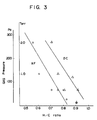
- the value of the H/C ratio can be reduced by effecting the sputtering operation with an increased gas pressure, that decreasing the H/C ratio of the coating material to 0.5 or less has the effect of reducing the hardness of the coating film thereby making it impractical, and that increasing the H/C ratio to exceed 0.9 is not desirable since the optical band gap or the electric resistance is decreased and hence the insulating capability is deteriorated.
- the H/C ratio of the coating film of material is in a range between 0.5 and 0.9.
- the gas pressure is in a range between 6.665 Pa and 666.5 Pa (0.5 to 5 Torr) during the sputtering.
- the range of working relative current densities should be selected to be 11.3 to 14.7 mA/cm2.
- a coating film of material produced in accordance with the present invention has a very high hardness, high thermal resistance and high electric resistance, is high in infrared ray transparency and is excellent in chemical resistance, moisture resistance and scratch resistance. More specifically, the coating may enjoy the following effects.
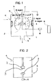
- numeral 1 designates a vacuum chamber, 4 an atmosphere gas inlet pipe, and 5 an exhaust pipe connected directly to a vacuum pump which is not shown to maintain a vacuum.
- Numeral 7 designates an electron drawing counter electrode at the ground potential, and 2 a carbonaceous electrode connected to a high frequency (RF) power source 6 through a matching box 8.
- RF radio frequency
- Numeral 3 designates deposition substrates arranged inside the container but outside the transport area of a plasma-excited source in contrast to conventional techniques. It is to be noted that hydrogen gas or any other gas is introduced through the atmosphere gas inlet pipe 4.
- the interior of the vacuum chamber is considered divided into three regions, i.e. A region, B region and C region as schematically shown in the Figure 1.
- the A region represents the area enclosed by curved lines a which is the plasma state environment produced between the electrodes and the vicinity around the electrodes; carbon and hydrocarbon radicals consisting two carbon atoms or less such as C, CH, CH2, CH3, CH4, C2H4 and C2H6 are generated from the target electrode 2 in this region.
- the B region represents the area enclosed by a curved line b outside the electrodes 2 and 7 and in this region the above-mentioned particles contained in the plasma are transported at a velocity which is determined by the pressure of the atmosphere gas and the voltage across the electrodes.
- the C region represents the area other than the A region and the B region and in this region the transported particles are softly deposited on the deposition substrates arranged on the container inner walls.
- charged particles (constituting the majority of the transported particles) are susceptible to the effects of an electric field or the like, therefore it is necessary to take this into consideration so that the C region is maintained at a uniform potential, e.g., around ground potential.
- the substrates are never directly exposed to the plasma produced between the target electrode and the counter electrode so that the deposition and bombardment by protons and electrons do not occur simultaneously at the substrate.
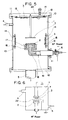
- the vacuum chamber 1 is composed of two covers and a cylinder having three flanges which are sealed with O-rings.
- Numeral 10 designates a metal upper cover sealed with an O-ring.
- Numeral 12 designates a lower cover sealed by a sealing method which allows it to perform the same function as the upper cover 10. It is constructed so that a hermetic sealing can be provided by means of welding or the like, ignoring a specially provided opening 5.
- Numeral 13 designates insulating terminals or supports, 14 electrically grounded receptors, 3 deposition substrates made of an insulating material or metal, and 15 substrate supporting members.
- the deposition substrates 3 are arranged in positions on the upper and side walls of the chamber which are external to the plasma generating section and the travel path of the plasma, they are not necessarily limited to these positions since it is only necessary that they are located outside the plasma excited source which is indicated as the C region in Fig. 1.
- Numeral 2 designates a carbonaceous target, 16 an electrode box, 17 a magnetron, 18 a cooling water supplying metal pipe, and 19 a drain pipe. The end of the cooling water pipe 18 outside the vacuum chamber is sealed watertight by welding.
- Numeral 20 designates a thermocouple.
- Numeral 7 designates a counter electrode for the target 2 and the target electrode 2 includes a connector which is provided outside the vacuum chamber 1 for connection with a high frequency power source.
- the matching box and the high frequency power source 6 shown in Fig. 1 are connected to the connector, although they are not shown.
- Numeral 4 designates an atmosphere gas inlet pipe connected to the vacuum chamber 1 so as to introduce an atmosphere gas consisting of hydrogen or hydrogen and fluorine.
- An exhaust pipe 5 is arranged to reduce the internal pressure of the vacuum chamber 1 through a vacuum pump which is not shown.
- the following table shows the results of a sputtering operating effected for 2 hours by applying a high frequency power of 13.56 MHz and using high-purity hydrogen of 99.999 vol. % as the atmosphere gas in a sputtering apparatus employing the above-mentioned deposition substrate arrangement and a sputtering apparatus having the substrate arranged in the counter electrode position for purposes of comparison.
- the sputtering conditions were as follows.
- the mesh electrode may literally be in the form of a mesh, it may also be a metal sheet formed with an innumerable number of pin holes so as to obtain the same effect as the mesh. Also, since the essential point is the adjustment of the amount of plasma, the invention is not limited to the method employing a grounded mesh and the same object can be accomplished by for example applying the potential supplied from a separate power supply to the plasma adjusting electrode.
- the amount of plasma may be adjusted by for example sliding the mesh to change its position as shown by the arrows in Fig. 6.
- Example 1 was repeated except that a fluorine gas or a mixed gas of hydrogen and fluorine was used in place of the hydrogen gas.
- the thermal resistance (the temperature at which the optical gap starts decreasing) attained by the amorphous carbon film was improved by the use of the mixed gas to from 300°C to 500°C.
- the use of carbon fluoride for the target improved the thermal resistance to 500°C.
Landscapes
- Chemical & Material Sciences (AREA)
- Engineering & Computer Science (AREA)
- Chemical Kinetics & Catalysis (AREA)
- Materials Engineering (AREA)
- Mechanical Engineering (AREA)
- Metallurgy (AREA)
- Organic Chemistry (AREA)
- Physics & Mathematics (AREA)
- Plasma & Fusion (AREA)
- Analytical Chemistry (AREA)
- Physical Vapour Deposition (AREA)
- Carbon And Carbon Compounds (AREA)
Claims (11)
- Verfahren zum Herstellen eines Überzugsfilm aus amorphem Kohlenstoff auf einem Substrat (3), welches das Zerstäuben einer Kohlenstoff, z. B. Graphit, aufweisenden Auffängerkatode (2) in einer Vakuumkammer (1) umfaßt, dadurch gekennzeichnet, daß die Stromdichte zwischen der Auffängerkatode und einer entsprechenden Anode (7) bei einem Wert zwischen 11,3 und 14,7 mA/cm² gehalten wird und Katode und Anode so angeordnet sind, daß sie zwischen sich das Entstehen eines Bereiches (A) im Plasmazustand bewirken und das Substrat diesem Bereich nicht direkt ausgesetzt ist und auf einer Temperatur zwischen Raumtemperatur und 100° C gehalten wird und die Kammer Wasserstoff- und/oder Fluorgas mit einem Druck von zwischen 6,665 und 666,5 Pa (0,05 und 5,0 Torr) enthält, wodurch ein Überzugsfilm aus amorphem Kohlenstoff gebildet wird, in welchem der Wert von H/C oder (H+F)/C hinsichtlich des Atomverhältnisses zwischen 0,5 und 0,9 beträgt und die Stromdichte als der Strom durch die Anode pro Flächeneinheit der Auffängerelektrode definiert ist.
- Verfahren nach Anspruch 1, dadurch gekennzeichnet, daß das Substrat an einer Wandung der Vakuumkammer angeordnet ist.
- Verfahren nach Anspruch 1 oder 2, dadurch gekennzeichnet, daß die Auffängerelektrode mit einem Halbleitermaterial dotiert ist.
- Verfahren nach Anspruch 3, dadurch gekennzeichnet, daß das Halbleitermaterial Bor oder Phosphor ist.
- Verfahren nach einem der vorhergehenden Ansprüche, dadurch gekennzeichnet, daß das Gas in der Kammer ferner ein Halbleitergas einschließt.
- Verfahren nach Anspruch 5, dadurch gekennzeichnet, daß das Halbleitergas Stickstoff und/oder ein Bor enthaltendes und/oder ein Phosphor enthaltendes Gas ist.
- Überzugsfilm aus amorphem Kohlenstoff auf einem Substrat (3), welcher durch Zerstäuben einer Kohlenstoff, z. B. Graphit, enthaltenden Auffängerkatode (2) hergestellt wird, dadurch gekennzeichnet, daß die Stromdichte zwischen der Auffängerkatode und einer entsprechenden Anode (7) auf einem Wert zwischen 11,3 und 14,7 mA/cm² gehalten wird und Katode und Anode so angeordnet sind, daß sie zwischen sich das Entstehen eines Bereiches (A) im Plasmazustand bewirken, und das Substrat diesem Bereich nicht direkt ausgesetzt ist und auf einer Temperatur zwischen Raumtemperatur und 100° C gehalten wird und die Kammer Wasserstoff- und/oder Fluorgas mit einem Druck von zwischen 6,665 und 666,5 Pa (0,05 und 5,0 Torr) enthält, wodurch in dem Kohlenstoffüberzug der Wert von H/C oder (H+F)/C hinsichtlich des Atomverhältnisses zwischen 0,5 und 0,9 beträgt und die Stromdichte als der Strom durch die Anode pro Flächeneinheit der Auffängerelektrode definiert ist.
- Zerstäubungsvorrichtung zum Herstellen eines amorphen Kohlenstoff-Überzugfilms auf einem Substrat (3), die mit einer Vakuumkammer (1) mit einem Einlaßrohr (4) für das die Atmosphäre bildende Gas, einem Abzugsrohr (5), einer Elektronen anziehenden Anode (7), einer Kohlenstoff, z. B. Graphit, aufweisenden Auffängerelektrode (2), die mit einer Energiequelle (6) verbunden und gegenüber der Anode angeordnet ist, und mit Mitteln (17) zum Erzeugen eines magnetischen Feldes, um einen Richtungseffekt für ein Plasma zu bewirken, versehen ist, gekennzeichnet durch Mittel zum Anbringen eines Substrates an der inneren Wandung der Vakuumkammer in einem Bereich (C), der während des Zerstäubens dem Plasma nicht direkt ausgesetzt ist, und Mittel zum Halten des Substrates bei zwischen Raumtemperatur und 100° C sowie weiter dadurch gekennzeichnet, daß die Energiequelle eine Hochfrequenzquelle (6) ist.
- Zerstäubungsvorrichtung nach Anspruch 8, bei welcher eine weitere Elektrode (22) zwischen der Anode und der Auffängerelektrode angeordnet ist, die bei Gebrauch auf Erdpotential gehalten wird oder mit einer anderen Energiequelle verbunden ist, wobei die weitere Elektrode eine große Anzahl von Löchern aufweist, um die Menge des Plasmas einzustellen.
- Vorrichtung nach Anspruch 8 oder 9, dadurch gekennzeichnet, daß die Anode an Erdpotential liegt.
- Vorrichtung nach Anspruch 9 oder 10, dadurch gekennzeichnet, daß die weitere Elektrode eine Netzelektrode ist.
Applications Claiming Priority (6)
| Application Number | Priority Date | Filing Date | Title |
|---|---|---|---|
| JP59046397A JPS60190557A (ja) | 1984-03-13 | 1984-03-13 | コ−テイング材およびその製法 |
| JP46397/84 | 1984-03-13 | ||
| JP16379584A JPS6142123A (ja) | 1984-08-06 | 1984-08-06 | スパツタ装置 |
| JP16379684A JPS6142124A (ja) | 1984-08-06 | 1984-08-06 | スパツタ装置 |
| JP163795/84 | 1984-08-06 | ||
| JP163796/84 | 1984-08-06 |
Publications (3)
| Publication Number | Publication Date |
|---|---|
| EP0155178A2 EP0155178A2 (de) | 1985-09-18 |
| EP0155178A3 EP0155178A3 (en) | 1987-04-01 |
| EP0155178B1 true EP0155178B1 (de) | 1992-08-12 |
Family
ID=27292595
Family Applications (1)
| Application Number | Title | Priority Date | Filing Date |
|---|---|---|---|
| EP85301709A Expired - Lifetime EP0155178B1 (de) | 1984-03-13 | 1985-03-13 | Überzugsfilm, Verfahren und Vorrichtung zur Herstellung dieses Filmes |
Country Status (4)
| Country | Link |
|---|---|
| US (1) | US4597844A (de) |
| EP (1) | EP0155178B1 (de) |
| CA (1) | CA1232228A (de) |
| DE (1) | DE3586465T2 (de) |
Cited By (1)
| Publication number | Priority date | Publication date | Assignee | Title |
|---|---|---|---|---|
| TWI496918B (zh) * | 2013-02-05 | 2015-08-21 | Adpv Technology Ltd Intetrust | Gas release device for coating process |
Families Citing this family (72)
| Publication number | Priority date | Publication date | Assignee | Title |
|---|---|---|---|---|
| US4770940A (en) * | 1984-09-10 | 1988-09-13 | Ovonic Synthetic Materials Company | Glow discharge method of applying a carbon coating onto a substrate and coating applied thereby |
| DE3609503A1 (de) * | 1985-03-22 | 1986-10-02 | Canon K.K., Tokio/Tokyo | Heizwiderstandselement und heizwiderstand unter verwendung desselben |
| US4845513A (en) * | 1985-03-23 | 1989-07-04 | Canon Kabushiki Kaisha | Thermal recording head |
| DE3609456A1 (de) * | 1985-03-23 | 1986-10-02 | Canon K.K., Tokio/Tokyo | Waermeerzeugender widerstand und waermeerzeugendes widerstandselement unter benutzung desselben |
| DE3609691A1 (de) * | 1985-03-23 | 1986-10-02 | Canon K.K., Tokio/Tokyo | Thermischer schreibkopf |
| GB2175252B (en) * | 1985-03-25 | 1990-09-19 | Canon Kk | Thermal recording head |
| GB2176443B (en) * | 1985-06-10 | 1990-11-14 | Canon Kk | Liquid jet recording head and recording system incorporating the same |
| EP0221531A3 (de) * | 1985-11-06 | 1992-02-19 | Kanegafuchi Kagaku Kogyo Kabushiki Kaisha | Isoliertes gut wärmeleitendes Substrat und sein Herstellungsverfahren |
| US5073241A (en) * | 1986-01-31 | 1991-12-17 | Kabushiki Kaisha Meidenshae | Method for carbon film production |
| US4647512A (en) * | 1986-03-20 | 1987-03-03 | The Perkin-Elmer Corporation | Diamond-like carbon films and process for production thereof |
| EP0244874A3 (de) * | 1986-05-08 | 1988-10-12 | Kabushiki Kaisha Meidensha | Lumineszentes Material, Verfahren zu seiner Herstellung und lumineszentes Halbleiterelement |
| JPH0676666B2 (ja) * | 1987-02-10 | 1994-09-28 | 株式会社半導体エネルギ−研究所 | 炭素膜作製方法 |
| DE3852357T2 (de) * | 1987-08-10 | 1995-04-27 | Semiconductor Energy Lab | Dünnfilmkohlewerkstoff und Verfahren zum Aufbringen. |
| US4816291A (en) * | 1987-08-19 | 1989-03-28 | The Regents Of The University Of California | Process for making diamond, doped diamond, diamond-cubic boron nitride composite films |
| US5190824A (en) * | 1988-03-07 | 1993-03-02 | Semiconductor Energy Laboratory Co., Ltd. | Electrostatic-erasing abrasion-proof coating |
| US6224952B1 (en) * | 1988-03-07 | 2001-05-01 | Semiconductor Energy Laboratory Co., Ltd. | Electrostatic-erasing abrasion-proof coating and method for forming the same |
| DE3821614A1 (de) * | 1988-06-27 | 1989-12-28 | Licentia Gmbh | Deckschicht aus amorphem kohlenstoff auf einem substrat, verfahren zur herstellung der deckschicht und verwendung der deckschicht |
| US5202156A (en) * | 1988-08-16 | 1993-04-13 | Canon Kabushiki Kaisha | Method of making an optical element mold with a hard carbon film |
| US5030494A (en) * | 1989-01-26 | 1991-07-09 | International Business Machines Corporation | Carbon overcoat for a thin film magnetic recording disk containing discrete clusters of tungsten (W) or tungsten carbide (WC) which project from the surface of the overcoat |
| JP2799875B2 (ja) * | 1989-05-20 | 1998-09-21 | 株式会社リコー | 液晶表示装置 |
| US5110679A (en) * | 1990-04-24 | 1992-05-05 | The Regents Of The University Of California | Hard carbon nitride and method for preparing same |
| US5527596A (en) * | 1990-09-27 | 1996-06-18 | Diamonex, Incorporated | Abrasion wear resistant coated substrate product |
| US5637353A (en) * | 1990-09-27 | 1997-06-10 | Monsanto Company | Abrasion wear resistant coated substrate product |
| US5135808A (en) * | 1990-09-27 | 1992-08-04 | Diamonex, Incorporated | Abrasion wear resistant coated substrate product |
| GB2252333B (en) * | 1991-01-29 | 1995-07-19 | Spectra Physics Scanning Syst | Improved scanner window |
| JP2929779B2 (ja) * | 1991-02-15 | 1999-08-03 | トヨタ自動車株式会社 | 炭素被膜付撥水ガラス |
| WO1992016671A1 (fr) * | 1991-03-20 | 1992-10-01 | Canon Kabushiki Kaisha | Procede et dispositif de formation d'une couche mince par pulverisation |
| JPH07109034B2 (ja) * | 1991-04-08 | 1995-11-22 | ワイケイケイ株式会社 | 硬質多層膜形成体およびその製造方法 |
| JP3152316B2 (ja) * | 1991-05-31 | 2001-04-03 | 東邦レーヨン株式会社 | 炭素フィルム及びその製造方法 |
| US5237967A (en) * | 1993-01-08 | 1993-08-24 | Ford Motor Company | Powertrain component with amorphous hydrogenated carbon film |
| US5249554A (en) * | 1993-01-08 | 1993-10-05 | Ford Motor Company | Powertrain component with adherent film having a graded composition |
| JPH06279185A (ja) * | 1993-03-25 | 1994-10-04 | Canon Inc | ダイヤモンド結晶およびダイヤモンド結晶膜の形成方法 |
| KR0134942B1 (ko) * | 1993-06-11 | 1998-06-15 | 이다가끼 유끼오 | 비정질 경질 탄소막 및 그 제조 방법 |
| EP0723944A1 (de) * | 1995-01-26 | 1996-07-31 | Optical Coating Laboratory, Inc. | Verschleissfeste Fenster |
| US5628882A (en) * | 1995-02-17 | 1997-05-13 | The United States Of America As Represented By The Secretary Of The Air Force | Method for sputter deposition of a chromium, carbon and fluorine crystalline films |
| US6468642B1 (en) * | 1995-10-03 | 2002-10-22 | N.V. Bekaert S.A. | Fluorine-doped diamond-like coatings |
| US6114714A (en) * | 1995-11-07 | 2000-09-05 | Gangopadhyay; Shubhra | Antifuse development using α-c:h,n,f thin films |
| US5942317A (en) * | 1997-01-31 | 1999-08-24 | International Business Machines Corporation | Hydrogenated carbon thin films |
| US6063246A (en) * | 1997-05-23 | 2000-05-16 | University Of Houston | Method for depositing a carbon film on a membrane |
| US6726993B2 (en) | 1997-12-02 | 2004-04-27 | Teer Coatings Limited | Carbon coatings, method and apparatus for applying them, and articles bearing such coatings |
| US6287711B1 (en) | 1998-07-01 | 2001-09-11 | Front Edge Technology, Inc. | Wear-resistant coating and component |
| DE10133433A1 (de) * | 2001-07-10 | 2003-02-20 | Bosch Gmbh Robert | Kraftstoffeinspritzventil für Brennkraftmaschinen |
| JP2003030820A (ja) * | 2001-07-17 | 2003-01-31 | Fuji Electric Co Ltd | 磁気記録媒体とその製造方法、および磁気記録装置 |
| DE10203730B4 (de) * | 2002-01-30 | 2010-09-16 | Fraunhofer-Gesellschaft zur Förderung der angewandten Forschung e.V. | Verfahren zur Abscheidung von metallfreien Kohlenstoffschichten |
| US7866343B2 (en) | 2002-12-18 | 2011-01-11 | Masco Corporation Of Indiana | Faucet |
| DE10259174B4 (de) * | 2002-12-18 | 2006-10-12 | Robert Bosch Gmbh | Verwendung eines tribologisch beanspruchten Bauelements |
| US8555921B2 (en) | 2002-12-18 | 2013-10-15 | Vapor Technologies Inc. | Faucet component with coating |
| US8220489B2 (en) | 2002-12-18 | 2012-07-17 | Vapor Technologies Inc. | Faucet with wear-resistant valve component |
| US7866342B2 (en) | 2002-12-18 | 2011-01-11 | Vapor Technologies, Inc. | Valve component for faucet |
| US6904935B2 (en) | 2002-12-18 | 2005-06-14 | Masco Corporation Of Indiana | Valve component with multiple surface layers |
| GB2417490A (en) * | 2004-08-27 | 2006-03-01 | Nanofilm Technologies Int | Tetrahedral amorphous carbon coating with pre-determined resistivity |
| US7846579B2 (en) * | 2005-03-25 | 2010-12-07 | Victor Krasnov | Thin film battery with protective packaging |
| US8679674B2 (en) | 2005-03-25 | 2014-03-25 | Front Edge Technology, Inc. | Battery with protective packaging |
| US20070026205A1 (en) | 2005-08-01 | 2007-02-01 | Vapor Technologies Inc. | Article having patterned decorative coating |
| KR100812504B1 (ko) * | 2006-09-05 | 2008-03-11 | 성균관대학교산학협력단 | 전도성 고경도 탄소박막의 제조 방법 및 박막 전계 발광소자용 전극으로의 응용 |
| US7862927B2 (en) * | 2007-03-02 | 2011-01-04 | Front Edge Technology | Thin film battery and manufacturing method |
| US8870974B2 (en) * | 2008-02-18 | 2014-10-28 | Front Edge Technology, Inc. | Thin film battery fabrication using laser shaping |
| US7862627B2 (en) | 2007-04-27 | 2011-01-04 | Front Edge Technology, Inc. | Thin film battery substrate cutting and fabrication process |
| US20090104462A1 (en) * | 2007-08-16 | 2009-04-23 | Reflective X-Ray Optics Llc | X-ray multilayer films and smoothing layers for x-ray optics having improved stress and roughness properties and method of making same |
| US8628645B2 (en) * | 2007-09-04 | 2014-01-14 | Front Edge Technology, Inc. | Manufacturing method for thin film battery |
| US20090136839A1 (en) * | 2007-11-28 | 2009-05-28 | Front Edge Technology, Inc. | Thin film battery comprising stacked battery cells and method |
| US8502494B2 (en) * | 2009-08-28 | 2013-08-06 | Front Edge Technology, Inc. | Battery charging apparatus and method |
| CN102102171A (zh) * | 2011-01-28 | 2011-06-22 | 南通扬子碳素股份有限公司 | 表面沉积非晶碳薄膜降低石墨电极消耗的方法 |
| US8865340B2 (en) | 2011-10-20 | 2014-10-21 | Front Edge Technology Inc. | Thin film battery packaging formed by localized heating |
| US9887429B2 (en) | 2011-12-21 | 2018-02-06 | Front Edge Technology Inc. | Laminated lithium battery |
| US8864954B2 (en) | 2011-12-23 | 2014-10-21 | Front Edge Technology Inc. | Sputtering lithium-containing material with multiple targets |
| US9257695B2 (en) | 2012-03-29 | 2016-02-09 | Front Edge Technology, Inc. | Localized heat treatment of battery component films |
| US9077000B2 (en) | 2012-03-29 | 2015-07-07 | Front Edge Technology, Inc. | Thin film battery and localized heat treatment |
| US9159964B2 (en) | 2012-09-25 | 2015-10-13 | Front Edge Technology, Inc. | Solid state battery having mismatched battery cells |
| US8753724B2 (en) | 2012-09-26 | 2014-06-17 | Front Edge Technology Inc. | Plasma deposition on a partially formed battery through a mesh screen |
| US9356320B2 (en) | 2012-10-15 | 2016-05-31 | Front Edge Technology Inc. | Lithium battery having low leakage anode |
| US10008739B2 (en) | 2015-02-23 | 2018-06-26 | Front Edge Technology, Inc. | Solid-state lithium battery with electrolyte |
Citations (1)
| Publication number | Priority date | Publication date | Assignee | Title |
|---|---|---|---|---|
| EP0156069A2 (de) * | 1983-11-28 | 1985-10-02 | Kabushiki Kaisha Meidensha | Diamantähnlicher Dünnfilm und Verfahren zur Herstellung |
Family Cites Families (12)
| Publication number | Priority date | Publication date | Assignee | Title |
|---|---|---|---|---|
| SU411037A1 (ru) * | 1971-10-28 | 1974-08-05 | В. М. Гол ЯНОВ , А. П. Демидов | Способ получения искусственных алмазов |
| DE3172609D1 (en) * | 1980-08-21 | 1985-11-14 | Nat Res Dev | Coating infra red transparent semiconductor material |
| US4466876A (en) * | 1981-03-17 | 1984-08-21 | Clarion Co., Ltd. | Thin layer depositing apparatus |
| JPS57205312A (en) * | 1981-05-12 | 1982-12-16 | Meidensha Electric Mfg Co Ltd | Silicon substance containing hydrogen, its manufacture and use |
| JPS5812322A (ja) * | 1981-07-15 | 1983-01-24 | Hitachi Ltd | 半導体膜の形成方法 |
| US4504519A (en) * | 1981-10-21 | 1985-03-12 | Rca Corporation | Diamond-like film and process for producing same |
| GB2111534A (en) * | 1981-12-16 | 1983-07-06 | Energy Conversion Devices Inc | Making photoresponsive amorphous alloys and devices by reactive plasma sputtering |
| US4487799A (en) * | 1982-06-24 | 1984-12-11 | United Technologies Corporation | Pyrolytic graphite pretreatment for carbon-carbon composites |
| US4486286A (en) * | 1982-09-28 | 1984-12-04 | Nerken Research Corp. | Method of depositing a carbon film on a substrate and products obtained thereby |
| US4524106A (en) * | 1983-06-23 | 1985-06-18 | Energy Conversion Devices, Inc. | Decorative carbon coating and method |
| DE3335623A1 (de) * | 1983-09-30 | 1985-04-11 | Siemens AG, 1000 Berlin und 8000 München | Verfahren zur herstellung einer kohlenstoff enthaltenden schicht, kohlenstoff enthaltende schicht, verwendung einer kohlenstoff enthaltenden schicht und vorrichtung zur durchfuehrung eines verfahrens zur herstellung einer kohlenstoff enthaltenden schicht |
| US4490229A (en) * | 1984-07-09 | 1984-12-25 | The United States Of America As Represented By The Administrator Of The National Aeronautics And Space Administration | Deposition of diamondlike carbon films |
-
1985
- 1985-03-11 CA CA000476208A patent/CA1232228A/en not_active Expired
- 1985-03-12 US US06/711,018 patent/US4597844A/en not_active Expired - Fee Related
- 1985-03-13 EP EP85301709A patent/EP0155178B1/de not_active Expired - Lifetime
- 1985-03-13 DE DE8585301709T patent/DE3586465T2/de not_active Expired - Fee Related
Patent Citations (1)
| Publication number | Priority date | Publication date | Assignee | Title |
|---|---|---|---|---|
| EP0156069A2 (de) * | 1983-11-28 | 1985-10-02 | Kabushiki Kaisha Meidensha | Diamantähnlicher Dünnfilm und Verfahren zur Herstellung |
Cited By (1)
| Publication number | Priority date | Publication date | Assignee | Title |
|---|---|---|---|---|
| TWI496918B (zh) * | 2013-02-05 | 2015-08-21 | Adpv Technology Ltd Intetrust | Gas release device for coating process |
Also Published As
| Publication number | Publication date |
|---|---|
| DE3586465T2 (de) | 1993-04-08 |
| US4597844A (en) | 1986-07-01 |
| EP0155178A3 (en) | 1987-04-01 |
| EP0155178A2 (de) | 1985-09-18 |
| CA1232228A (en) | 1988-02-02 |
| DE3586465D1 (de) | 1992-09-17 |
Similar Documents
| Publication | Publication Date | Title |
|---|---|---|
| EP0155178B1 (de) | Überzugsfilm, Verfahren und Vorrichtung zur Herstellung dieses Filmes | |
| US5470784A (en) | Method of forming semiconducting materials and barriers using a multiple chamber arrangement | |
| EP0002383B1 (de) | Verfahren und Vorrichtung zum Aufbringen von Schichten aus einem Halbleiter und anderen Materialien | |
| US4492716A (en) | Method of making non-crystalline semiconductor layer | |
| Khan et al. | Electrical properties and ion implantation of epitaxial GaN, grown by low pressure metalorganic chemical vapor deposition | |
| JPS6349751B2 (de) | ||
| US4406765A (en) | Apparatus and process for production of amorphous semiconductor | |
| US4392452A (en) | Evaporation device | |
| US5500539A (en) | Method of depositing diamond and diamond light emitting device | |
| EP0189636A1 (de) | Mikrokristalline fluorierte Halbleiterlegierungen vom p-Typ und Verfahren zu deren Herstellung | |
| JPH0143449B2 (de) | ||
| Boxman et al. | Filtered vacuum arc deposition of semiconductor thin films | |
| US20010003677A1 (en) | Plasma & reactive ion etching to prepare ohmic contacts | |
| US5049523A (en) | Method of forming semiconducting materials and barriers | |
| Itozaki et al. | Amorphous-Si1− xSnx: H by sputter assisted plasma CVD | |
| EP0140130B1 (de) | Verfahren und Vorrichtung zur Herstellung einer Halbleiterschicht | |
| Kondo et al. | Improvements of electrical and optical properties of GaAs by substrate bias application during electron‐cyclotron‐resonance plasma‐excited molecular beam epitaxy | |
| CA1243275A (en) | Apparatus for coating film | |
| Mino et al. | Plasma‐assisted metalorganic chemical vapor deposition of ZnSe films | |
| Aoki et al. | Growth of ZnSe thin films by radical assisted MOCVD method | |
| US5073804A (en) | Method of forming semiconductor materials and barriers | |
| JPH06216039A (ja) | マイクロ波プラズマcvd装置 | |
| JPH079059B2 (ja) | 炭素薄膜の製造方法 | |
| MXPA02008190A (es) | Metodo y aparato pecvd de chorro de gas por microondas/haz de electrones para deposicion y/o modificacion de la superficie y materiales de pelicula delgada. | |
| Sites | Semiconductor applications of thin films deposited by neutralized ion beam sputtering |
Legal Events
| Date | Code | Title | Description |
|---|---|---|---|
| PUAI | Public reference made under article 153(3) epc to a published international application that has entered the european phase |
Free format text: ORIGINAL CODE: 0009012 |
|
| AK | Designated contracting states |
Designated state(s): CH DE FR GB LI NL SE |
|
| PUAL | Search report despatched |
Free format text: ORIGINAL CODE: 0009013 |
|
| AK | Designated contracting states |
Kind code of ref document: A3 Designated state(s): CH DE FR GB LI NL SE |
|
| 17P | Request for examination filed |
Effective date: 19870930 |
|
| 17Q | First examination report despatched |
Effective date: 19890413 |
|
| GRAA | (expected) grant |
Free format text: ORIGINAL CODE: 0009210 |
|
| AK | Designated contracting states |
Kind code of ref document: B1 Designated state(s): CH DE FR GB LI NL SE |
|
| REF | Corresponds to: |
Ref document number: 3586465 Country of ref document: DE Date of ref document: 19920917 |
|
| ET | Fr: translation filed | ||
| PLBE | No opposition filed within time limit |
Free format text: ORIGINAL CODE: 0009261 |
|
| STAA | Information on the status of an ep patent application or granted ep patent |
Free format text: STATUS: NO OPPOSITION FILED WITHIN TIME LIMIT |
|
| 26N | No opposition filed | ||
| EAL | Se: european patent in force in sweden |
Ref document number: 85301709.3 |
|
| PGFP | Annual fee paid to national office [announced via postgrant information from national office to epo] |
Ref country code: FR Payment date: 19960131 Year of fee payment: 12 |
|
| PGFP | Annual fee paid to national office [announced via postgrant information from national office to epo] |
Ref country code: SE Payment date: 19960214 Year of fee payment: 12 |
|
| PGFP | Annual fee paid to national office [announced via postgrant information from national office to epo] |
Ref country code: DE Payment date: 19960229 Year of fee payment: 12 |
|
| PGFP | Annual fee paid to national office [announced via postgrant information from national office to epo] |
Ref country code: GB Payment date: 19960304 Year of fee payment: 12 |
|
| PGFP | Annual fee paid to national office [announced via postgrant information from national office to epo] |
Ref country code: CH Payment date: 19960401 Year of fee payment: 12 |
|
| PGFP | Annual fee paid to national office [announced via postgrant information from national office to epo] |
Ref country code: NL Payment date: 19960429 Year of fee payment: 12 |
|
| PG25 | Lapsed in a contracting state [announced via postgrant information from national office to epo] |
Ref country code: GB Effective date: 19970313 |
|
| PG25 | Lapsed in a contracting state [announced via postgrant information from national office to epo] |
Ref country code: SE Effective date: 19970314 |
|
| PG25 | Lapsed in a contracting state [announced via postgrant information from national office to epo] |
Ref country code: LI Effective date: 19970331 Ref country code: CH Effective date: 19970331 |
|
| PG25 | Lapsed in a contracting state [announced via postgrant information from national office to epo] |
Ref country code: NL Effective date: 19971001 |
|
| GBPC | Gb: european patent ceased through non-payment of renewal fee |
Effective date: 19970313 |
|
| REG | Reference to a national code |
Ref country code: CH Ref legal event code: PL |
|
| PG25 | Lapsed in a contracting state [announced via postgrant information from national office to epo] |
Ref country code: FR Free format text: LAPSE BECAUSE OF NON-PAYMENT OF DUE FEES Effective date: 19971128 |
|
| NLV4 | Nl: lapsed or anulled due to non-payment of the annual fee |
Effective date: 19971001 |
|
| PG25 | Lapsed in a contracting state [announced via postgrant information from national office to epo] |
Ref country code: DE Effective date: 19971202 |
|
| EUG | Se: european patent has lapsed |
Ref document number: 85301709.3 |
|
| REG | Reference to a national code |
Ref country code: FR Ref legal event code: ST |