EP0155488B1 - Méthode et dispositif d'affichage à balayage à trame - Google Patents
Méthode et dispositif d'affichage à balayage à trame Download PDFInfo
- Publication number
- EP0155488B1 EP0155488B1 EP85101321A EP85101321A EP0155488B1 EP 0155488 B1 EP0155488 B1 EP 0155488B1 EP 85101321 A EP85101321 A EP 85101321A EP 85101321 A EP85101321 A EP 85101321A EP 0155488 B1 EP0155488 B1 EP 0155488B1
- Authority
- EP
- European Patent Office
- Prior art keywords
- cells
- raster scan
- display
- erase
- rows
- Prior art date
- Legal status (The legal status is an assumption and is not a legal conclusion. Google has not performed a legal analysis and makes no representation as to the accuracy of the status listed.)
- Expired
Links
- 238000000034 method Methods 0.000 title claims description 6
- 239000011159 matrix material Substances 0.000 claims description 6
- 230000002250 progressing effect Effects 0.000 claims description 2
- 238000012360 testing method Methods 0.000 description 6
- 239000004020 conductor Substances 0.000 description 4
- 238000003491 array Methods 0.000 description 3
- 230000007704 transition Effects 0.000 description 3
- 230000008901 benefit Effects 0.000 description 2
- 239000011521 glass Substances 0.000 description 2
- 230000002452 interceptive effect Effects 0.000 description 2
- 238000004519 manufacturing process Methods 0.000 description 2
- NJPPVKZQTLUDBO-UHFFFAOYSA-N novaluron Chemical compound C1=C(Cl)C(OC(F)(F)C(OC(F)(F)F)F)=CC=C1NC(=O)NC(=O)C1=C(F)C=CC=C1F NJPPVKZQTLUDBO-UHFFFAOYSA-N 0.000 description 2
- 230000037452 priming Effects 0.000 description 2
- 230000035945 sensitivity Effects 0.000 description 2
- 108010076504 Protein Sorting Signals Proteins 0.000 description 1
- 230000009471 action Effects 0.000 description 1
- 238000000429 assembly Methods 0.000 description 1
- 230000000712 assembly Effects 0.000 description 1
- 238000013142 basic testing Methods 0.000 description 1
- 230000000593 degrading effect Effects 0.000 description 1
- 238000010586 diagram Methods 0.000 description 1
- 230000000694 effects Effects 0.000 description 1
- 238000005516 engineering process Methods 0.000 description 1
- 239000012530 fluid Substances 0.000 description 1
- 230000006872 improvement Effects 0.000 description 1
- 239000000203 mixture Substances 0.000 description 1
- 230000003472 neutralizing effect Effects 0.000 description 1
- 238000000059 patterning Methods 0.000 description 1
- 238000009877 rendering Methods 0.000 description 1
- 230000004044 response Effects 0.000 description 1
- 230000001360 synchronised effect Effects 0.000 description 1
Images

Classifications
-
- G—PHYSICS
- G09—EDUCATION; CRYPTOGRAPHY; DISPLAY; ADVERTISING; SEALS
- G09G—ARRANGEMENTS OR CIRCUITS FOR CONTROL OF INDICATING DEVICES USING STATIC MEANS TO PRESENT VARIABLE INFORMATION
- G09G3/00—Control arrangements or circuits, of interest only in connection with visual indicators other than cathode-ray tubes
- G09G3/20—Control arrangements or circuits, of interest only in connection with visual indicators other than cathode-ray tubes for presentation of an assembly of a number of characters, e.g. a page, by composing the assembly by combination of individual elements arranged in a matrix no fixed position being assigned to or needed to be assigned to the individual characters or partial characters
- G09G3/22—Control arrangements or circuits, of interest only in connection with visual indicators other than cathode-ray tubes for presentation of an assembly of a number of characters, e.g. a page, by composing the assembly by combination of individual elements arranged in a matrix no fixed position being assigned to or needed to be assigned to the individual characters or partial characters using controlled light sources
- G09G3/28—Control arrangements or circuits, of interest only in connection with visual indicators other than cathode-ray tubes for presentation of an assembly of a number of characters, e.g. a page, by composing the assembly by combination of individual elements arranged in a matrix no fixed position being assigned to or needed to be assigned to the individual characters or partial characters using controlled light sources using luminous gas-discharge panels, e.g. plasma panels
- G09G3/288—Control arrangements or circuits, of interest only in connection with visual indicators other than cathode-ray tubes for presentation of an assembly of a number of characters, e.g. a page, by composing the assembly by combination of individual elements arranged in a matrix no fixed position being assigned to or needed to be assigned to the individual characters or partial characters using controlled light sources using luminous gas-discharge panels, e.g. plasma panels using AC panels
- G09G3/291—Control arrangements or circuits, of interest only in connection with visual indicators other than cathode-ray tubes for presentation of an assembly of a number of characters, e.g. a page, by composing the assembly by combination of individual elements arranged in a matrix no fixed position being assigned to or needed to be assigned to the individual characters or partial characters using controlled light sources using luminous gas-discharge panels, e.g. plasma panels using AC panels controlling the gas discharge to control a cell condition, e.g. by means of specific pulse shapes
- G09G3/293—Control arrangements or circuits, of interest only in connection with visual indicators other than cathode-ray tubes for presentation of an assembly of a number of characters, e.g. a page, by composing the assembly by combination of individual elements arranged in a matrix no fixed position being assigned to or needed to be assigned to the individual characters or partial characters using controlled light sources using luminous gas-discharge panels, e.g. plasma panels using AC panels controlling the gas discharge to control a cell condition, e.g. by means of specific pulse shapes for address discharge
- G09G3/2935—Addressed by erasing selected cells that are in an ON state
-
- G—PHYSICS
- G09—EDUCATION; CRYPTOGRAPHY; DISPLAY; ADVERTISING; SEALS
- G09G—ARRANGEMENTS OR CIRCUITS FOR CONTROL OF INDICATING DEVICES USING STATIC MEANS TO PRESENT VARIABLE INFORMATION
- G09G3/00—Control arrangements or circuits, of interest only in connection with visual indicators other than cathode-ray tubes
- G09G3/20—Control arrangements or circuits, of interest only in connection with visual indicators other than cathode-ray tubes for presentation of an assembly of a number of characters, e.g. a page, by composing the assembly by combination of individual elements arranged in a matrix no fixed position being assigned to or needed to be assigned to the individual characters or partial characters
- G09G3/22—Control arrangements or circuits, of interest only in connection with visual indicators other than cathode-ray tubes for presentation of an assembly of a number of characters, e.g. a page, by composing the assembly by combination of individual elements arranged in a matrix no fixed position being assigned to or needed to be assigned to the individual characters or partial characters using controlled light sources
- G09G3/28—Control arrangements or circuits, of interest only in connection with visual indicators other than cathode-ray tubes for presentation of an assembly of a number of characters, e.g. a page, by composing the assembly by combination of individual elements arranged in a matrix no fixed position being assigned to or needed to be assigned to the individual characters or partial characters using controlled light sources using luminous gas-discharge panels, e.g. plasma panels
- G09G3/288—Control arrangements or circuits, of interest only in connection with visual indicators other than cathode-ray tubes for presentation of an assembly of a number of characters, e.g. a page, by composing the assembly by combination of individual elements arranged in a matrix no fixed position being assigned to or needed to be assigned to the individual characters or partial characters using controlled light sources using luminous gas-discharge panels, e.g. plasma panels using AC panels
-
- G—PHYSICS
- G09—EDUCATION; CRYPTOGRAPHY; DISPLAY; ADVERTISING; SEALS
- G09G—ARRANGEMENTS OR CIRCUITS FOR CONTROL OF INDICATING DEVICES USING STATIC MEANS TO PRESENT VARIABLE INFORMATION
- G09G1/00—Control arrangements or circuits, of interest only in connection with cathode-ray tube indicators; General aspects or details, e.g. selection emphasis on particular characters, dashed line or dotted line generation; Preprocessing of data
Definitions
- the present invention relates to raster scan display devices and methods of operating the same directed at the efficient use of an ionised fluid or plasma display device in a so-called video mode.
- conductor arrays disposed on glass plates are overcoated with a dielectric layer, and the glass plates edge sealed with the conductor arrays disposed orthogonal to each other, the conductor intersections defining display cells.
- the display cells are discharged to provide a visible display, the discharge forming a wall charge and corresponding wall charge potential on the wall of selected cells.
- the display is maintained by a lower amplitude sustain signal which combines with the wall charge potential formed at the selected intersections to continuously discharge the cells at about a 40 kHz rate.
- Selective erasing is performed by effectively neutralising the wall charge at the selected cells such that the wall charge potential when combined with the sustain signal is insufficient to discharge the cell.
- APA all points addressable
- An AC Plasma Display Panel would be a more flexible device if it could operate from a video interface as well as from an XY interface. With the development of an adequate video interface technology, the ACPDP's image qualities and small thin package would become available to potential users regardless of the surrounding system environment.
- the present invention provides a raster scan display device of the kind in which the display is generated, progressively within rows of display areas and progressively by row in a given direction, from an input data stream, the display element is a plasma display device having a matrix of display cells organised in rows and columns, characterised in that means are provided for energising a pair of proximate rows of cells, the row pair progressing in the given direction, and for selectively extinguishing cells of the lagging row of the pair in correspondence with the section of the input data stream appropriate to that row.
- the present invention provides a method of generating a raster scan display on a plasma display element which has a matrix of display cells organised in rows and columns comprising aligning the raster scan lines with the cell matrix rows, energising all the cells in the cell row corresponding to the current raster scan line together with all the cells in a cell row, proximate thereto but corresponding to a raster scan line not yet reached in the raster scan and extinguishing those cells in the cell row corresponding to the current raster scan line which are not required to remain energised to display data.
- the invention is applied in an AC plasma display panel which is designed to operate in a horizonal scan raster (video) mode rather than the conventional all points addressable mode normally associated with such devices.
- the plasma display panel is driven by a CRT controller and refreshed at a video frame rate.
- the panel video interface logic is driven by vertical and horizontal synchronisation, video, and clock signals originating from the CRT controller. This is the identical signal sequence normally utilised for a CRT display terminal.
- a particular problem in selective erasing of a plasma display device is associated with the pattern sensitivity and sequence (PASS) history of selected cells wherein a successful erase depends on ambient priming which is a function of the particular pattern being erased.
- PASS pattern sensitivity and sequence
- ambient priming which is a function of the particular pattern being erased.
- a write before erase sequence is employed in which a panel line of pels (picture elements) is written and then selectively erased rather than erased and then selectively written. Additionally, a complete line of data is written immediately below the scan line being selectively erased prior to erase and maintained in this relationship whereby abundant and uniform priming for the cells being erased is always provided.
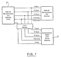
- a conventional CRT controller shown as an IBM PC (Personal Computer) monochrome CRT adapter 21 has the following basic outputs; VIDEO, VSYNC, HSYNC and INTENSITY signals.
- the clock signal shown in Fig. 1 is a signal required by the gas panel monitor 27.
- the gas panel monitor 27 like a CRT monitor, operates in a horizontal scanning mode and utilises the same signal train to generate the display. Characters tagged for highlighting (in the sense of rendering distinctive) are reduced in brightness by skipping every other frame and interlacing both vertically and horizontally to handle flicker.
- a panel line can be updated by erasing and then selectively writing the video data or by writing all cells followed by selectively erasing.
- the latter method is employed in the described embodiment of the invention as it produces less crosstalk and improves the panel's operating ranges.
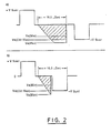
- Figure 2 illustrates two species of erase waveform appropriate to the IBM (R.T.M.) 3290 and 581 Plasma Display Assemblies, which are large size high resolution commercially available plasma display panels having a line resolution of 72 lines per inch and 960 x 768 pels (picture elements) in conventional and, potentially, in video mode.
- a 720 x 350 section of the panel is driven by CRT monochrome adapter 21 and refreshed at a 50 frame per second rate with 3 intensity levels, normal, dim and off.
- Section a of Figure 2 illustrates the conventional erase waveform used in the IBM 3290 Information Processor and the IBM 581 Plasma Display Subassembly (PDSA).
- This erase waveform was designed to maximise write and erase operating ranges under widely varying image sequences that can occur in random X, Y addressing mode, especially in a highly interactive environment. Every erase cycle, shown as the 16.5 microsecond crosshatched waveform is followed by a short burst of sustain cycles shown as +V SUST and -V SUST, to minimise or buffer the effect of the long erase cycle on the sustain function, since consecutive erase cycles take over 90 microseconds. Such time is not available for a non-interlaced video mode operation so that a faster erase waveform is required.
- Video mode using a conventional raster scan technique, does not produce the widely varying image sequences that are available in XY addressing mode. Therefore, the write and erase waveforms can be modified without degrading the operating ranges.
- the conventional plasma display erase waveform is wide and operates over a large voltage range. Though it is not normally used at sustain amplitude (approximately 90 volts), it functions well at this amplitude, and the flat portion of the erase pulse can be seen to be identical to the sustain alternation that it precedes.
- Section b of Figure 2 illustrates the modified erase waveform used to speed up the erase operation.
- the rise time is faster and the flat sustain like portion of the conventional erase pulse is eliminated.
- the crosshatched triangular leading edge is not present, leaving a normal sustain alternation; when a cell is selected to erase, the presence of the triangular leading edge creates a waveform almost identical to the old erase waveform at sustain amplitude.
- the new waveform functions like the old waveform, but is much shorter in duration. Reducing the width of the erase pulse from 16.5 to approximately 6 microseconds permitted operating in video mode.
- the two sustain cycles within the 54 microseconds establishes a 37 kHz sustain frequency, only 3 kHz lower than the 40 kHz optimum sustain frequency for these panels.
- the sustain cycles previously required between consecutive write or erase operations were also eliminated.
- the NRZ transition reduces the tendency of the write pulse to self erase at high write amplitude.
- the NRZ transition represents an engineering compromise which is not quite as effective as the post write pedestal in eliminating self erase, but allows for a much shorter write operation.
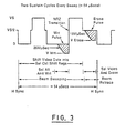
- the sustain, write and erase operations are continuous, and are synchronised to the H signals and to the video data as shown in Figure 3.
- the first horizontal sweeps in a frame are not accompanied by video data, and therefore write and erase pulses are not generated.
- the waveforms of Figure 3 are generated with time allotted for the non existent write and erase pulses. A few sweeps later, when video data is present, the write and erase pulses are generated to update the panel lines. For convenience, alternate odd and even lines are driven from opposite sides of the panel so that two shift registers for each axis are used to store the contents of the display being generated.
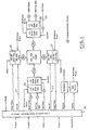
- the frame sequence starts with a V SYNC signal applied to the video control unit 31.
- all cells of the upper two panel lines 1 and 2 are selected by single one bits shifted into both horizontal selection circuit shift registers 33 and 35.
- the right (even) SEL NONE line 37 is then used to deselect line 2, leaving line 1 (odd) selected.
- Vertical "SEL ALL" lines 41, 43 are used to select all vertical lines and all cells of line 1 are turned on by writing. This completes frame initialisation and the logic waits for the first active H sweep with all cells on line 1 lit.
- Consecutive horizontal line pairs (1/2, 2/3, 3/4 etc.) are selected by alternately shifting the single one bit in either the left or the right shift register, after each horizontal sweep.
- next horizontal sequence therefore turns on all the cells on line 3 and then selectively erase line 2. This horizontal sequence continues down the entire panel until one entire frame of video data is written and displayed.
- the next V SYNC signal occurs, the next frame is initialised, as described above, and the entire sequence is repeated 50 times a second.
- border pilot cells are generally employed to initially light the panel from a power-on start and to condition the cells for discharge in a write operation.
- pilot cells are not required, and the expense of pilot line driver circuits and the panel area needed for the pilot lines are not required.
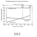
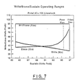
- Figures 5 through 7 represent typical plots of write, erase and sustain operating ranges used in AC plasma panel operated in video mode. Experimental panels were made with chamber gaps from 3 to 4 mils, and resolution from 72 lines per inch to 105 lines per inch. Each plot in Figures 5 through 7 represents the operating parameters for a specified panel tested in both XY addressing and video modes. The only significant difference in operating parameters for a panel tested in both modes is the panels VS(MAX). Therefore, for simplification, the sustain write and erase minimums have been normalised and are shown as coincident, and the two VS (MAX) points are labelled to illustrate the difference.
- VS(MAX) is one of the components of the operating margin of a panel, which margin is defined as the difference between the maximum sustain voltage VS(MAX) and the minimum sustain voltage VS(MIN), or (VS(MAX) - VS(MIN)).
- an ACPDP can be used to replace a CRT as a display component in a computer terminal or monitor.
- the ACPDP operates better than it does in the X, Y random address mode and has the following advantages:
Landscapes
- Engineering & Computer Science (AREA)
- Physics & Mathematics (AREA)
- Power Engineering (AREA)
- Plasma & Fusion (AREA)
- Computer Hardware Design (AREA)
- General Physics & Mathematics (AREA)
- Theoretical Computer Science (AREA)
- Control Of Indicators Other Than Cathode Ray Tubes (AREA)
- Transforming Electric Information Into Light Information (AREA)
Claims (3)
- Dispositif d'affichage à balayage de trame, du type dans lequel l'affichage est produit, d'une manière progressive à l'intérieur de lignes de zones d'affichage et progressivement pour chaque ligne dans une direction donnée, à partir d'un flux de données d'entrée, et l'élément d'affichage est un dispositif d'affichage à plasma possédant une matrice de cellules d'affichage, organisée suivant des lignes et des colonnes, caractérisé en ce qu'il est prévu des moyens pour exciter un couple de lignes de cellules, proches, le couple de lignes s'étendant dans la direction donnée, et pour éteindre de façon sélective des cellules situées dans la ligne précédente du couple en correspondance avec la section du flux de données d'entrée, voisine de cette ligne.
- Dispositif d'affichage à balayage de trame selon la revendication 1, dans lequel les lignes voisines sont directement adjacentes et les cellules pilotes classiques d'un élément d'affichage à plasma sont supprimées de l'élément d'affichage à plasma incorporé.
- Procédé pour produire un affichage à balayage de trame dans un élément d'affichage à plasma, qui comporte une matrice de cellules d'affichage organisées suivant des lignes et des colonnes et incluant l'alignement des lignes du balayage de trame avec les lignes de la matrice de cellules, l'excitation de toutes les cellules dans la ligne de cellules correspondant à la ligne actuelle de balayage de trame ainsi que toutes les cellules situées dans une ligne de cellules, au voisinage de cette dernière, mais en correspondance avec une ligne de balayage de trame non encore atteinte lors du balayage de trame, et l'extinction des cellules de la ligne de cellules, qui correspondent à la ligne actuelle de balayage de trame et qui ne doivent pas rester obligatoirement excitées pour l'affichage de données.
Applications Claiming Priority (2)
| Application Number | Priority Date | Filing Date | Title |
|---|---|---|---|
| US06/591,099 US4611203A (en) | 1984-03-19 | 1984-03-19 | Video mode plasma display |
| US591099 | 1984-03-19 |
Publications (3)
| Publication Number | Publication Date |
|---|---|
| EP0155488A2 EP0155488A2 (fr) | 1985-09-25 |
| EP0155488A3 EP0155488A3 (en) | 1988-11-30 |
| EP0155488B1 true EP0155488B1 (fr) | 1991-06-19 |
Family
ID=24365057
Family Applications (1)
| Application Number | Title | Priority Date | Filing Date |
|---|---|---|---|
| EP85101321A Expired EP0155488B1 (fr) | 1984-03-19 | 1985-02-08 | Méthode et dispositif d'affichage à balayage à trame |
Country Status (4)
| Country | Link |
|---|---|
| US (1) | US4611203A (fr) |
| EP (1) | EP0155488B1 (fr) |
| JP (1) | JPH0677183B2 (fr) |
| DE (1) | DE3583251D1 (fr) |
Families Citing this family (46)
| Publication number | Priority date | Publication date | Assignee | Title |
|---|---|---|---|---|
| DE3486401T2 (de) * | 1983-12-09 | 1996-01-04 | Fujitsu Ltd | Verfahren zur Steuerung einer Gasentladungsanzeigevorrichtung. |
| JPH0673063B2 (ja) * | 1984-12-18 | 1994-09-14 | 富士通株式会社 | ガス放電パネルの駆動方法 |
| US4683470A (en) * | 1985-03-05 | 1987-07-28 | International Business Machines Corporation | Video mode plasma panel display |
| US4742347A (en) * | 1986-01-17 | 1988-05-03 | International Business Machines Corporation | Refreshing circuit for multi-panel display |
| EP0244978B1 (fr) * | 1986-04-25 | 1992-11-04 | Seiko Instruments Inc. | Interface, par exemple pour un dispositif de visualisation à cristal liquide |
| US4756528A (en) * | 1986-07-24 | 1988-07-12 | Ramon Umashankar | Video system for passenger vehicles |
| US5351064A (en) * | 1987-06-19 | 1994-09-27 | Kabushiki Kaisha Toshiba | CRT/flat panel display control system |
| EP0295692B1 (fr) * | 1987-06-19 | 1994-11-23 | Kabushiki Kaisha Toshiba | Dispositif de commande d'affichage pour un appareil à TRC/plasma |
| DE3852148T2 (de) * | 1987-06-19 | 1995-04-06 | Toshiba Kawasaki Kk | Anzeigemodusumschaltsystem für ein Plasmaanzeigegerät. |
| EP0295690B1 (fr) * | 1987-06-19 | 1994-11-30 | Kabushiki Kaisha Toshiba | Système de commande de la zone de visualisation pour un dispositif d'affichage à plasma |
| DE3853447T2 (de) * | 1987-06-19 | 1995-08-31 | Toshiba Kawasaki Kk | Anzeigesteuergerät für eine Kathodenstrahlröhre-/Plasmaanzeigeeinheit. |
| US4956577A (en) * | 1988-05-10 | 1990-09-11 | Parker William P | Interactive luminous panel display device |
| US5126632A (en) * | 1988-05-10 | 1992-06-30 | Parker William P | Luminous panel display device |
| US4887003A (en) * | 1988-05-10 | 1989-12-12 | Parker William P | Screen printable luminous panel display device |
| US5198723A (en) * | 1988-05-10 | 1993-03-30 | Parker William P | Luminous panel display device |
| EP0344622A3 (fr) * | 1988-05-28 | 1991-07-24 | Kabushiki Kaisha Toshiba | Système de commande d'un panneau d'affichage à plasma |
| JP2892009B2 (ja) * | 1988-05-28 | 1999-05-17 | 株式会社東芝 | 表示制御方式 |
| JP2892010B2 (ja) * | 1988-05-28 | 1999-05-17 | 株式会社東芝 | 表示制御方式 |
| US5293485A (en) * | 1988-09-13 | 1994-03-08 | Kabushiki Kaisha Toshiba | Display control apparatus for converting color/monochromatic CRT gradation into flat panel display gradation |
| KR930000410B1 (ko) * | 1988-09-13 | 1993-01-18 | 가부시기가이샤 도시바 | 컬러/모노크로 crt 계조를 pdp 계조로 변환하는 표시 제어장치 |
| JP2909079B2 (ja) * | 1988-09-13 | 1999-06-23 | 株式会社東芝 | 表示制御方式 |
| JPH02287593A (ja) * | 1989-04-28 | 1990-11-27 | Toshiba Corp | ディスプレイの接続状態判別方式 |
| JPH0362090A (ja) * | 1989-07-31 | 1991-03-18 | Toshiba Corp | フラットパネル表示制御回路 |
| JP2902019B2 (ja) * | 1989-12-05 | 1999-06-07 | 日本放送協会 | 気体放電表示パネルの駆動方法および装置 |
| CA2041819C (fr) * | 1990-05-07 | 1995-06-27 | Hiroki Zenda | Dispositif de commande d'afficheur couleur a cristaux liquides |
| FR2662292B1 (fr) * | 1990-05-15 | 1992-07-24 | Thomson Tubes Electroniques | Procede de reglage de la luminosite d'ecrans de visualisation. |
| JPH06318060A (ja) * | 1991-07-31 | 1994-11-15 | Toshiba Corp | 表示制御装置 |
| US5519414A (en) * | 1993-02-19 | 1996-05-21 | Off World Laboratories, Inc. | Video display and driver apparatus and method |
| JP3025598B2 (ja) * | 1993-04-30 | 2000-03-27 | 富士通株式会社 | 表示駆動装置及び表示駆動方法 |
| US5745086A (en) * | 1995-11-29 | 1998-04-28 | Plasmaco Inc. | Plasma panel exhibiting enhanced contrast |
| JP3028087B2 (ja) * | 1997-07-08 | 2000-04-04 | 日本電気株式会社 | プラズマディスプレイパネルの駆動方法 |
| JP4210805B2 (ja) | 1998-06-05 | 2009-01-21 | 株式会社日立プラズマパテントライセンシング | ガス放電デバイスの駆動方法 |
| JP3424587B2 (ja) * | 1998-06-18 | 2003-07-07 | 富士通株式会社 | プラズマディスプレイパネルの駆動方法 |
| KR100374100B1 (ko) | 1998-09-11 | 2003-04-21 | 엘지전자 주식회사 | 플라즈마표시패널의구동방법 |
| JP3466098B2 (ja) | 1998-11-20 | 2003-11-10 | 富士通株式会社 | ガス放電パネルの駆動方法 |
| US7595774B1 (en) | 1999-04-26 | 2009-09-29 | Imaging Systems Technology | Simultaneous address and sustain of plasma-shell display |
| US7456808B1 (en) | 1999-04-26 | 2008-11-25 | Imaging Systems Technology | Images on a display |
| US6985125B2 (en) | 1999-04-26 | 2006-01-10 | Imaging Systems Technology, Inc. | Addressing of AC plasma display |
| US7619591B1 (en) | 1999-04-26 | 2009-11-17 | Imaging Systems Technology | Addressing and sustaining of plasma display with plasma-shells |
| US7911414B1 (en) | 2000-01-19 | 2011-03-22 | Imaging Systems Technology | Method for addressing a plasma display panel |
| US7157854B1 (en) | 2002-05-21 | 2007-01-02 | Imaging Systems Technology | Tubular PDP |
| US7122961B1 (en) | 2002-05-21 | 2006-10-17 | Imaging Systems Technology | Positive column tubular PDP |
| US8289233B1 (en) | 2003-02-04 | 2012-10-16 | Imaging Systems Technology | Error diffusion |
| US8305301B1 (en) | 2003-02-04 | 2012-11-06 | Imaging Systems Technology | Gamma correction |
| ATE488835T1 (de) | 2005-12-22 | 2010-12-15 | Imaging Systems Technology Inc | Sas-adressierung einer ac-plasmaanzeige mit oberflächenentladung |
| US8248328B1 (en) | 2007-05-10 | 2012-08-21 | Imaging Systems Technology | Plasma-shell PDP with artifact reduction |
Family Cites Families (10)
| Publication number | Priority date | Publication date | Assignee | Title |
|---|---|---|---|---|
| US3940757A (en) * | 1975-02-05 | 1976-02-24 | Autotelic Industries, Ltd. | Method and apparatus for creating optical displays |
| US4176298A (en) * | 1977-05-23 | 1979-11-27 | Modern Controls, Inc. | Display panel apparatus and method of driving |
| US4247854A (en) * | 1979-05-09 | 1981-01-27 | Ncr Corporation | Gas panel with improved circuit for display operation |
| US4352101A (en) * | 1980-06-20 | 1982-09-28 | Lucitron, Inc. | Flat panel display system |
| US4456909A (en) * | 1980-06-30 | 1984-06-26 | Fujitsu Limited | Method and circuit for selectively driving capacitive display cells in a matrix type display |
| JPS57112794A (en) * | 1980-12-29 | 1982-07-13 | Fujitsu Ltd | Driving system for display panel |
| JPS57135991A (en) * | 1981-02-16 | 1982-08-21 | Nippon Electric Co | System of driving external electrode type discharge dispaly panel |
| US4373157A (en) * | 1981-04-29 | 1983-02-08 | Burroughs Corporation | System for operating a display panel |
| DE3228033A1 (de) * | 1982-07-27 | 1984-02-02 | Siteg Siebtechnik GmbH, 4422 Ahaus | Spirale grosser laenge zur herstellung eines spiralbandes und verfahren und vorrichtung zum einbringen von fuellmaterial in diese spiralen |
| JPS5924891A (ja) * | 1982-08-03 | 1984-02-08 | 日本電気株式会社 | 放電表示板の駆動方式 |
-
1984
- 1984-03-19 US US06/591,099 patent/US4611203A/en not_active Expired - Fee Related
- 1984-12-17 JP JP59264689A patent/JPH0677183B2/ja not_active Expired - Lifetime
-
1985
- 1985-02-08 EP EP85101321A patent/EP0155488B1/fr not_active Expired
- 1985-02-08 DE DE8585101321T patent/DE3583251D1/de not_active Expired - Lifetime
Also Published As
| Publication number | Publication date |
|---|---|
| JPH0677183B2 (ja) | 1994-09-28 |
| JPS60208180A (ja) | 1985-10-19 |
| US4611203A (en) | 1986-09-09 |
| EP0155488A3 (en) | 1988-11-30 |
| EP0155488A2 (fr) | 1985-09-25 |
| DE3583251D1 (de) | 1991-07-25 |
Similar Documents
| Publication | Publication Date | Title |
|---|---|---|
| US4611203A (en) | Video mode plasma display | |
| EP0864141B1 (fr) | Ecran a plasma a contraste renforce | |
| KR100917371B1 (ko) | 플라즈마 디스플레이 패널의 구동 방법 및 플라즈마 디스플레이 장치 | |
| EP0810577B1 (fr) | Méthode et dispositif de commande d'un panneau à plasma | |
| US5075597A (en) | Method for the row-by-row control of a coplanar sustaining ac type of plasma panel | |
| US6107978A (en) | Plasma display having variable scan line pulses to reduce flickering | |
| US4683470A (en) | Video mode plasma panel display | |
| KR100764347B1 (ko) | Ac형 pdp의 구동 방법 및 구동 장치 | |
| US4140945A (en) | Sustainer wave form having enhancement pulse for increased brightness in a gas discharge device | |
| JPH10301528A5 (fr) | ||
| US5430458A (en) | System and method for eliminating flicker in displays addressed at low frame rates | |
| US5250936A (en) | Method for driving an independent sustain and address plasma display panel to prevent errant pixel erasures | |
| EP0745251B1 (fr) | Formes d'ondes de tension de commande pour des affichages a cristaux liquides adresses par plasma | |
| US4090109A (en) | Gas discharge coupling of driving circuitry to a gas discharge display/memory panel | |
| KR20020090326A (ko) | 플라즈마디스플레이패널 및 그 구동방법 | |
| KR100648879B1 (ko) | 플라즈마 디스플레이 장치 및 플라즈마 디스플레이 장치에사용되는 구동방법 | |
| US7639212B2 (en) | Ac-type gas-discharge display device | |
| KR0149212B1 (ko) | 피디피의 구동장치와 그 스캔방법 | |
| US4188566A (en) | Method for detecting coordinates of gas discharge panels and apparatus for carrying out the same | |
| KR100697890B1 (ko) | 플라즈마 디스플레이 패널 구동방법 | |
| KR0149218B1 (ko) | 피디피의 스캔방법 | |
| JPS62215294A (ja) | ガス放電パネルの駆動方法 |
Legal Events
| Date | Code | Title | Description |
|---|---|---|---|
| PUAI | Public reference made under article 153(3) epc to a published international application that has entered the european phase |
Free format text: ORIGINAL CODE: 0009012 |
|
| AK | Designated contracting states |
Designated state(s): DE FR GB |
|
| 17P | Request for examination filed |
Effective date: 19860124 |
|
| PUAL | Search report despatched |
Free format text: ORIGINAL CODE: 0009013 |
|
| AK | Designated contracting states |
Kind code of ref document: A3 Designated state(s): DE FR GB |
|
| 17Q | First examination report despatched |
Effective date: 19901002 |
|
| GRAA | (expected) grant |
Free format text: ORIGINAL CODE: 0009210 |
|
| AK | Designated contracting states |
Kind code of ref document: B1 Designated state(s): DE FR GB |
|
| REF | Corresponds to: |
Ref document number: 3583251 Country of ref document: DE Date of ref document: 19910725 |
|
| ET | Fr: translation filed | ||
| PLBE | No opposition filed within time limit |
Free format text: ORIGINAL CODE: 0009261 |
|
| STAA | Information on the status of an ep patent application or granted ep patent |
Free format text: STATUS: NO OPPOSITION FILED WITHIN TIME LIMIT |
|
| 26N | No opposition filed | ||
| PGFP | Annual fee paid to national office [announced via postgrant information from national office to epo] |
Ref country code: GB Payment date: 19950125 Year of fee payment: 11 |
|
| PGFP | Annual fee paid to national office [announced via postgrant information from national office to epo] |
Ref country code: FR Payment date: 19950128 Year of fee payment: 11 |
|
| PGFP | Annual fee paid to national office [announced via postgrant information from national office to epo] |
Ref country code: DE Payment date: 19950223 Year of fee payment: 11 |
|
| PG25 | Lapsed in a contracting state [announced via postgrant information from national office to epo] |
Ref country code: GB Effective date: 19960208 |
|
| GBPC | Gb: european patent ceased through non-payment of renewal fee |
Effective date: 19960208 |
|
| PG25 | Lapsed in a contracting state [announced via postgrant information from national office to epo] |
Ref country code: FR Effective date: 19961031 |
|
| PG25 | Lapsed in a contracting state [announced via postgrant information from national office to epo] |
Ref country code: DE Effective date: 19961101 |
|
| REG | Reference to a national code |
Ref country code: FR Ref legal event code: ST |