EP0156502B1 - Montage de dispositifs à ondes acoustiques de surface - Google Patents
Montage de dispositifs à ondes acoustiques de surface Download PDFInfo
- Publication number
- EP0156502B1 EP0156502B1 EP85301141A EP85301141A EP0156502B1 EP 0156502 B1 EP0156502 B1 EP 0156502B1 EP 85301141 A EP85301141 A EP 85301141A EP 85301141 A EP85301141 A EP 85301141A EP 0156502 B1 EP0156502 B1 EP 0156502B1
- Authority
- EP
- European Patent Office
- Prior art keywords
- substrate
- saw
- leads
- gold
- propagating
- Prior art date
- Legal status (The legal status is an assumption and is not a legal conclusion. Google has not performed a legal analysis and makes no representation as to the accuracy of the status listed.)
- Expired - Lifetime
Links
Images


Classifications
-
- H—ELECTRICITY
- H03—ELECTRONIC CIRCUITRY
- H03H—IMPEDANCE NETWORKS, e.g. RESONANT CIRCUITS; RESONATORS
- H03H3/00—Apparatus or processes specially adapted for the manufacture of impedance networks, resonating circuits, resonators
- H03H3/007—Apparatus or processes specially adapted for the manufacture of impedance networks, resonating circuits, resonators for the manufacture of electromechanical resonators or networks
- H03H3/08—Apparatus or processes specially adapted for the manufacture of impedance networks, resonating circuits, resonators for the manufacture of electromechanical resonators or networks for the manufacture of resonators or networks using surface acoustic waves
-
- H—ELECTRICITY
- H03—ELECTRONIC CIRCUITRY
- H03H—IMPEDANCE NETWORKS, e.g. RESONANT CIRCUITS; RESONATORS
- H03H9/00—Networks comprising electromechanical or electro-acoustic elements; Electromechanical resonators
- H03H9/25—Constructional features of resonators using surface acoustic waves
-
- Y—GENERAL TAGGING OF NEW TECHNOLOGICAL DEVELOPMENTS; GENERAL TAGGING OF CROSS-SECTIONAL TECHNOLOGIES SPANNING OVER SEVERAL SECTIONS OF THE IPC; TECHNICAL SUBJECTS COVERED BY FORMER USPC CROSS-REFERENCE ART COLLECTIONS [XRACs] AND DIGESTS
- Y10—TECHNICAL SUBJECTS COVERED BY FORMER USPC
- Y10T—TECHNICAL SUBJECTS COVERED BY FORMER US CLASSIFICATION
- Y10T29/00—Metal working
- Y10T29/42—Piezoelectric device making
-
- Y—GENERAL TAGGING OF NEW TECHNOLOGICAL DEVELOPMENTS; GENERAL TAGGING OF CROSS-SECTIONAL TECHNOLOGIES SPANNING OVER SEVERAL SECTIONS OF THE IPC; TECHNICAL SUBJECTS COVERED BY FORMER USPC CROSS-REFERENCE ART COLLECTIONS [XRACs] AND DIGESTS
- Y10—TECHNICAL SUBJECTS COVERED BY FORMER USPC
- Y10T—TECHNICAL SUBJECTS COVERED BY FORMER US CLASSIFICATION
- Y10T29/00—Metal working
- Y10T29/49—Method of mechanical manufacture
- Y10T29/49002—Electrical device making
- Y10T29/49117—Conductor or circuit manufacturing
- Y10T29/49124—On flat or curved insulated base, e.g., printed circuit, etc.
- Y10T29/4913—Assembling to base an electrical component, e.g., capacitor, etc.
- Y10T29/49144—Assembling to base an electrical component, e.g., capacitor, etc. by metal fusion
Definitions
- This invention relates to the construction and mounting of surface acoustic wave (SAW) devices.
- SAW surface acoustic wave
- SAW devices are used for example as bandpass filters in conjunction with electronic circuits.
- a typical known SAW device comprises a rectangular substrate of quartz on the surface of which are formed metal electrodes. These electrodes can be connected to a circuit by appropriate leads.
- the substrate is mounted upon a metal support to which it is bonded by an organic adhesive.
- the organic adhesive is usually formed round the end of the substrate to act as an acoustic absorber to reduce acoustic reflections from the end faces of the quartz.
- the use of metal mounted packages is not practical for thick film circuit boards with surface mounted components. It is possible to laser drill mounting holes in the thick film board for these metal packages but this is expensive.
- the present invention is concerned with a method for mounting SAW devices which does not make use of organic bonding agents, and which allows the completed devices to be mounted directly onto a hybrid circuit.
- a method of mounting a surface acoustic wave (SAW) device comprising a SAW-propagating first substrate onto a second substracte having conductive regions thereon, the SAW device further comprising metallised areas including SAW transducer elements and bond pads disposed on one face of the SAW-propagating first substrate, the method comprising the steps of attaching conductive leads to the bond pads, positioning the SAW device face down over, and in immediate proximity to, the second substrate, and attaching the conductive leads to the conductive regions of the second substrate, so that the leads run substantially parallel to said face of the first substrate.
- SAW surface acoustic wave
- the conductive leads are attached to the conductive regions of the second substrate in such a manner that the first substrate is supported on the leads at a distance of the order of magnitude of the thickness of the leads away from the second substrate.
- the method may include the steps of forming a plurality of said metallised areas on a piece of material suitable for forming SAW devices, and then cutting said material into individual devices prior to attachment to said leads.
- a particularly advantageous shape for the SAW substrate has been found to be generally diamond shaped. If this shape is employed the need for an acoustic absorber at the ends of the device is avoided.
- the leads can be attached to the metallised areas by thermo-compression bonding.
- the leads can also be attached to the conductive regions of the second substrate by thermo-compression bonding.
- the second substrate may be a hybrid circuit.
- the metallisation areas of the SAW substrate may include an aluminium layer and a gold layer.
- a titanium layer is formed between the aluminium and gold layers to prevent aluminiun-gold interdiffusion.
- the leads and the conductive regions on the second substrate may be formed from gold.
- the SAW substrate may be formed from quartz.
- the devices formed by the present method are particularly suitable for use with thick and thin film hybrid circuits.
- a hybrid circuit including a surface acoustic wave (SAW) device mounted on a supporting substrate, wherein the SAW device comprises a SAW-propagating substrate having metallised areas including SAW transducer elements and bond pads disposed on one face thereof, and conductive leads attached directly to the bond pads and arranged to run substantially parallel and in immediate proximity to said one face, and wherein the SAW-propagating substrate is secured to the supporting substrate by attaching the conductive leads to conductive regions on the supporting substrate such that the SAW-propagating substrate is supported by the leads in a substantially stress-free manner, with the transducer face in immediate proximity to the supporting substrate, and without the need for organic bonding agents for securing the device.
- SAW surface acoustic wave
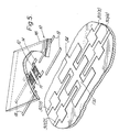
- the first step is to form a plurality of metallised areas on the surface of a slab of quartz shown generally at 10.
- Figure 1 there is shown only an area corresponding substantially to a single SAW device, but it will be appreciated that the slab 10 is considerably larger than the area shown, so that metallised areas for several SAW devices can be formed at the same time.
- the metallised areas are shown at 11 at Figure 1.
- Each metallised area 11 comprises an L-shaped layer 12 formed of aluminium, and a bond pad in the form of a rectangular layer 14 which partially over-lays one limb of the L-shape.
- the layer 14 is formed of gold
- a layer of titanium is formed intermediate the gold and aluminium to prevent gold-aluminium migration.
- each individual device is illustrated by the line 16 in Figure 1 and can be seen to be a diamond shape.
- Conductive leads are attached to the gold bonding areas on the surface of each device as shown in Figure 2 of the drawings.
- the conductive leads are shown by reference numeral 18 and are attached to each gold bonding area by thermo-compression bonding as described below. Typical dimensions for each device can be seen on Figure 1 of the drawings.
- each SAW device can then be mounted on a hybrid circuit board as follows.
- the device is inverted so that the surface to which the leads 18 have been attached is facing downwardly.
- the device is located over a hybrid circuit board which has a conductor pattern as shown in Figures 4 and 5 of the drawings.
- the device is placed upon the circuit board so that the leads 18 are supported on the conductive regions shown at 30.
- Figure 3 of the drawings it will be seen that the leads 18 are in face to face contact with the conductors 30 and are supported thereby.
- the leads 18 are attached to the conductors 30 by thermo-compression bonding to form the completed arrangement.
- the present technique has a number of advantages over the prior art.
- the diamond shape substrate can reduce end reflections without the need for providing any acoustic damping material at the ends of the substrate.
- the technique of using tape bonding to attach the device to the circuit board results in a low profile device and this helps in conjunction with the conductor arrangement shown in Figure 4 to reduce electromagnetic breakthrough between SAW transducers.
- the leads can be formed in such a way that no stress is transmitted from the hybrid substrate to the quartz substrate.
- the area shown by reference numeral 34 is an earth shield which helps to reduce the electromagnetic breakthrough referred to above.
- a major feature of the present method is that it does not make use of any organic bonding agents in any form. Thus, the problem of out-gassing from such compounds does not occur and enables the SAW device to be mounted directly on the hybrid circuit board.
- the mounting method also reduces the stresses applied to the quartz substrate during its operational life.
- organic compounds hold the SAW device in a rigid manner. This does not allow for thermal expansion of the substrate relative to the metal package. Such a problem is not so marked in the present arrangement.
- the SAW substrate 10 is supported mainly at areas corresponding to the metallised areas 11. This provides a relatively stress-free mounting which should reduce the ageing of the SAW device and possibly improve its long term reliability.
- the SAW filters fabricated by the present applicants are made on 1 mm thick, natural quartz cut in the ST plane.
- the interdigitated transducers are printed and etched in a 150 nm thick aluminium metallisation using optical photoengraving techniques.
- the titanium/gold bond pads are defined on top of the aluminium fingers using a lift off process such as described, for example, by FRARY, J M and SESSE, P: 'Lift-off Techniques for Fine Line Metal Patterning', Semiconductor International, Dec. 1981, pp. 72-88.
- the quartz is separated into individual devices by sawing completely through the substrate with a diamond blade. As mentioned above, in order to minimise the effect of edge reflections the quartz is sawn into diamond shaped chips. Acoustic waves travelling towards the apexes of the chip are greatly damped by multiple reflections between the converging edges.
- Gold tape of 99.99% purity measuring 0.075 mm thick and 0.375 mm wide was used for the leads. Tape lengths of 3 mm were cut and then annealed in air for 15 minutes at 800 o C immediately before use.
- the chip was then placed acoustic face down onto the hybrid, with the ends of the gold leads over the thick gold bonding lands.
- the hybrid was clamped to the heated chuck of the bonding machine and the leads bonded to the thick film, again using the pointed bonding tool that was used to attach the leads to the SAW chip.
- the pointed bonding tool that was used to attach the leads to the SAW chip.
- the transducers with titanium/gold bond pads were tested mechanically and gave gold lead pull strengths in excess of 0.5 N and failure of these devices was due to lead breakage.
- gold leads could be bonded directly to aluminium bonding pads on the SAW chip, the pull strength of the leads was only a few grams and failure occured by the aluminium metal lifting from the quartz substrate.
- Assembled SAW devices with titanium/gold bond pads have been subjected to 1000 shocks at 2000 g and 1 minute vibration at 180 Hz (20 g amplitude) without failure.
- Mounting the SAW devices by the method of the invention also offers improvements in the performance of the SAW devices.
- the use of low profile bonding leads reduces electromagnetic breakthrough and secondly the earth plane on the thick film circuit can be positioned very close to the transducers to provide excellent screening.
- An overall improvement of 10 dB in the stopband rejection of SAW filters so mounted was achieved.
- the ripple introduced into the amplitude response was approximately +/- 0.05 dB.
Landscapes
- Physics & Mathematics (AREA)
- Acoustics & Sound (AREA)
- Engineering & Computer Science (AREA)
- Manufacturing & Machinery (AREA)
- Surface Acoustic Wave Elements And Circuit Networks Thereof (AREA)
Claims (18)
- Un procédé de montage d'un dispositif d'ondes acoustiques de surface (SAW) comprenant un premier substrat (16) de propagation de SAW sur un deuxième substrat portant des régions conductrices (30), le dispositif SAW comprenant en outre des zones métallisées (11, 12, 14) comprenant des éléments transducteurs de SAW et des pastilles d'attache disposées sur une face du premier substrat de propagation des SAW, le procédé comprenant les étapes consistant à attacher des fils conducteurs (18) sur les pastilles d'attache, positionner le dispositif de SAW retourné face vers le bas au-dessus du deuxième substrat, et à proximité immédiate de celui-ci, et à attacher les fils conducteurs (18) sur les régions conductrices (30) du deuxième substrat, de façon que les fils courent sensiblement en parallèle à ladite face dudit premier substrat.
- Un procédé selon la revendication 1, dans lequel les fils conducteurs sont attachés aux régions conductrices du deuxième substrat d'une manière telle que le premier substrat est supporté sur les fils à l'écart du deuxième substrat, à une distance de l'ordre de grandeur de l'épaisseur des fils.
- Un procédé selon la revendication 1 ou la revendication 2, comprenant en outre les étapes consistant à former plusieurs desdites zones métallisées sur un élément en matière appropriée pour former des dispositifs de SAW, et à couper ensuite ladite matière en dispositifs individuels avant de l'attacher sur lesdits fils.
- Un procédé selon l'une quelconque des revendications 1 à 3, comprenant en outre l'étape consistant à former un substrat de SAW qui est en forme générale de losange.
- Un procédé selon l'une quelconque des revendications 1 à 4, dans lequel les fils sont attachés aux pastilles d'attache par une soudure par thermocompression.
- Un procédé selon l'une quelconque des revendications 1 à 5, dans lequel les fils sont attachés aux régions conductrices du deuxième substrat par soudure par thermocompression.
- Un procédé selon l'une quelconque des revendications 1 à 6, dans lequel le deuxième substrat est un circuit hybride.
- Un procédé selon l'une quelconque des revendications 1 à 7, dans lequel les zones métallisées du substrat de SAW comprennent une couche (12) d'aluminium et une couche (14) d'or.
- Un procédé selon la revendication 8, dans lequel une couche de titane est formée entre les couches d'aluminium et d'or pour empêcher une interdiffusion aluminium-or.
- Un procédé selon l'une quelconque des revendications 1 à 9, dans lequel les fils et les régions conductrices du deuxième substrat sont en or.
- Un procédé selon l'une quelconque des revendications 1 à 10, dans lequel le substrat de SAW est en quartz.
- Un circuit hybride comprenant un dispositif (16) d'ondes acoustiques de surface (SAW) monté sur un substrat de support, dans lequel le dispositif de SAW comprend un substrat (16) de propagation de SAW, portant, sur une première face, des zones métallisées (11, 12, 14) comprenant des éléments transducteurs de SAW et des pastilles d'attache, et comportant des fils conducteurs (18) attachés directement sur les pastilles (14) d'attache et disposés de façon à courir sensiblement en parallèle à ladite première face et à proximité immédiate de celle-ci, et dans lequel le substrat (16) de propagation de SAW est fixé au substrat de support en attachant les fils conducteurs (18) à des régions conductrices (30) sur le substrat de support d'une façon telle que le substrat de propagation de SAW est supporté par les fils d'une manière sensiblement exempte de contraintes, la face du transducteur étant à proximité immédiate du substrat de support, et sans que des agents organiques d'attache ne soient nécessaires pour fixer le dispositif.
- Un circuit hybride selon la revendication 12, dans lequel le substrat de propagation de SAW est sensiblement en forme de losange, et les éléments transducteurs sont disposés de façon orthogonale à une diagonale entre les pointes de la forme de losange d'une manière telle que, en fonctionnement, le SAW se propage sensiblement le long de ladite diagonale, et que des réflexions indésirables de bords sont atténuées.
- Un circuit hybride selon la revendication 12 ou la revendication 13, dans lequel les zones métallisées du substrat de propagation de SAW comprennent une couche (12) d'aluminium et une couche (14) d'or.
- Un circuit hybride selon la revendication 14, dans lequel une couche de titane est formée entre les couches d'aluminium et d'or sur le substrat de propagation de SAW pour empêcher une interdiffusion aluminium-or.
- Un circuit hybride selon l'une quelconque des revendications 12 à 15, dans lequel les fils conducteurs (18) sont en ruban d'or, et le dispositif de SAW est supporté sur les fils à l'écart du substrat de support, à une distance de l'ordre de grandeur de l'épaisseur du ruban.
- Un circuit hybride selon l'une quelconque des revendications 12 à 16, dans lequel le substrat de propagation de SAW comprend du quartz.
- Un circuit hybride selon l'une quelconque des revendications 12 à 17, dans lequel la face de transducteur du dispositif de SAW est positionnée immédiatement au-dessus d'une région (34) formant écran de masse du substrat de support.
Priority Applications (1)
| Application Number | Priority Date | Filing Date | Title |
|---|---|---|---|
| AT85301141T ATE69916T1 (de) | 1984-02-20 | 1985-02-20 | Montage von akustischen oberflaechenwelleneinrichtungen. |
Applications Claiming Priority (4)
| Application Number | Priority Date | Filing Date | Title |
|---|---|---|---|
| GB8404398 | 1984-02-20 | ||
| GB848404398A GB8404398D0 (en) | 1984-02-20 | 1984-02-20 | Mounting of saw devices |
| GB848423857A GB8423857D0 (en) | 1984-09-20 | 1984-09-20 | Mounting of saw devices |
| GB8423857 | 1984-09-20 |
Publications (2)
| Publication Number | Publication Date |
|---|---|
| EP0156502A1 EP0156502A1 (fr) | 1985-10-02 |
| EP0156502B1 true EP0156502B1 (fr) | 1991-11-27 |
Family
ID=26287340
Family Applications (1)
| Application Number | Title | Priority Date | Filing Date |
|---|---|---|---|
| EP85301141A Expired - Lifetime EP0156502B1 (fr) | 1984-02-20 | 1985-02-20 | Montage de dispositifs à ondes acoustiques de surface |
Country Status (6)
| Country | Link |
|---|---|
| US (2) | US4795934A (fr) |
| EP (1) | EP0156502B1 (fr) |
| CA (1) | CA1281810C (fr) |
| DE (1) | DE3584732D1 (fr) |
| DK (1) | DK475985A (fr) |
| WO (1) | WO1985003815A1 (fr) |
Families Citing this family (11)
| Publication number | Priority date | Publication date | Assignee | Title |
|---|---|---|---|---|
| DE3606214A1 (de) * | 1986-02-26 | 1987-08-27 | Siemens Ag | Halterung des substratplaettchens eines oberflaechenwellen-bauelementes |
| JP2673993B2 (ja) * | 1990-07-02 | 1997-11-05 | 日本無線株式会社 | 表面弾性波装置 |
| US6002252A (en) * | 1991-05-22 | 1999-12-14 | Wolff Controls Corporation | Compact sensing apparatus having transducer and signal conditioner with a plurality of mounting pins |
| US5237235A (en) * | 1991-09-30 | 1993-08-17 | Motorola, Inc. | Surface acoustic wave device package |
| US5453652A (en) * | 1992-12-17 | 1995-09-26 | Matsushita Electric Industrial Co., Ltd. | Surface acoustic wave device with interdigital transducers formed on a holding substrate thereof and a method of producing the same |
| US5459368A (en) * | 1993-08-06 | 1995-10-17 | Matsushita Electric Industrial Co., Ltd. | Surface acoustic wave device mounted module |
| US5939817A (en) * | 1994-09-22 | 1999-08-17 | Nippon Electric Co | Surface acoustic wave device |
| JP3301262B2 (ja) * | 1995-03-28 | 2002-07-15 | 松下電器産業株式会社 | 弾性表面波装置 |
| JPH0969748A (ja) * | 1995-09-01 | 1997-03-11 | Matsushita Electric Ind Co Ltd | Sawデバイスおよびその製造方法 |
| US6110761A (en) * | 1997-08-05 | 2000-08-29 | Micron Technology, Inc. | Methods for simultaneously electrically and mechanically attaching lead frames to semiconductor dice and the resulting elements |
| KR100418550B1 (ko) * | 1998-12-29 | 2004-02-11 | 가부시끼가이샤 도시바 | 탄성표면파 장치 |
Family Cites Families (26)
| Publication number | Priority date | Publication date | Assignee | Title |
|---|---|---|---|---|
| US3353263A (en) * | 1964-08-17 | 1967-11-21 | Texas Instruments Inc | Successively stacking, and welding circuit conductors through insulation by using electrodes engaging one conductor |
| US3457639A (en) * | 1967-02-16 | 1969-07-29 | Bell Telephone Labor Inc | Method for alignment of microcircuit devices on substrate |
| US3488530A (en) * | 1968-04-22 | 1970-01-06 | North American Rockwell | Piezoelectric microresonator |
| US3612922A (en) * | 1970-11-10 | 1971-10-12 | Gen Motors Corp | Method of mounting a piezoelectric device |
| US3872410A (en) * | 1972-12-04 | 1975-03-18 | Gte Laboratories Inc | Surface wave filter for tv if stage |
| US3885173A (en) * | 1973-10-09 | 1975-05-20 | Magnavox Co | Apparatus and method for coupling an acoustical surface wave device to an electronic circuit |
| GB1512593A (en) * | 1975-03-13 | 1978-06-01 | Murata Manufacturing Co | Elastic surface wave filter |
| DE2918952C2 (de) * | 1979-05-10 | 1982-10-28 | Siemens AG, 1000 Berlin und 8000 München | Elektrische Baugruppe |
| US4266157A (en) * | 1979-05-18 | 1981-05-05 | The United States Of America As Represented By The Secretary Of The Army | Piezoelectric resonator assembly with thin molybdenum mounting clips |
| JPS5694815A (en) * | 1979-12-28 | 1981-07-31 | Matsushita Electric Ind Co Ltd | Elastic surface wave device |
| JPS56168418A (en) * | 1980-05-29 | 1981-12-24 | Matsushita Electric Ind Co Ltd | Quartz oscillator |
| JPS5745955A (en) * | 1980-09-02 | 1982-03-16 | Seikosha Co Ltd | Sealing container |
| JPS5757018A (en) * | 1980-09-24 | 1982-04-06 | Fujitsu Ltd | Surface acoustic wave filter |
| JPS5757020A (en) * | 1980-09-24 | 1982-04-06 | Fujitsu Ltd | Surface acoustic wave filter |
| JPS5763917A (en) * | 1980-10-06 | 1982-04-17 | Toshiba Corp | Surface wave filter device |
| DE3038261A1 (de) * | 1980-10-10 | 1982-04-29 | Standard Elektrik Lorenz Ag, 7000 Stuttgart | Baueinheit mit piezoelektrischen resonatoren |
| US4396140A (en) * | 1981-01-27 | 1983-08-02 | Bell Telephone Laboratories, Incorporated | Method of bonding electronic components |
| US4398117A (en) * | 1981-03-23 | 1983-08-09 | Sperry Corporation | Bellows support for surface acoustic wave device |
| JPS5883420A (ja) * | 1981-11-13 | 1983-05-19 | Hitachi Ltd | 弾性境界波装置 |
| JPS58133021A (ja) * | 1982-02-02 | 1983-08-08 | Citizen Watch Co Ltd | 弾性表面波装置 |
| DE3377043D1 (en) * | 1982-02-22 | 1988-07-14 | Fujitsu Ltd | Piezoelectric resonators |
| JPS58139513A (ja) * | 1982-05-11 | 1983-08-18 | Murata Mfg Co Ltd | チップ状圧電振動部品の製造方法 |
| JPS58139514A (ja) * | 1982-05-18 | 1983-08-18 | Murata Mfg Co Ltd | チップ状圧電振動部品の製造方法 |
| JPS59148419A (ja) * | 1983-02-14 | 1984-08-25 | Nec Corp | 厚みすべり圧電振動子 |
| US4494033A (en) * | 1983-03-25 | 1985-01-15 | At&T Technologies, Inc. | Thin lead suspension for a piezoelectric resonator |
| US4546283A (en) * | 1984-05-04 | 1985-10-08 | The United States Of America As Represented By The Secretary Of The Air Force | Conductor structure for thick film electrical device |
-
1985
- 1985-02-19 CA CA000474637A patent/CA1281810C/fr not_active Expired - Lifetime
- 1985-02-20 WO PCT/GB1985/000073 patent/WO1985003815A1/fr not_active Ceased
- 1985-02-20 DE DE8585301141T patent/DE3584732D1/de not_active Expired - Lifetime
- 1985-02-20 EP EP85301141A patent/EP0156502B1/fr not_active Expired - Lifetime
- 1985-10-17 DK DK475985A patent/DK475985A/da unknown
-
1986
- 1986-07-22 US US06/896,092 patent/US4795934A/en not_active Expired - Fee Related
-
1990
- 1990-07-27 US US07/560,299 patent/US5035035A/en not_active Expired - Fee Related
Also Published As
| Publication number | Publication date |
|---|---|
| WO1985003815A1 (fr) | 1985-08-29 |
| US5035035A (en) | 1991-07-30 |
| DK475985D0 (da) | 1985-10-17 |
| DE3584732D1 (de) | 1992-01-09 |
| DK475985A (da) | 1985-10-17 |
| US4795934A (en) | 1989-01-03 |
| CA1281810C (fr) | 1991-03-19 |
| EP0156502A1 (fr) | 1985-10-02 |
Similar Documents
| Publication | Publication Date | Title |
|---|---|---|
| EP0156502B1 (fr) | Montage de dispositifs à ondes acoustiques de surface | |
| US6982475B1 (en) | Hermetic wafer scale integrated circuit structure | |
| US4809135A (en) | Chip carrier and method of fabrication | |
| JP3678148B2 (ja) | 圧電デバイス | |
| US20020033652A1 (en) | Piezoelectric device, manufacturing method therefor, and method for manufacturing piezoelectric oscillator | |
| US6006427A (en) | Chip-on-board printed circuit manufacturing process using aluminum wire bonded to copper pads | |
| JPWO2000033455A1 (ja) | 圧電デバイス及びその製造方法 | |
| KR20180059353A (ko) | 전자 부품 및 그 제조 방법 | |
| EP1458018B1 (fr) | Composant électronique et son procédé de fabrication | |
| JPH06151946A (ja) | 半導体受光素子およびその製造方法 | |
| JP3775433B2 (ja) | 電子部品装置 | |
| JP2003115734A (ja) | 弾性表面波装置とその製造方法 | |
| JP7373305B2 (ja) | 弾性波デバイスおよびその製造方法 | |
| JPH05291864A (ja) | 弾性表面波素子実装回路とその製造方法 | |
| JP7406331B2 (ja) | 電子デバイス、モジュールおよびウエハ | |
| JP7480462B2 (ja) | 圧電デバイスおよびその製造方法 | |
| CN109004084A (zh) | 一种声表面波器件及声表面波器件的制造方法 | |
| JPS61501302A (ja) | Saw素子の取り付け方法およびその構造 | |
| JP4203193B2 (ja) | 半導体素子の実装方法 | |
| JP4085549B2 (ja) | 圧電デバイス及びその製造方法 | |
| GB2276977A (en) | Reducing thermal stress in I.C. chip mountings | |
| JPS62195137A (ja) | 半導体装置 | |
| JP3736226B2 (ja) | Sawデバイス | |
| JP3036291B2 (ja) | 半導体装置の実装構造 | |
| JPS586951B2 (ja) | 電子回路装置 |
Legal Events
| Date | Code | Title | Description |
|---|---|---|---|
| PUAI | Public reference made under article 153(3) epc to a published international application that has entered the european phase |
Free format text: ORIGINAL CODE: 0009012 |
|
| AK | Designated contracting states |
Designated state(s): AT BE CH DE FR GB IT LI LU NL SE |
|
| 17P | Request for examination filed |
Effective date: 19860401 |
|
| 17Q | First examination report despatched |
Effective date: 19880811 |
|
| RAP3 | Party data changed (applicant data changed or rights of an application transferred) |
Owner name: BRITISH TELECOMMUNICATIONSPUBLIC LIMITED COMPANY |
|
| REG | Reference to a national code |
Ref country code: GB Ref legal event code: 732 |
|
| GRAA | (expected) grant |
Free format text: ORIGINAL CODE: 0009210 |
|
| AK | Designated contracting states |
Kind code of ref document: B1 Designated state(s): AT BE CH DE FR GB IT LI LU NL SE |
|
| PG25 | Lapsed in a contracting state [announced via postgrant information from national office to epo] |
Ref country code: SE Effective date: 19911127 Ref country code: NL Effective date: 19911127 Ref country code: LI Effective date: 19911127 Ref country code: IT Free format text: LAPSE BECAUSE OF FAILURE TO SUBMIT A TRANSLATION OF THE DESCRIPTION OR TO PAY THE FEE WITHIN THE PRESCRIBED TIME-LIMIT;WARNING: LAPSES OF ITALIAN PATENTS WITH EFFECTIVE DATE BEFORE 2007 MAY HAVE OCCURRED AT ANY TIME BEFORE 2007. THE CORRECT EFFECTIVE DATE MAY BE DIFFERENT FROM THE ONE RECORDED. Effective date: 19911127 Ref country code: CH Effective date: 19911127 Ref country code: BE Effective date: 19911127 Ref country code: AT Effective date: 19911127 |
|
| REF | Corresponds to: |
Ref document number: 69916 Country of ref document: AT Date of ref document: 19911215 Kind code of ref document: T |
|
| REF | Corresponds to: |
Ref document number: 3584732 Country of ref document: DE Date of ref document: 19920109 |
|
| PG25 | Lapsed in a contracting state [announced via postgrant information from national office to epo] |
Ref country code: GB Effective date: 19920227 |
|
| PG25 | Lapsed in a contracting state [announced via postgrant information from national office to epo] |
Ref country code: LU Free format text: LAPSE BECAUSE OF NON-PAYMENT OF DUE FEES Effective date: 19920229 |
|
| REG | Reference to a national code |
Ref country code: CH Ref legal event code: PL |
|
| EN | Fr: translation not filed | ||
| PG25 | Lapsed in a contracting state [announced via postgrant information from national office to epo] |
Ref country code: FR Effective date: 19920417 |
|
| NLV1 | Nl: lapsed or annulled due to failure to fulfill the requirements of art. 29p and 29m of the patents act | ||
| PLBE | No opposition filed within time limit |
Free format text: ORIGINAL CODE: 0009261 |
|
| STAA | Information on the status of an ep patent application or granted ep patent |
Free format text: STATUS: NO OPPOSITION FILED WITHIN TIME LIMIT |
|
| GBPC | Gb: european patent ceased through non-payment of renewal fee | ||
| PG25 | Lapsed in a contracting state [announced via postgrant information from national office to epo] |
Ref country code: DE Effective date: 19921103 |
|
| 26N | No opposition filed | ||
| REG | Reference to a national code |
Ref country code: FR Ref legal event code: ST |