EP0156648A2 - Circuit arithmétique de convolution pour le traitement numérique de signaux - Google Patents
Circuit arithmétique de convolution pour le traitement numérique de signaux Download PDFInfo
- Publication number
- EP0156648A2 EP0156648A2 EP85302161A EP85302161A EP0156648A2 EP 0156648 A2 EP0156648 A2 EP 0156648A2 EP 85302161 A EP85302161 A EP 85302161A EP 85302161 A EP85302161 A EP 85302161A EP 0156648 A2 EP0156648 A2 EP 0156648A2
- Authority
- EP
- European Patent Office
- Prior art keywords
- addresses
- data
- memory
- counter
- series
- Prior art date
- Legal status (The legal status is an assumption and is not a legal conclusion. Google has not performed a legal analysis and makes no representation as to the accuracy of the status listed.)
- Granted
Links
Images





Classifications
-
- H—ELECTRICITY
- H03—ELECTRONIC CIRCUITRY
- H03H—IMPEDANCE NETWORKS, e.g. RESONANT CIRCUITS; RESONATORS
- H03H17/00—Networks using digital techniques
- H03H17/02—Frequency selective networks
- H03H17/0223—Computation saving measures; Accelerating measures
- H03H17/0238—Measures concerning the arithmetic used
-
- G—PHYSICS
- G06—COMPUTING OR CALCULATING; COUNTING
- G06F—ELECTRIC DIGITAL DATA PROCESSING
- G06F7/00—Methods or arrangements for processing data by operating upon the order or content of the data handled
- G06F7/38—Methods or arrangements for performing computations using exclusively denominational number representation, e.g. using binary, ternary, decimal representation
- G06F7/48—Methods or arrangements for performing computations using exclusively denominational number representation, e.g. using binary, ternary, decimal representation using non-contact-making devices, e.g. tube, solid state device; using unspecified devices
- G06F7/544—Methods or arrangements for performing computations using exclusively denominational number representation, e.g. using binary, ternary, decimal representation using non-contact-making devices, e.g. tube, solid state device; using unspecified devices for evaluating functions by calculation
- G06F7/5443—Sum of products
Definitions
- This invention relates to a convolution arithmetic circuit for a digital signal processing system such as a digital filter.
- FIG. 1 is a diagram of a digital recording and playback system according to prior art configurations.
- An analog signal such as an audio signal
- low-pass filter 12 removes unwanted high-frequency components from that signal.
- the output of filter 12 is supplied to sample-hold circuit 13, which samples the analog signal at a sampling frequency prescribed for the unit (e.g., 44.1 KHz in the case of a DAD player), for conversion into a digital signal by A/D (analog to digital) converter 14.
- Digital processing circuit 15 adds an error correction code and digital modulation to the digitized signal which is then recorded on a recording medium 16 such as a tape or a disc.
- the original digital signal is recovered by digital demodulation processing circuit 17 which demodulates the playback signal from recording medium 16 and performs error correction for errors resulting from, for example, defects in the recording medium 16.
- the digital signal is extracted as a continuous analog signal, i.e., the original audio signal, from the output terminal 20, after removing the high-frequency noise component by low-pass filter 19, and after step-wise conversion to an analog signal by D/A (digital to analog) converter 18.
- Low-pass filter 19 When the analog signal is recovered by sampling using this digital recording and playback unit, high-frequency components biased about the sampling frequency are generated resulting in a high-frequency distribution near the upper limit of the original frequency band. Low-pass filter 19 must therefore have a steep filter characteristic to remove these components.
- the filter characteristic of the low-pass filter 19 need not be so steep.
- FFT fast Fourier translation
- IFFT inverse fast Fourier translation
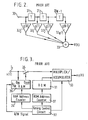
- Figs. 2 and 3 Conventional circuit arrangements for implementing the convolution algorithm are illustrated in Figs. 2 and 3 and have been described in a paper entitled "FIR Filter and Digital Signal Processing", Musen to Jikken, Special Edition, issued on November 20, 1979, pp.89-96.
- the circuit diagram shown in Fig. 2 is a basic arrangement for performing the convolution algorithm.
- input terminal 30 receives a digital data sequence x(t) consisting of a plurality of coded bytes (e.g., of 16 bits per byte) obtained through an analog-to-digital (A/D) conversion of an analog signal at sampling frequency w.
- A/D analog-to-digital
- the sequence x(t) is fed through a delay device 31 composed of N-1 delay elements 31 1 through 31 N-1 , each imparting a delay time T equal to the sampling period 1/F s .
- the outputs x(t) to x(t-N+l) of the delay elements 31 1 through 31 N-1 are sent to multipliers 32 0 through 32 N - 1 each having a corresponding filter coefficient g(i) (i-0, 1 , ..., N-1) derived from a desired impulse response or frequency transfer function.
- the outputs of the multipliers 32 0 through 32 N-1 are sent to an adder 33 to give a digital output sequence y(t).
- Such a structure achieves the required filtering characteristics given the appropriate coefficient factors g(i).
- the circuit shown in Fig. 2 requires a large number of delay elements and multipliers to implement a convolution algorithm of higher order.
- the circuit in Fig. 3 has been proposed in the previously mentioned November 1979 paper for improving the basic circuit shown in Fig. 2, and includes memories for storing an input data sequence x(t) and corresponding filter coefficients g(i).
- the set of coefficient data factors g(k) which are set beforehand, are stored in ROM (read-only memory) 31. These coefficient data factors g(k) are sequentially read from addresses provided by address counter 37 and the coefficient data are fed to multiplier/accumulator 33.
- the input signal x(t) which constitutes the other data sequence of the convolution arithmetic calculation, is supplied to input I from an external source at prescribed intervals.
- the input signal x(t) may be applied to multiplier/accumulator 33 through switch 35 or to a data input terminal D IN of RAM (random access memory) 36.
- Switch 35 determines whether input signal x(t) is fed to multiplier/accumulator 33 directly or is stored in RAM 36 for later presentation to the accumulator.
- the RAM 36 stores the input signal x(t) at certain prescribed times and is normally in a read mode so as to supply the stored input signals to multiplier/accumulator 33 through switch 35. Both the designation of the operating mode (read/write) and the application of addresses to RAM 36 (via RAM Address Counter 34) are carried out by timing control circuit 32 which is operated by a software-driven microcomputer.
- timing control circuit 32 also generates addresses for ROM 31 via ROM Address Counter 37 and further controls the operation mode of RAM 36 and the timing of multiplier/ accumulator 33.
- timing control circuit 32 and counters 34- and 37 indicate the addresses to enable sequential output of the coefficient data factors g(2), g(4), ..., g(2m) stored in ROM 31 and of the input signals x(t-l), x(t-2), ...x(t-m) stored in RAM 36 according to the proper correspondence between g(2k) x(t-k).
- a R/W (designating read/write) signal from the timing control circuit 32 is at the L (lov) level so RAM 36 is in the read mode.
- the R/W signal is also applied to a control terminal (not shown) of switch 35, so that the path of the input signal x(t) from the external source is disabled.
- the R/W signal changes to the H (high) level, putting RAM 36 into the write mode, and setting switch 35 to connect multiplier/accumulator 33 to the external source device so that the current input signal x(t) is fed both to multiplier/accumulator 33 and to RAM 36.
- Timing control circuit 32 simultaneously identifies the addresses of ROM 31 and RAM 36 so that the coefficient data factor g(k) corresponding to the input signal x(t) is read out from ROM 31 and the current input signal x(t) is stored at the prescribed address in RAM 36 ready for use in the next calculation.
- multiplier/accumulator 33 outputs the result of its convolution calculation in response to an output control signal from timing control circuit 32.
- the conventional convolution arithmetic circuit involves storing, in prescribed locations in the memory, two sets of data relating to the convolution calculation between the input signal x(t) and the coefficient data g(k), and supplying these sequentially to a multiplier/accumulator in accordance with a correspondence relationship, all these operations being controlled by a programmed microcomputer.
- the above conventional convolution arithmetic circuit has a certain flexibility in that it makes use of a programmable microcomputer, but, if it were to be applied as a digital filter in, for example, a DAD system, problems would arise regarding the processing speed of the microcomputer software rendering the convolution arithmetic circuit unable to cope with the data flow.
- One object of the invention is to provide a convolution arithmetic circuit suitable for real-time processing of digital signals.
- Another object of the invention is to provide a convolution arithmetic circuit having a simple construction for selecting different convolution formulae for data to be calculated.
- a convolution arithmetic circuit comprises: first memory means for storing a first data sequence; second memory means for storing a second data sequence determined from an input signal; first counter means providing cycles of count data, each said cycle including a sequence of non-repeated counts; second counter means providing a series of addresses for the second memory, multiplying/accumulating means for computing a series of products by multiplying elements of the first data sequence read from the first memory means by elements of the second data sequence read from the second memory means and for determining the sum of the products; and means for transforming each cycle of the count data into a series of addresses for the first memory means, each series of addresses including a sequence wherein at least one address is generated twice.
- a convolution arithmetic circuit includes first memory means for storing a first data sequence; second memory means for storing a second data sequence; third memory means for storing a third data sequence determined from an input signal; first counter means providing a series of first addresses for the first and second memory means; second counter means providing a series of second addresses for the third memory means; selection means for selectively supplying an output representing either the first or second data sequence read from the first or second memory in response to said first addresses; and multiplying/accumulating means for computing a series of products by multiplying elements of the third data sequence read from the third memory by the data sequence supplied by said selection means and for determining the sum of the products.
- Fig. 4 shows a circuit configuration of an embodiment of a convolution arithmetic circuit according to this invention.
- the sampling frequency of the coefficient data g(k) is set at a prescribed value as described hereinafter.
- the set of input terminals I gLSB to I gMSB of an accumulator 41 is connected to the set of output terminals O LSB to O MSB of a ROM 42 that stores the coefficient data factors g(k).
- ROM Address input terminals IA D0 to IA D3 of ROM 42 are connected to the output terminals of a system counter 44 through a ROM address altering circuit 43.
- - System counter 44 is a scale-of-24 counter including five D-type flip-flops (DFF) 44a l to 44a 5 coupled with each other by exclusive-OR (EX-OR) gates 44b 1 to 44b 4 , AND gates 44c 1 to 44c 3 and a NAND gate 44d.
- DFF D-type flip-flops
- EX-OR exclusive-OR
- Another set of input terminals I XLSB to I XMSB of accumulator 41, to which the multiplicand data are applied receive, with the prescribed timing (to be described subsequently), input signals x(t) (the data of each bit are xLSB to X MSB ) that are supplied from an external device through a gate 45 that has, arranged in parallel with it, a prescribed number of tri-state buffers 45a, corresponding to each bit. They are also connected to input/output (I/O) terminals I/O LSB to I/O MSB of a RAM 46, which holds a plurality of input signals constituting the multiplicand data.
- I/O input/output
- RAM address counter 47 is a "scale-of-six" counter and may be configured as the RAM address counter described in co-pending Europeans application 84308175.3.
- a control signal generating circuit 49 also described in that application is connected to output terminals Q0 to Q4 of system counter 44 for generating a R/W signal, a counter control signal Sc and an accumulator reset signal AR.
- the R/W signal specifies the operating mode of RAM 46 and is applied directly to a mode change terminal R/W of RAM 46 and to gate 45 through an inverter 48.
- the R/W signal when low (L), changes RAM 46 to a write-mode and permits the supply, to RAM 46 and multiplier/accumulator (M/A) 41, of the input signal x(t) that is then present at the input terminals of the tri-state buffer 45. While the R/W signal is high (H) RAM 46 is in read-mode and permits the supply, to M/A 41, of the signal stored in RAM 46. Gate 45 is disabled to prohibit the passage of the input signals x(t) to the input of M/A 41.
- the counter control signal Sc is applied to a control terminal of RAM address counter 47 and changes the count mode of RAM address counter 47 in response to the state of the counter control signal Sc.
- R AM address counter 47 performs an ordinary counter operation, i.e., incrementing the count by 1 with every CLOCK signal, while the counter control signal Sc is at level L. However, when the counter control signal Sc is at level H the count of RAM address counter 47 is incremented by +2 for each CLOCK signal.
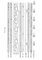
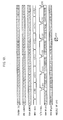
- counter 44- is a scale-of-24 counter it has a 24-count sequence as follows: 0, 3, 2, 5, 4, 7, 8, 11, 10, 13, 12, 15, 16, 19, 18, 21, 20, 23, 24, 27, 26, 29, 28, 31. This sequence automatically repeats itself as long as clock pulses are applied. This is represented in the SYSTEM COUNTER line of Fig. 6a.
- ROM address altering circuit 43 includes four EX-OR gates 43a 1 to 43a4 and an inverted EX-OR gate 43b.
- Inverted EX-OR gate 43b receives the output Q4 of system counter 44 and a select signal U/D.
- the control signal U/D is also applied to control signal generating circuit 49.
- EX-OR gate 43a4 also receives the output Q4 and receives as a second input the second most significant bit output Q3 of system counter 44.
- the rest of EX-OR gates 43a 1 to 43a 3 receive respectively the outputs Q0 to Q2 of system counter 44 as well as the output of inverted EX-OR gate 43b.
- Outputs AD 0 to AD 3 of EX-OR gates 43a 1 to 43a4 are respectively applied to input terminals IAD 0 to IAD 3 of ROM 42.
- EX-OR's 43a 1 -43a4 invert the Q0-Q3 outputs from counter 44.
- EX-OR 43b is "0” the QO-Q3 counter outputs are passed unchanged.
- the second twelve count states represented by the AD O -AD 3 signals are a "mirror image" of the first twelve AD O -AD 3 count states. This is illustrated in the "ROM ADDRESS" line of Fig. 6a.
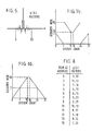
- ROM 42 stores twelve coefficient data factors g(k). However, twenty-four coefficient data factors are necessary for one convolution processing cycle in digital filtering. As shown in Fig. 5, the impulse response values 0-23 comprising the coefficient data factors present a symmetrical pattern such that each response in a symmetrical half is the same in amplitude as a corresponding one in the opposite symmetrical half. Accordingly, impulse response factors for one symmetrical half, in this case twelve impulse responses from the center of the symmetrical pattern, represent the coefficient data factors g(k) stored in ROM 42. The twenty-four coefficient data factors are stored at ROM addresses 0, 3, 2, 5, 4, 7, 8, 11, 10, 13, 12 and 15 as shown in Fig. 8.
- the outputs AD O to AD 3 of address altering circuit 43 respectively change as shown by signal waveforms AD 0 to AD 3 in Fig. 6a.
- the relationship of AD O -AD 3 to the count of system counter 44 is indicated by comparing the SYSTEM CTR line of Fig. 6a with AD O -AD 3 .
- the ROM addresses generated by the outputs AD O to AD 3 for ROM 42 change as shown in the ROM address line of Fig. 6a.
- the relationship between the ROM addresses and the count of system counter 44 is represented by the diagram shown in Fig. 6b.
- Each of the ROM addresses 0 to 15 is generated twice in a cycle of the system counter 44 from 0 to 31.
- the twelve coefficient data factors g(k) corresponding to the ROM addresses 0-15 are therefore read out and supplied to M/A 41 twice during one cycle of the count of system counter 44. First the coefficient data factors g(k) corresponding respectively to the ROM addresses 0 to 15 are read in turn for the count of 0 to 15 and then the coefficient data factors g(k) corresponding to the ROM ADDRESSES 15 to 0 are read in turn for the count of 16 to 31.
- the input signal x(t) is applied to input terminals Ix MSB to Ix LSB of MA 41 from the RAM 46 or from an external device through gate 45.
- the convolution operation for the coefficient data g(k) and the input signal x(t) at M/A 41 is performed under control of the R/W signal and the counter control signal Sc generated from control signal generating circuit 49.
- the convolution arithmetic circuit of Fig. 4 increases the effective sampling frequency by a factor of 4 by performing calculations defined by the following equations in response to an H level U/D signals
- the convolution operation is executed four times while the input signal x(t) is sampled once, thereby making the effective sampling frequency of the output data y(t) four times the sampling frequency of the input signal x(t).
- the variable (4t + ⁇ of the output y(4t + ⁇ ) (where - 0, 1, 2, 3) of the above equations is on the time domain, so the output data is, in fact, y'(4t + ⁇ ) with respect to the input data x(t), although the variable is expressed for convenience in integer form i.e., in the former form y(4t + ⁇ ).
- the output of RAM address counter 47 is applied to address terminals AD LSB to AD MSB of RAM 46 to change its address (RAM address) from 0, 1, ..., 5, 0, 1, ...5.
- the twelve data factors g(20), 9 (16), g(12), g(8), g(4) g(0), g(21), g(17), g(13), g(9), g(5), and g(l) (expressed as 20, 16, etc. in Fig. 6a) which are stored in ROM 42 at the ROM addresses 0, 3, 2, 5, 4, 7, 8, 11, 10, 13, 12, 15, respectively, are read out forward and backward sequentially.
- the multiplicand data x(0) to x(4), expressed by 0-4, respectively, in the RAM OUT line of Fig. 6a correspond to these coefficient data, and are stored in the RA M 46 at addresses 0 to 4 and are read out from RAM 46.
- Multiplier/accumulator (M/A) 41 sequentially calculates the products of these coefficient data and multiplicand data and keeps a running total of the products. M/A 41 thus calculates g(20) ⁇ x(0) + g(16) ⁇ x(1) + .... + g(4) ⁇ x(4), etc.
- the input signal x(5) is also supplied to M/A 41 in place of the output of RAM 46, and the input signal x(5) is multiplied by the coefficient data factor g(0) corresponding to the ROM address "7" and present at the ROM output. In this way, M/A 41 makes the final calculation for calculating the output data y(20) corresponding to the input signal x(5).
- the R/W signal changes to the H level and RAM 46 returns to the read-mode.
- the read-mode resumes until the count of system counter 44 becomes "8".
- the RAM addresses shift through 0, 1, ..., 5 under control of RAM address counter 47, causing the multiplicand data x(0), x(l), ...., x(5) corresponding to the RAM addresses to be read, the input signal x(5) in the preceding cycle having already been stored in the RAM address "5.”
- multiplier/accumulator 41 calculates g(21) ⁇ x(0) + g(17) ⁇ x(1) + ... + g(l).x(5).
- the count of system counter 44 is "15"
- the accumulating output is latched to hold the output data g(4j+l).x(5-j).
- the operation of the convolution circuit of Fig. 4 with the select signal U/D being at the L level is explained hereinafter with respect to the modified operation illustrated in Figs. 7a and 7b.
- the outputs AD 0 to AD 3 of address altering circuit 43 respectively change as shown in Fig. 7a according to the count illustrated in the SYSTEM CTR line.
- the ROM addresses produced by the outputs AD O to AD 3 change as shown in Fig. 7a at ROM Address.
- the relation of the ROM addresses with the count of system counter 44 is represented in the diagram of Fig. 7b.
- Each of the ROM addresses 0 to 15 is designated twice in a cycle of the count of system counter 44 from 0 to 31 similar to the cycle shown in Fig.
- the input signal x(t) is applied to input terminals Ix MSB to IX LSB of M/A 41 from RAM 46 or an external device through gate 45.
- the convolution operation for the coefficient data g(k) and the input signal x(t) at M/A 41 is performed under control of the R/W signal and the counter control signal Sc generated from RAM control circuit 49.
- the convolution arithmetic circuit of Fig. 4 decreases the effective sampling frequency by a factor of 1/4 when the select signal U/D is at the L level, performing calculations defined by the following equations:
- the convolution operation is executed one time while the input signal x(t) is sampled four times, thereby making the effective sampling frequency of the output data y(t) one-fourth of the sampling frequency of the input signal x(t).
- the variable (4t - 1). of the output data y(4t - 1) of the above equations is in the time domain, so the output data is, in fact, y( 4t - 1 ) with respect to the input data x(t), although the variable is expressed for convenience in integer form, i.e., in the former form y(4t - 1).
- accumulator 41 delivers its convolution output when the timing system counter 44 reaches a count of "31". That is, accumulator 41 delivers:
- Figs. 9-13 illustrate an alternate embodiment employing a different aspect of applicants' invention.
- the system shown in Fig. 9 employs a multiplier/accumulator 41, a RAM 46, RAM address counter 47, control signal generating circuit 49, and a system counter 44 identical to those same components shown and described above in connection with the Fig. 4 embodiment.
- the Fig. 9 system employs a pair of ROMs 42a and 42b. Further, the count conversion circuit 43 employed in the Fig. 4 system is not utilized and, instead, the five output lines QO-Q4 of scale-of-24 counter 44 are fed directly to the address inputs AD O -AD 4 of the ROMs 42a and 42b. Accordingly, the ROMs are simultaneously addressed with a continuous sequence of 5-bit address signals progressing in accordance with the normal counter sequence of scale-of-24 counter 44. Each address signal presented to the ROMs 42a, 42b reads out of the accessed storage location one of the filter coefficient data factors stored therein. The data factor values stored in the ROMs are the same as those depicted in connection with Fig.
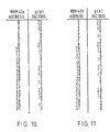
- Fig. 10 shows the storage locations of ROM 42a and the particular g(k) factor stored therein.
- Fig. 11 shows the storage locations of ROM 42b and the particular g(k) data factor stored therein.
- Selection signal U/D' shown in Fig. 9 operates a pair of gate circuits 43a and 43b to activate either the outputs from ROM 42a or the outputs from RO M s 42b, depending upon the state (H or L) of the U/D' signal.
- U/D' When U/D' is high, gates 43a are enabled such that the outputs from ROM 42a are fed to the inputs ILSB- I MSB of multiplier/accumulator 41 in response to the progression of system counter 44. Gates 43b are disabled and the outputs from ROM 42b are not utilized. However, when U/D' is at the L level, the opposite condition prevails and the outputs from ROM 42b are fed to the inputs I LSB -I MSB of multiplier/accumulator 41.
- the system operation achieved by the circuit of Fig. 9 is identical with the operation achieved in the circuit of Fig. 4 for the two states of the U/D signal.
- the F ig. 9 system performs digital filtering at the high sampling rate identically with the operation previously described in connection with Fig. 6a. While the operation depicted in Fig. 12 indicates that the ROM addresses sequence in sync with the outputs of the system counter, the outputs from the ROM 42a are exactly the same as the ROM outputs of the Fig. 4 system (Fig. 6a), whereupon the same filtering function and sampling rate operation are achieved.
Landscapes
- Engineering & Computer Science (AREA)
- Theoretical Computer Science (AREA)
- Computing Systems (AREA)
- Physics & Mathematics (AREA)
- General Physics & Mathematics (AREA)
- Computational Mathematics (AREA)
- Mathematical Physics (AREA)
- Computer Hardware Design (AREA)
- Mathematical Analysis (AREA)
- Mathematical Optimization (AREA)
- Pure & Applied Mathematics (AREA)
- General Engineering & Computer Science (AREA)
- Complex Calculations (AREA)
Applications Claiming Priority (6)
| Application Number | Priority Date | Filing Date | Title |
|---|---|---|---|
| JP59451/84 | 1984-03-29 | ||
| JP5945184A JPS60205670A (ja) | 1984-03-29 | 1984-03-29 | たたみ込み演算回路 |
| JP59452/84 | 1984-03-29 | ||
| JP59450/84 | 1984-03-29 | ||
| JP5945084A JPS60205669A (ja) | 1984-03-29 | 1984-03-29 | たたみ込み演算回路 |
| JP5945284A JPS60205671A (ja) | 1984-03-29 | 1984-03-29 | たたみ込み演算回路 |
Publications (3)
| Publication Number | Publication Date |
|---|---|
| EP0156648A2 true EP0156648A2 (fr) | 1985-10-02 |
| EP0156648A3 EP0156648A3 (en) | 1989-12-13 |
| EP0156648B1 EP0156648B1 (fr) | 1992-09-30 |
Family
ID=27296884
Family Applications (1)
| Application Number | Title | Priority Date | Filing Date |
|---|---|---|---|
| EP19850302161 Expired EP0156648B1 (fr) | 1984-03-29 | 1985-03-28 | Circuit arithmétique de convolution pour le traitement numérique de signaux |
Country Status (2)
| Country | Link |
|---|---|
| EP (1) | EP0156648B1 (fr) |
| DE (1) | DE3586692T2 (fr) |
Cited By (4)
| Publication number | Priority date | Publication date | Assignee | Title |
|---|---|---|---|---|
| GB2403360A (en) * | 2003-06-28 | 2004-12-29 | Zarlink Semiconductor Inc | Reduced complexity filter implementation |
| US8683182B2 (en) | 1995-08-16 | 2014-03-25 | Microunity Systems Engineering, Inc. | System and apparatus for group floating-point inflate and deflate operations |
| GB2555936A (en) * | 2016-10-27 | 2018-05-16 | Google Llc | Neural network compute tile |
| US10360163B2 (en) | 2016-10-27 | 2019-07-23 | Google Llc | Exploiting input data sparsity in neural network compute units |
Family Cites Families (2)
| Publication number | Priority date | Publication date | Assignee | Title |
|---|---|---|---|---|
| FR2417806A1 (fr) * | 1978-02-20 | 1979-09-14 | Dassault Electronique | Convoluteur numerique |
| DE3111889A1 (de) * | 1981-03-26 | 1982-10-14 | Philips Patentverwaltung | Digitales filter |
-
1985
- 1985-03-28 EP EP19850302161 patent/EP0156648B1/fr not_active Expired
- 1985-03-28 DE DE19853586692 patent/DE3586692T2/de not_active Expired - Fee Related
Cited By (12)
| Publication number | Priority date | Publication date | Assignee | Title |
|---|---|---|---|---|
| US8683182B2 (en) | 1995-08-16 | 2014-03-25 | Microunity Systems Engineering, Inc. | System and apparatus for group floating-point inflate and deflate operations |
| US8769248B2 (en) | 1995-08-16 | 2014-07-01 | Microunity Systems Engineering, Inc. | System and apparatus for group floating-point inflate and deflate operations |
| GB2403360A (en) * | 2003-06-28 | 2004-12-29 | Zarlink Semiconductor Inc | Reduced complexity filter implementation |
| GB2403360B (en) * | 2003-06-28 | 2006-07-26 | Zarlink Semiconductor Inc | Reduced complexity adaptive filter implementation |
| US7461113B2 (en) | 2003-06-28 | 2008-12-02 | Zarlink Semiconductor Inc. | Reduced complexity adaptive filter |
| GB2555936A (en) * | 2016-10-27 | 2018-05-16 | Google Llc | Neural network compute tile |
| GB2555936B (en) * | 2016-10-27 | 2019-01-30 | Google Llc | Neural network compute tile |
| US10360163B2 (en) | 2016-10-27 | 2019-07-23 | Google Llc | Exploiting input data sparsity in neural network compute units |
| US11106606B2 (en) | 2016-10-27 | 2021-08-31 | Google Llc | Exploiting input data sparsity in neural network compute units |
| US11422801B2 (en) | 2016-10-27 | 2022-08-23 | Google Llc | Neural network compute tile |
| US11816045B2 (en) | 2016-10-27 | 2023-11-14 | Google Llc | Exploiting input data sparsity in neural network compute units |
| US11816480B2 (en) | 2016-10-27 | 2023-11-14 | Google Llc | Neural network compute tile |
Also Published As
| Publication number | Publication date |
|---|---|
| DE3586692D1 (de) | 1992-11-05 |
| EP0156648B1 (fr) | 1992-09-30 |
| DE3586692T2 (de) | 1993-02-18 |
| EP0156648A3 (en) | 1989-12-13 |
Similar Documents
| Publication | Publication Date | Title |
|---|---|---|
| US4727505A (en) | Convolution arithmetic circuit for digital signal processing | |
| US4715257A (en) | Waveform generating device for electronic musical instruments | |
| US5103416A (en) | Programmable digital filter | |
| JPH0681011B2 (ja) | 可変通過帯域フイルタ装置 | |
| JPS6364100B2 (fr) | ||
| US4701875A (en) | High speed convolution arithmetic circuit with multiple counters | |
| US4866648A (en) | Digital filter | |
| EP0034241B1 (fr) | Filtre numérique non récursif | |
| JPH048965B2 (fr) | ||
| WO1991010955A1 (fr) | Processeur d'adresses pour processeur de signaux | |
| EP0156648B1 (fr) | Circuit arithmétique de convolution pour le traitement numérique de signaux | |
| US5189634A (en) | Digital signal processing apparatus for detecting a frequency component of digital signals | |
| US5381356A (en) | Cascade digital filters for realizing a transfer function obtained by cascade-connecting moving average filters | |
| EP0292189A2 (fr) | Mise à jour des coefficients de filtre canonique munis de digit de signe | |
| US5668746A (en) | Reproduced waveform equalization circuit | |
| US4586091A (en) | System and method for high density data recording | |
| JPS601939A (ja) | Pcm伝送システム | |
| EP0565358B1 (fr) | Filtre à phase linéaire avec inversion de la base de temps | |
| JPH0619797B2 (ja) | たたみ込み演算回路 | |
| US5130942A (en) | Digital filter with front stage division | |
| JPS6095599A (ja) | 時間軸圧縮伸張装置 | |
| JPS63103509A (ja) | デジタルフイルタ | |
| JPS61152115A (ja) | デジタルフイルタ | |
| JPH0795671B2 (ja) | デイジタルフイルタ | |
| JPH036691B2 (fr) |
Legal Events
| Date | Code | Title | Description |
|---|---|---|---|
| PUAI | Public reference made under article 153(3) epc to a published international application that has entered the european phase |
Free format text: ORIGINAL CODE: 0009012 |
|
| 17P | Request for examination filed |
Effective date: 19850415 |
|
| AK | Designated contracting states |
Designated state(s): DE FR GB NL |
|
| PUAL | Search report despatched |
Free format text: ORIGINAL CODE: 0009013 |
|
| AK | Designated contracting states |
Kind code of ref document: A3 Designated state(s): DE FR GB NL |
|
| RHK1 | Main classification (correction) |
Ipc: G06F 15/336 |
|
| 17Q | First examination report despatched |
Effective date: 19910521 |
|
| GRAA | (expected) grant |
Free format text: ORIGINAL CODE: 0009210 |
|
| AK | Designated contracting states |
Kind code of ref document: B1 Designated state(s): DE FR GB NL |
|
| REF | Corresponds to: |
Ref document number: 3586692 Country of ref document: DE Date of ref document: 19921105 |
|
| ET | Fr: translation filed | ||
| PLBE | No opposition filed within time limit |
Free format text: ORIGINAL CODE: 0009261 |
|
| STAA | Information on the status of an ep patent application or granted ep patent |
Free format text: STATUS: NO OPPOSITION FILED WITHIN TIME LIMIT |
|
| 26N | No opposition filed | ||
| PGFP | Annual fee paid to national office [announced via postgrant information from national office to epo] |
Ref country code: FR Payment date: 19960126 Year of fee payment: 12 |
|
| PGFP | Annual fee paid to national office [announced via postgrant information from national office to epo] |
Ref country code: GB Payment date: 19960319 Year of fee payment: 12 |
|
| PGFP | Annual fee paid to national office [announced via postgrant information from national office to epo] |
Ref country code: DE Payment date: 19960326 Year of fee payment: 12 |
|
| PGFP | Annual fee paid to national office [announced via postgrant information from national office to epo] |
Ref country code: NL Payment date: 19960328 Year of fee payment: 12 |
|
| PG25 | Lapsed in a contracting state [announced via postgrant information from national office to epo] |
Ref country code: GB Effective date: 19970328 |
|
| PG25 | Lapsed in a contracting state [announced via postgrant information from national office to epo] |
Ref country code: NL Effective date: 19971001 |
|
| GBPC | Gb: european patent ceased through non-payment of renewal fee |
Effective date: 19970328 |
|
| PG25 | Lapsed in a contracting state [announced via postgrant information from national office to epo] |
Ref country code: FR Free format text: LAPSE BECAUSE OF NON-PAYMENT OF DUE FEES Effective date: 19971128 |
|
| NLV4 | Nl: lapsed or anulled due to non-payment of the annual fee |
Effective date: 19971001 |
|
| PG25 | Lapsed in a contracting state [announced via postgrant information from national office to epo] |
Ref country code: DE Effective date: 19971202 |
|
| REG | Reference to a national code |
Ref country code: FR Ref legal event code: ST |