EP0156683A1 - Gerät für optische Microlithografie mit lokalem Ausrichtungssystem - Google Patents
Gerät für optische Microlithografie mit lokalem Ausrichtungssystem Download PDFInfo
- Publication number
- EP0156683A1 EP0156683A1 EP85400335A EP85400335A EP0156683A1 EP 0156683 A1 EP0156683 A1 EP 0156683A1 EP 85400335 A EP85400335 A EP 85400335A EP 85400335 A EP85400335 A EP 85400335A EP 0156683 A1 EP0156683 A1 EP 0156683A1
- Authority
- EP
- European Patent Office
- Prior art keywords
- wafer
- alignment
- objective
- image
- optical
- Prior art date
- Legal status (The legal status is an assumption and is not a legal conclusion. Google has not performed a legal analysis and makes no representation as to the accuracy of the status listed.)
- Granted
Links
- 230000003287 optical effect Effects 0.000 title claims description 38
- 238000001393 microlithography Methods 0.000 title claims description 25
- 238000007540 photo-reduction reaction Methods 0.000 claims abstract description 21
- 238000005286 illumination Methods 0.000 claims description 10
- 238000006073 displacement reaction Methods 0.000 claims description 9
- 230000005855 radiation Effects 0.000 claims description 3
- 238000004519 manufacturing process Methods 0.000 abstract description 7
- 238000000034 method Methods 0.000 description 17
- 230000004075 alteration Effects 0.000 description 3
- 238000005530 etching Methods 0.000 description 3
- 239000011521 glass Substances 0.000 description 3
- 239000011347 resin Substances 0.000 description 3
- 229920005989 resin Polymers 0.000 description 3
- 239000004020 conductor Substances 0.000 description 1
- 230000007547 defect Effects 0.000 description 1
- 230000008021 deposition Effects 0.000 description 1
- 238000010894 electron beam technology Methods 0.000 description 1
- 239000002184 metal Substances 0.000 description 1
Images

Classifications
-
- G—PHYSICS
- G03—PHOTOGRAPHY; CINEMATOGRAPHY; ANALOGOUS TECHNIQUES USING WAVES OTHER THAN OPTICAL WAVES; ELECTROGRAPHY; HOLOGRAPHY
- G03F—PHOTOMECHANICAL PRODUCTION OF TEXTURED OR PATTERNED SURFACES, e.g. FOR PRINTING, FOR PROCESSING OF SEMICONDUCTOR DEVICES; MATERIALS THEREFOR; ORIGINALS THEREFOR; APPARATUS SPECIALLY ADAPTED THEREFOR
- G03F9/00—Registration or positioning of originals, masks, frames, photographic sheets or textured or patterned surfaces, e.g. automatically
- G03F9/70—Registration or positioning of originals, masks, frames, photographic sheets or textured or patterned surfaces, e.g. automatically for microlithography
Definitions
- the present invention relates to an optical microlithography apparatus used in particular for the manufacture of integrated circuits. It relates more particularly to the local alignment system.
- an integrated circuit is manufactured by a succession of layer deposits and etching of these layers.
- the integrated circuit is covered with a layer of photosensitive resin and this resin is exposed with an energy beam which is intercepted by a mask reproducing the image of the pattern to be produced on the integrated circuit.
- the insolated resin is then removed leaving bare the areas of the integrated circuit to be etched.
- the most common method consists in making a mask with the 'scale 1.
- This method called 1: 1 projection, is interesting for its low cost and for its simplicity which allows high speed production.
- the apparatus of the invention is based on the first method. More particularly, it implements the method of direct photorepetition on edge (in English "direct step on wafer”). In this method the ratio of the respective dimensions of a mask and an integrated circuit is of the order of 10 to 1; a photoreduction objective is therefore placed between them.
- the device comprises means for moving the wafer.
- This means performs a displacement of the wafer of a constant pitch between two exposures.
- the length of the displacement can be controlled, for example, by a method employing laser beam interference.
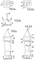
- Two known methods are used to align the integrated circuits of a wafer in the optical axis of the device. These two methods will be described with reference to FIGS. 1 and 2. These methods are respectively the global alignment method and the local alignment method.
- FIG. 1a shows, in top view, a plate 2 comprising a plurality of rectangular zones 4 regularly arranged on this plate. On these zones, successive layers will be deposited then engraved thus creating an integrated circuit. These zones will be called “bullets" in the remainder of the text.
- the wafer 2 also includes marking marks 6 which are used to align said wafer. These marks may consist of a single line, as shown in the figure, or may be two-dimensional, for example a cross. In the first case at least two marks are necessary to position the wafer in translation and in rotation; in the second case, one brand is sufficient.
- the alignment of the wafer is achieved by an optical system shown diagrammatically in FIG.
- the optical system shown comprises two angle mirrors 8, a prism 10 and an alignment microscope 12. This optical system is connected to a means which controls the movement of the support of the wafer so that the registration marks 6 occupy reference positions.
- the plate is then translated to be positioned under the optical column of the microlithography system.
- This optical system comprises a source S of monochromatic light, a converging lens 14, a reticle 16, consisting of a glass slide 18 on the underside of which a mask 20 is produced by deposition and then etching of a metal sheet, and a photoreduction objective 22.
- a source S of monochromatic light a converging lens 14
- a reticle 16 consisting of a glass slide 18 on the underside of which a mask 20 is produced by deposition and then etching of a metal sheet
- a photoreduction objective 22 for a photoreduction objective 22.
- Each chip 4 of the wafer 2 is successively exposed.
- FIG. 2a represents a top view of a wafer 2 comprising a plurality of chips 4.
- a locating mark 24 is placed next to each of the chips. These marks allow each chip to be individually aligned under the optical microlithography system. These marks can be one-dimensional, for example a line, or two-dimensional, for example a cross.
- the optical microlithography system of FIG. 2b comprises the same elements as that of FIG. 1c, that is to say a monochromatic source S, a converging lens 14, a reticle 16 consisting of a glass slide 18 and d 'a mask 20 and a photoreduction objective 22.
- a reference mark 26 has been added on the blade 18 next to the mask 20. This mark is projected by the photoreduction objective 22 on the wafer 2. The correct alignment of a chip in the wafer is achieved by coinciding the projection of this mark 26 with the marking mark 24 of the chip located under the photoreduction objective. The image of the mark 26 on the wafer 2 and the surrounding area is returned by a beam splitter 28 disposed between the reticle 16 and the photoreduction objective 22 to be analyzed. A displacement means then controls the movement of the wafer as a function of this signal 29 in order to correctly align the chip 4 to be exposed.
- Local alignment allows better precision in the superposition of the different layers of a chip.
- the alignment accuracy here is 0.1 ⁇ m , which is significantly better than in devices with a global alignment system. It is thus possible to produce integrated circuits whose minimum dimension of the patterns is of the order of 1 ⁇ m.
- each chip penalizes the production rate of the integrated circuits with respect to the overall alignment.
- the realignment is not carried out all the chips, but all the n chips, the value of n being chosen as a function of the characteristics of the device.
- the local alignment system of the apparatus shown in Figure 2b is not perfect.
- a first limitation of this system lies in the fact that the photoreduction objective 22 is only corrected for a precise wavelength which is the wavelength of the monochromatic source S. Correct alignment cannot therefore be done than with this source. This is inconvenient because the locating mark 24 located in the field of the photoreduction objective 22 is attacked by the radiation coming from the source S.
- the locating mark 24 may have very little contrast, which makes it difficult to align the associated chip 4.
- the local alignment system of the apparatus of the invention overcomes these problems by authorizing the illumination of mark 24 by a broad spectrum optical beam or by the choice of a monochromatic beam whose wavelength can be chosen from a plurality.
- a broad spectrum optical beam or by the choice of a monochromatic beam whose wavelength can be chosen from a plurality.
- the photoreduction objective which is devoid of aberrations for a single wavelength, is not compatible with the illumination source of the invention. Furthermore, a photoreduction objective devoid of aberrations for a range of wavelengths is practically impossible to achieve in the current state of the art.
- This beam splitter also has the role of returning the image of the area surrounding the identification mark of the chip to be exposed, an image which is then processed by a means which controls the movement of the wafer to achieve alignment of the chip. to be exposed.
- the invention relates to an optical microlithography device comprising a support receiving a wafer on which are distributed chips to be exposed each provided with at least one locating mark in position, an optical system, and a system of alignment of the wafer, said optical system comprising a radiation source, a converging lens, a reticle and a photoreduction objective for displaying the image of the reticle on a chip of the wafer, said local alignment system comprising a separator of beam between the photoreduction objective and the wafer, a source of illumination of the wafer by said beam splitter, means for collecting by said beam splitter the image of the illuminated area around the registration mark, a alignment pattern and a means for control the movement of the insert holder to align the image of the registration mark with the alignment pattern.
- the photoreduction objective is not used by the alignment system.
- the light from the illumination source is transmitted and deflected only by the beam splitter, and the image of the chip collected after reflection of this light is transmitted and deflected only by said beam splitter.
- the light source can be either broad spectrum or monochromatic.
- a monochromatic source can in particular be obtained by interposing a filter on the path of a broad spectrum beam.
- the alignment system comprises two alignment patterns and two means for collecting the image of two registration marks associated with a chip, the displacement means moving the wafer to align each registration mark. marking with an alignment pattern.
- each means for collecting the image of the registration mark is an aiming objective having in its focal plane the alignment pattern.
- the optical microlithography system of the apparatus shown in Figure 3 is conventional. It comprises a monochromatic source S, a converging lens 14, a reticle 16 composed of a glass slide 18 on the underside of which is engraved a mask 20, and a photoreduction objective 22.
- a displacement means (not shown) successively positions each chip 4 of the wafer 2 in the axis of the optical microlithography system to expose them.
- the local alignment system of the optical microlithography apparatus comprises a beam splitter 30 disposed in the axis of the optical system between the photoreduction objective 22 and the wafer 2, an aiming objective 32 for collect the image of the area of the wafer centered on the locating mark 24 associated with the chip 4 to be exposed, a light source S ', a second beam splitter 34 and an alignment pattern 36.
- the beam splitter 30 can in particular be a separator cube or a dichroic mirror. This beam splitter 30 forms, with the photoreductive objective 22 a whole, optically and mechanically inseparable.
- the beam splitter 30 can also consist of a retractable mirror. In this case, it may be necessary to move the mirror to allow sunshine. The chip insolation flow is then less important.
- the lens 14, the photoreduction objective 22 and the beam splitter 30 are aligned on the optical axis of the device. They are fixed relative to this axis.
- the alignment of the reticle is obtained, in a known manner, by placing registration marks on this reticle in coincidence with registration marks on the reticle holder (not shown).
- the wafer 2 is illuminated by the source S 'of the local alignment system, the beam from the source S being obscured.
- the viewing objective 32 has two degrees of freedom in translation in the plane perpendicular to the axis of the optical microlithography system. It is moved in a known manner, either manually or automatically, so that the registration mark 24 associated with the chip 4 falls within its field of vision.
- the alignment pattern 36 follows the movements of the aiming objective, for example by being integral with this aiming objective by means of a frame 33, in order to be maintained in the focal plane 35 of the objective. aiming device 32. Additional optical means, not shown, such as angle references, allow the beam coming from the source S 'to illuminate the wafer 2 by means of the beam splitter 34 and objective 32 regardless of the position of the latter.
- the alignment of the chip 4 is achieved by comparing the position of the alignment pattern 36 and the image of the registration mark 24 in the focal plane of the aiming objective 32.
- a means controls the displacement of the plate to corner these two marks.
- the comparison of the position of the alignment pattern and the image of the registration mark can be carried out according to any known method. It may in particular be a photometric method if the registration mark and the alignment pattern are respectively a male cross and a female cross, or it may be a correlation method if the registration mark and the alignment pattern each form a network.
- the light source S ′ can be monochromatic or broad spectrum.
- the light source can thus be chosen according to the technological level in order to always have a very contrasted marking mark 24.
- a simple embodiment of this versatile illumination source S ′ consists in using a broad spectrum source S ′, for example of wavelength between 300 and 800 nanometers, and a set of removable filters intercepting the beam of the source SI. These filters can, for example, be distributed over the periphery of a disc, the rotation of which makes it possible to present any filter in front of the source S '.
- the local alignment system of the device shown in FIG. 3 makes it possible to align the wafer 2 in translation, the alignment in rotation being carried out once and for all at the start of the sunshine.
- Alignment in rotation and in position can also be achieved if each chip 4 of the wafer 2 is associated with two registration marks and if the local alignment system includes two aiming objectives to project the image of each of these marks on alignment patterns.
- FIG. 4 schematically illustrates such an alignment system. This figure shows the lower part of the optical microlithography system comprising the photoreduction objective 22 and the beam splitter 30.
- Each chip 4 of the wafer 2 is provided with two reference marks 24a and 24b.
- the light source (not shown) illuminates the zones located around the registration marks 24a and 24b and returns the image of these zones on the plane 38, located in the focal plane of the viewing objectives 32a and 32b, on which are inscribed two alignment patterns 36a and 36b.
- the alignment can be carried out all the chips or only all the n chips, where n is an integer greater than or equal to 1.
Landscapes
- Physics & Mathematics (AREA)
- General Physics & Mathematics (AREA)
- Exposure And Positioning Against Photoresist Photosensitive Materials (AREA)
- Exposure Of Semiconductors, Excluding Electron Or Ion Beam Exposure (AREA)
Applications Claiming Priority (2)
| Application Number | Priority Date | Filing Date | Title |
|---|---|---|---|
| FR8403027 | 1984-02-28 | ||
| FR8403027A FR2560397B1 (fr) | 1984-02-28 | 1984-02-28 | Appareil de microlithographie optique a systeme d'alignement local |
Publications (2)
| Publication Number | Publication Date |
|---|---|
| EP0156683A1 true EP0156683A1 (de) | 1985-10-02 |
| EP0156683B1 EP0156683B1 (de) | 1989-11-08 |
Family
ID=9301472
Family Applications (1)
| Application Number | Title | Priority Date | Filing Date |
|---|---|---|---|
| EP85400335A Expired EP0156683B1 (de) | 1984-02-28 | 1985-02-22 | Gerät für optische Microlithografie mit lokalem Ausrichtungssystem |
Country Status (5)
| Country | Link |
|---|---|
| US (1) | US4685807A (de) |
| EP (1) | EP0156683B1 (de) |
| JP (1) | JPS60205453A (de) |
| DE (1) | DE3574187D1 (de) |
| FR (1) | FR2560397B1 (de) |
Families Citing this family (12)
| Publication number | Priority date | Publication date | Assignee | Title |
|---|---|---|---|---|
| US4795244A (en) * | 1985-09-20 | 1989-01-03 | Nikon Corporation | Projection type exposure apparatus |
| US5148214A (en) * | 1986-05-09 | 1992-09-15 | Canon Kabushiki Kaisha | Alignment and exposure apparatus |
| US5137363A (en) * | 1986-06-04 | 1992-08-11 | Canon Kabushiki Kaisha | Projection exposure apparatus |
| US4782368A (en) * | 1986-07-11 | 1988-11-01 | Matsushita Electric Industrial, Co., Ltd. | Method for correction for chromatic aberration and exposure apparatus using the same |
| US5317338A (en) * | 1991-10-29 | 1994-05-31 | International Business Machines Corporation | Visual measurement technique and test pattern for aperture offsets in photoplotters |
| US5233460A (en) * | 1992-01-31 | 1993-08-03 | Regents Of The University Of California | Method and means for reducing speckle in coherent laser pulses |
| US5519535A (en) * | 1994-04-04 | 1996-05-21 | Motorola, Inc. | Precision placement apparatus having liquid crystal shuttered dual prism probe |
| US5943089A (en) * | 1996-08-23 | 1999-08-24 | Speedline Technologies, Inc. | Method and apparatus for viewing an object and for viewing a device that acts upon the object |
| JPH1199704A (ja) * | 1997-09-30 | 1999-04-13 | Noritsu Koki Co Ltd | 印画紙用カラープリントヘッド |
| JP4157204B2 (ja) * | 1998-10-19 | 2008-10-01 | セイコーインスツル株式会社 | 情報再生装置、情報記録装置、情報再生方法および情報記録方法 |
| US7870891B2 (en) * | 2004-05-29 | 2011-01-18 | Kilr-Chilr, Llc | Systems, devices and methods for regulating temperatures of tanks, containers and contents therein |
| CN102944978B (zh) * | 2011-08-15 | 2014-08-06 | 中山新诺科技股份有限公司 | 曝光系统、校准系统、光学引擎、曝光方法和制造方法 |
Citations (5)
| Publication number | Priority date | Publication date | Assignee | Title |
|---|---|---|---|---|
| DE1597431A1 (de) * | 1967-09-30 | 1970-04-23 | Telefunken Patent | Verfahren zur Herstellung von Mikrostrukturen auf einem Substrat |
| FR2082213A5 (de) * | 1970-03-06 | 1971-12-10 | Delmas Jean Raymond | |
| FR2128822A1 (de) * | 1971-03-11 | 1972-10-20 | Asahi Optical Co Ltd | |
| US3718396A (en) * | 1971-12-28 | 1973-02-27 | Licentia Gmbh | System for photographic production of semiconductor micro structures |
| US3844655A (en) * | 1973-07-27 | 1974-10-29 | Kasper Instruments | Method and means for forming an aligned mask that does not include alignment marks employed in aligning the mask |
Family Cites Families (2)
| Publication number | Priority date | Publication date | Assignee | Title |
|---|---|---|---|---|
| US4385838A (en) * | 1980-01-19 | 1983-05-31 | Nippon Kogaku K. K. | Alignment device |
| US4419013A (en) * | 1981-03-30 | 1983-12-06 | Tre Semiconductor Equipment Corporation | Phase contrast alignment system for a semiconductor manufacturing apparatus |
-
1984
- 1984-02-28 FR FR8403027A patent/FR2560397B1/fr not_active Expired
-
1985
- 1985-02-15 US US06/702,393 patent/US4685807A/en not_active Expired - Fee Related
- 1985-02-22 EP EP85400335A patent/EP0156683B1/de not_active Expired
- 1985-02-22 DE DE8585400335T patent/DE3574187D1/de not_active Expired
- 1985-02-25 JP JP60034679A patent/JPS60205453A/ja active Pending
Patent Citations (5)
| Publication number | Priority date | Publication date | Assignee | Title |
|---|---|---|---|---|
| DE1597431A1 (de) * | 1967-09-30 | 1970-04-23 | Telefunken Patent | Verfahren zur Herstellung von Mikrostrukturen auf einem Substrat |
| FR2082213A5 (de) * | 1970-03-06 | 1971-12-10 | Delmas Jean Raymond | |
| FR2128822A1 (de) * | 1971-03-11 | 1972-10-20 | Asahi Optical Co Ltd | |
| US3718396A (en) * | 1971-12-28 | 1973-02-27 | Licentia Gmbh | System for photographic production of semiconductor micro structures |
| US3844655A (en) * | 1973-07-27 | 1974-10-29 | Kasper Instruments | Method and means for forming an aligned mask that does not include alignment marks employed in aligning the mask |
Also Published As
| Publication number | Publication date |
|---|---|
| FR2560397A1 (fr) | 1985-08-30 |
| FR2560397B1 (fr) | 1986-11-14 |
| JPS60205453A (ja) | 1985-10-17 |
| DE3574187D1 (en) | 1989-12-14 |
| US4685807A (en) | 1987-08-11 |
| EP0156683B1 (de) | 1989-11-08 |
Similar Documents
| Publication | Publication Date | Title |
|---|---|---|
| EP0015173B1 (de) | Optisches Ausrichtsystem für zwei Patronen und Photorepetierer mit solchem System | |
| EP0113633B1 (de) | Verfahren und Vorrichtung zur optischen Ausrichtung von Motiven in nahe zueinander liegenden Flächen, in einem Belichtungsgerät mit einer divergierenden strahlenden Lichtquelle | |
| FR2482285A1 (fr) | Procede et dispositif d'alignement d'un masque et d'une tranche notamment pour la fabrication de circuits integres | |
| EP0030899B1 (de) | Optische Ausrichtvorrichtung für zwei Motive mit gitterartigen Ausrichtmarken, insbesondere für die direkte Photowiedergabe auf Silizium | |
| EP0063980B1 (de) | Projektionsapparat mit einer Anordnung zum Scharfeinstellen | |
| EP0401351B1 (de) | Verfahren und vorrichtung für optische messungen | |
| EP0010998B1 (de) | Verfahren zum optischen Ausrichten von Motiven in zwei naheliegenden Flächen und Alignierungsvorrichtung zur Ausführung eines solchen Verfahrens | |
| EP0156683B1 (de) | Gerät für optische Microlithografie mit lokalem Ausrichtungssystem | |
| EP3077873B1 (de) | Vorrichtung und verfahren zur positionierung einer fotolithografischen maske mittels eines berührungslosen optischen verfahrens | |
| FR2504288A1 (fr) | Procede et appareil d'alignement d'une tranche de semi-conducteur | |
| EP0015789B1 (de) | Optische photorepetierende Projektionsvorrichtung | |
| EP0030878B1 (de) | Optische Ausrichtvorrichtung für zwei Motive und Photorepetierer mit einer solchen Vorrichtung | |
| FR2536873A1 (fr) | Appareil et procede d'exposition | |
| FR2541471A1 (fr) | Element en forme de feuille a aligner sur un autre element presentant une zone dessinee, et appareil et reticule pour l'alignement de ces elements | |
| FR2950155A1 (fr) | Procede d'alignement pour controler un miroir | |
| WO2000057235A2 (en) | Multi-beam scanner including a dove prism array | |
| EP0088691B1 (de) | Justiereinrichtung bei Maschinen zum Herstellen integrierter Schaltungen | |
| WO2021019136A1 (fr) | Dispositif d'inspection d'une surface d'un objet | |
| WO2007028793A1 (fr) | Illuminateur d'un dispositif de photolithographie | |
| FR2518255A1 (fr) | Appareil d'alignement precis de plaquettes semi-conductrices | |
| EP1880249B1 (de) | Optisches system für eine lithographievorrichtung | |
| EP0194231B1 (de) | Vorrichtung zur Belichtung diskreter Teile einer photoempfindlichen Oberfläche mittels eines Lichtstrahls | |
| EP0083268A1 (de) | Verfahren zur automatischen Regelung der Schärfe von auf einen Schirm projizierten Bildern und Geräte dazu | |
| JPH11287616A (ja) | 2光束生成装置及び位置検出装置 | |
| FR2791431A1 (fr) | Dispositif optique de reglage en distorsion d'un appareil a optique afocale |
Legal Events
| Date | Code | Title | Description |
|---|---|---|---|
| PUAI | Public reference made under article 153(3) epc to a published international application that has entered the european phase |
Free format text: ORIGINAL CODE: 0009012 |
|
| AK | Designated contracting states |
Designated state(s): CH DE GB LI NL |
|
| 17P | Request for examination filed |
Effective date: 19860308 |
|
| 17Q | First examination report despatched |
Effective date: 19870309 |
|
| RAP1 | Party data changed (applicant data changed or rights of an application transferred) |
Owner name: COMMISSARIAT A L'ENERGIE ATOMIQUE |
|
| GRAA | (expected) grant |
Free format text: ORIGINAL CODE: 0009210 |
|
| AK | Designated contracting states |
Kind code of ref document: B1 Designated state(s): CH DE GB LI NL |
|
| REF | Corresponds to: |
Ref document number: 3574187 Country of ref document: DE Date of ref document: 19891214 |
|
| GBT | Gb: translation of ep patent filed (gb section 77(6)(a)/1977) | ||
| PLBE | No opposition filed within time limit |
Free format text: ORIGINAL CODE: 0009261 |
|
| STAA | Information on the status of an ep patent application or granted ep patent |
Free format text: STATUS: NO OPPOSITION FILED WITHIN TIME LIMIT |
|
| 26N | No opposition filed | ||
| PGFP | Annual fee paid to national office [announced via postgrant information from national office to epo] |
Ref country code: DE Payment date: 19910124 Year of fee payment: 7 |
|
| PGFP | Annual fee paid to national office [announced via postgrant information from national office to epo] |
Ref country code: CH Payment date: 19910213 Year of fee payment: 7 |
|
| PGFP | Annual fee paid to national office [announced via postgrant information from national office to epo] |
Ref country code: GB Payment date: 19910221 Year of fee payment: 7 |
|
| PGFP | Annual fee paid to national office [announced via postgrant information from national office to epo] |
Ref country code: NL Payment date: 19910228 Year of fee payment: 7 |
|
| PG25 | Lapsed in a contracting state [announced via postgrant information from national office to epo] |
Ref country code: GB Effective date: 19920222 |
|
| PG25 | Lapsed in a contracting state [announced via postgrant information from national office to epo] |
Ref country code: LI Effective date: 19920229 Ref country code: CH Effective date: 19920229 |
|
| PG25 | Lapsed in a contracting state [announced via postgrant information from national office to epo] |
Ref country code: NL Effective date: 19920901 |
|
| NLV4 | Nl: lapsed or anulled due to non-payment of the annual fee | ||
| GBPC | Gb: european patent ceased through non-payment of renewal fee | ||
| REG | Reference to a national code |
Ref country code: CH Ref legal event code: PL |
|
| PG25 | Lapsed in a contracting state [announced via postgrant information from national office to epo] |
Ref country code: DE Effective date: 19921103 |