EP0157555A2 - Laser à semi-conducteur et procédé pour sa fabrication - Google Patents
Laser à semi-conducteur et procédé pour sa fabrication Download PDFInfo
- Publication number
- EP0157555A2 EP0157555A2 EP85301989A EP85301989A EP0157555A2 EP 0157555 A2 EP0157555 A2 EP 0157555A2 EP 85301989 A EP85301989 A EP 85301989A EP 85301989 A EP85301989 A EP 85301989A EP 0157555 A2 EP0157555 A2 EP 0157555A2
- Authority
- EP
- European Patent Office
- Prior art keywords
- substrate
- projection
- stripe
- multilayered
- group
- Prior art date
- Legal status (The legal status is an assumption and is not a legal conclusion. Google has not performed a legal analysis and makes no representation as to the accuracy of the status listed.)
- Granted
Links
Images


Classifications
-
- H—ELECTRICITY
- H01—ELECTRIC ELEMENTS
- H01S—DEVICES USING THE PROCESS OF LIGHT AMPLIFICATION BY STIMULATED EMISSION OF RADIATION [LASER] TO AMPLIFY OR GENERATE LIGHT; DEVICES USING STIMULATED EMISSION OF ELECTROMAGNETIC RADIATION IN WAVE RANGES OTHER THAN OPTICAL
- H01S5/00—Semiconductor lasers
- H01S5/20—Structure or shape of the semiconductor body to guide the optical wave ; Confining structures perpendicular to the optical axis, e.g. index or gain guiding, stripe geometry, broad area lasers, gain tailoring, transverse or lateral reflectors, special cladding structures, MQW barrier reflection layers
- H01S5/22—Structure or shape of the semiconductor body to guide the optical wave ; Confining structures perpendicular to the optical axis, e.g. index or gain guiding, stripe geometry, broad area lasers, gain tailoring, transverse or lateral reflectors, special cladding structures, MQW barrier reflection layers having a ridge or stripe structure
- H01S5/227—Buried mesa structure ; Striped active layer
-
- Y—GENERAL TAGGING OF NEW TECHNOLOGICAL DEVELOPMENTS; GENERAL TAGGING OF CROSS-SECTIONAL TECHNOLOGIES SPANNING OVER SEVERAL SECTIONS OF THE IPC; TECHNICAL SUBJECTS COVERED BY FORMER USPC CROSS-REFERENCE ART COLLECTIONS [XRACs] AND DIGESTS
- Y10—TECHNICAL SUBJECTS COVERED BY FORMER USPC
- Y10S—TECHNICAL SUBJECTS COVERED BY FORMER USPC CROSS-REFERENCE ART COLLECTIONS [XRACs] AND DIGESTS
- Y10S148/00—Metal treatment
- Y10S148/095—Laser devices
-
- Y—GENERAL TAGGING OF NEW TECHNOLOGICAL DEVELOPMENTS; GENERAL TAGGING OF CROSS-SECTIONAL TECHNOLOGIES SPANNING OVER SEVERAL SECTIONS OF THE IPC; TECHNICAL SUBJECTS COVERED BY FORMER USPC CROSS-REFERENCE ART COLLECTIONS [XRACs] AND DIGESTS
- Y10—TECHNICAL SUBJECTS COVERED BY FORMER USPC
- Y10S—TECHNICAL SUBJECTS COVERED BY FORMER USPC CROSS-REFERENCE ART COLLECTIONS [XRACs] AND DIGESTS
- Y10S148/00—Metal treatment
- Y10S148/11—Metal-organic CVD, ruehrwein type
Definitions
- This invention relates to a semiconductor laser and a method of producing the same which has recently rapidly extended its application to light sources for various types of electronic equipment and optical apparatus and is now greatly demanded.
- One of the important performances of a semiconductor laser which are demanded for the coherent light source of electronic equipment or optical apparatus is the oscillation at a single spot, or single transversal mode oscillation. To realize this, it is necessary to suppress the spread of laser light and confine the light by concentration current flowing through the laser element near the active region in which the laser light propagates.
- This type of semiconductor laser is normally called the stripe- type semiconductor laser.
- a relatively simple method for the stripe type is to only restrict current to be narrow.
- the laser according to this method needs a high threshold value for realization of the single transversal mode oscillation.
- the stripe type which can oscillate at the lowest threshold is a buried stripe type semiconductor laser (normally called the BH laser).
- the production of this type of laser requires to perform twice the crystal growth process which the other lasers need normally once, that is, it is necessary that after the multilayered films including an active layer are grown, the buried region be removed and then a buried layer be again grown. In addition, it is somewhat technically difficult to produce this laser.
- a method of producing a semiconductor laser comprising the steps of forming multilayered thin films of double heterostructure including an active layer on a semiconductor substrate having a stripe-shaped projection by the metal organic chemical vapor phase epitaxial growth method or molecular beam epitaxial growth method, and doping an impurity material of a conductivity type opposite to that of the semiconductor substrate into the top layer of the multilayered thin films formed on the stripe-shaped projection.
- an n-type GaAs substrate is used for a conductive substrate.
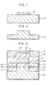
- a photoresist layer 16 with a width d is formed on the (100) plane of an n-type GaAs substrate 10 as shown in Fig. 1, and this substrate 10 is chemically etched to have recesses and a projection in parallel with the direction ⁇ 011> except the area masked by the photoresist layer 16, in order to have a stripe-shaped projection 5 ⁇ m wide and 1.5 ⁇ m high as shown in Fig. 2.
- an n-type Ga 1-x Al x As clad layer 11, 1.5 ⁇ m thick; an undoped Ga 1-y Al y As (0 ⁇ y ⁇ x) active layer 12, 0.08 ⁇ m thick; a p-type Ga 1-x Al x As clad layer 13, 1.2 ⁇ m thick; and then an n-type GaAs cap layer 14, 2 ⁇ m thick are sequentially grown over the substrate by the metal organic chemical vapor deposition method (normally, MOCVD method).
- the conditions for the crystal growth are, for example, as follows: the growth rate is 2 ⁇ m/hour; the growth temperature is 770°C; the flow rate of all gases is 5 l/min.; and the mol ratio of V group element to III-group element is 40.
- the epitaxial growth of up to the p-type Ga 1-x Al x As clad layer 13 on the projection of the substrate is made independently of that on the other areas, that is, the epitaxial growth of the materials is accompanied by no effect of diffusion and so on in the direction parallel with the substrate surface.
- the surface of the crystal-grown substrate is rinsed and a photoresist 17 is coated over the substrate, which is then rotated at 5000 rpm.
- the photoresist film 17 is thin on the projection of the substrate but thick on the other area thereof as shown in Fig. 3.
- the photoresist film 17 only on the projection is removed by an optimum exposure condition and the projection of the n-type GaAs cap layer is etched away. Consequently, planes 18 and 19 shown in Fig. 3 are exposed to the external as the surface of the substrate, or the substrate becomes flat.
- zinc Zn is diffused into a stripe-shaped area of a width w of the substrate and as a result a semiconductor laser structure is produced as shown in Fig. 4.
- electrodes are attached to surfaces 20 and 21 of the laser structure to be in ohmic contact therewith.
- the current is restricted to be narrow in the upper and lower portions by the projection of n-type GaAs substrate 10 and the p-type GaAs region 15 formed by diffusion, resulting in single-mode oscillation at 30 mA, threshold current value.
- the photoresist layer of the width d is formed on the (100) plane of the n-type GaAs substrate 10 as shown in Fig. 5 and the substrate 10 is chemically etched to have recesses and a projection in parallel with the ⁇ 011> direction, or a stripe-shaped, reverse mesa shaped projection 10a of 5 ⁇ m wide and 1.5 ⁇ m high as shown in Fig. 6.
- the n-type Ga 1-x Al x As clad layer 11, 1.5 ⁇ m thick; the undoped Ga 1-y Al y As active layer 12 (0 ⁇ y ⁇ x), 0.08 ⁇ m thick; the p-type Ga 1-x Al x As clad layer 13, 1.2 ⁇ m thick; and the n-type cap layer 14, 2 ⁇ m thick are sequentially grown by the metal organic chemical vapor deposition method (normally, the MOCVD method).
- the conditions for the crystal growth are, for example, as follows: the growth rate is 2 ⁇ m/hour the growth temperature is 770°C; the flow rate of all gases is 5 Z/min.; and the mol ratio of V-group element to III-group element is 40.
- the epitaxial growth of up to the p-type Ga 1-x Al x As clad layer 13 on the projection of the substrate is made independently of that of the other areas, that is, the epitaxial growth of the materials is accompanied by no effect of diffusion and so on in the direction parallel with the substrate surface.
- the surface of the crystal-grown substrate is rinsed and the photoresist 17 is coated over the substrate, which is then rotated at 5000 rpm.
- the photoresist film 17 is made thin on the projection of the substrate but thick on the other area thereof as shown in Fig. 7.
- the photoresist film 17 only on the projection is removed by an optimum exposure condition and the projection of the n-type GaAs cap layer is etched away. Consequently, the planes 18 and 19 shown in Fig. 7 are exposed to the external, or the substrate becomes flat.
- zinc Zn is diffused into the substrate to form the stripe-shaped p-type GaAs region 15 of width w.
- a semiconductor laser structure is produced as shown in Fig.
- electrodes are attached to the surfaces 20 and 21 of the laser structure to be in ohmic contact therewith.
- the current is restricted to be narrow in the upper and lower portions by the projection of the n-type GaAs substrate 10 and the p-type GaAs region 15 formed by diffusion, resulting in single transversal mode oscillation at 30 mA, threshold current value.
- epitaxially grown layers 25 and 27 are not grown independently of each other after reaching a certain thickness of growth, that is, an epitaxially grown layer 26 is formed between the layers 25 and 27 and these epitaxially grown layers 25, 26 and 27 are formed as the same epitaxially grown layer.
- the photoresist film 16 of width d is formed on the (100) plane of the n-type GaAs substrate 10 as a mask for mesa etching as shown in Fig. 10.
- the substrate 10 is then chemically etched to have recesses and a projection in parallel with the ⁇ 011> direction.
- the stripe-shaped projection 10a 5 ⁇ m width and 1.5 ⁇ m high is formed to have such a relation that the top flat surface and the adjacent side surfaces make obtuse angles and that at least one side surface of the root continuous to the adjacent side surfaces and the top flat surface make an angle smaller than 90°.
- the n-type Ga 1-x Al x As clad layer 11, 1.5 ⁇ m thick; the undoped Ga 1-y Al y As (0 ⁇ y ⁇ x) active layer 12, 0.08 ⁇ m thick; the p-type Ga 1-x Al x As clad layer 13, 1.2 ⁇ m thick; and the n-type GaAs cap layer 14, 2 pm thick are sequentially grown by the metal organic chemical vapor deposition method (normally, the MOCVD method) as shown in Fig. 12.
- the conditions for the epitaxial growth are, for example, as follows: the growth rate is 2 pm/hour; the growth temperature is 770°C; the flow rate of all gases is 5 l/min.; and the mol ratio of V-group element to III-group element is 40.
- the epitaxial growth of up to the p-type Ga 1-x Al x As clad layer 13 on the projection 10a of the substrate is made independently of that of the other areas, that is, the epitaxial growth of the materials is accompanied by no effect of diffusion and so on in the direction parallel with the substrate surface as shown in Fig. 12.
- the surface of the crystal grown substrate is rinsed and the photoresist 17 is coated over the substrate, which is then rotated at 5000 rpm.
- the photoresist film 17 is thin on the projection 14a of the n type GaAs cap layer 14 but thick on the other area thereof as shown in Fig. 12.
- the photoresist film 17 only on the projection 14 is removed by an optimum exposure condition and the projection 14a is etched away. Consequently, the planes 18 and 19 shown in Fig. 12 are exposed to the external, or the top of n-type GaAs cap layer 14 has flat surface.
- zinc Zn is diffused into a stripe-shaped area of a width w of the substrate to form the stripe-shaped p-type GaAs region 15 of width w on the projection 13a of the clad layer 13 opposite to the projection 10a.
- a semiconductor laser structure is produced as shown in Fig. 13.
- electrodes are attached to the surfaces 20 and 21 of the laser structure to be in ohmic contact therewith.
- the current is restricted to be narrow in the upper and lower portions by the projection 10a of the n-type GaAs substrate 10 and the p-type GaAs region 15 formed by diffusion.
- the stripe width w of the p-type GaAs region 15 becomes smaller than the width w R of the top of the projection 10a on the substrate 10 as shown in Fig. 13, and thus the current is restricted to be narrower. This is probably because the crystal growth is made on the top of the projection shaped in forward mesa and hence a kind of facet like (111) plane appears on the surface of the grown crystal on the sides of the projection. Consequently, the semiconductor laser oscillates in single transversal mode at a threshold current of 25 mA.
- Fig. 14 is a cross-sectional diagram of the substrate used in a fourth embodiment.
- a projection 30a of an n-type GaAs substrate 30 is so shaped that the skirt portion of a root-side surface 31 is formed as an outwardly expanding slope 32. Crystal growth was tried on this substrate and the result was the same as in the above embodiments.
- the baried type laser can be produced by a single crystal growth process although it needed two crystal growth operations in the prior art.
- GaAs-based and GaAAAs-based semiconductor lasers were described, this invention can be applied to semiconductor lasers made of compound semiconductor materials including InP and other multi element compound semiconductor crystal materials.
- the conductive substrate to be used may be a p-type substrate and the crystal growth method to be used may be another crystal growth method, for example, the molecular beam epitaxial growth method (MBE method).
- MBE method molecular beam epitaxial growth method
Landscapes
- Physics & Mathematics (AREA)
- Geometry (AREA)
- Condensed Matter Physics & Semiconductors (AREA)
- General Physics & Mathematics (AREA)
- Electromagnetism (AREA)
- Optics & Photonics (AREA)
- Semiconductor Lasers (AREA)
Applications Claiming Priority (6)
| Application Number | Priority Date | Filing Date | Title |
|---|---|---|---|
| JP59058712A JPH067621B2 (ja) | 1984-03-27 | 1984-03-27 | 半導体レ−ザ装置およびその製造方法 |
| JP58712/84 | 1984-03-27 | ||
| JP137932/84 | 1984-07-05 | ||
| JP59137932A JPH0632327B2 (ja) | 1984-07-05 | 1984-07-05 | 半導体レ−ザ装置およびその製造方法 |
| JP59166172A JPH0632331B2 (ja) | 1984-08-08 | 1984-08-08 | 半導体レ−ザ装置およびその製造方法 |
| JP166172/84 | 1984-08-08 |
Publications (3)
| Publication Number | Publication Date |
|---|---|
| EP0157555A2 true EP0157555A2 (fr) | 1985-10-09 |
| EP0157555A3 EP0157555A3 (en) | 1987-01-28 |
| EP0157555B1 EP0157555B1 (fr) | 1990-10-03 |
Family
ID=27296660
Family Applications (1)
| Application Number | Title | Priority Date | Filing Date |
|---|---|---|---|
| EP85301989A Expired EP0157555B1 (fr) | 1984-03-27 | 1985-03-22 | Laser à semi-conducteur et procédé pour sa fabrication |
Country Status (3)
| Country | Link |
|---|---|
| US (2) | US4719633A (fr) |
| EP (1) | EP0157555B1 (fr) |
| DE (1) | DE3579929D1 (fr) |
Cited By (4)
| Publication number | Priority date | Publication date | Assignee | Title |
|---|---|---|---|---|
| DE3714523A1 (de) * | 1987-04-30 | 1988-11-10 | Siemens Ag | Laserdiode mit vergrabener aktiver schicht und seitlicher strombegrenzung und verfahren zu deren herstellung |
| DE3732822A1 (de) * | 1987-09-29 | 1989-04-06 | Siemens Ag | Laserdiode mit indexfuehrung, insbesondere laserdioden-array mit wellenleiterstruktur |
| GB2247347A (en) * | 1990-07-16 | 1992-02-26 | Mitsubishi Electric Corp | Semiconductor lasers |
| US5179040A (en) * | 1990-07-16 | 1993-01-12 | Mitsubishi Denki Kabushiki Kaisha | Method of making a semiconductor laser device |
Families Citing this family (12)
| Publication number | Priority date | Publication date | Assignee | Title |
|---|---|---|---|---|
| GB8622767D0 (en) * | 1986-09-22 | 1986-10-29 | British Telecomm | Semiconductor structures |
| US4932033A (en) * | 1986-09-26 | 1990-06-05 | Canon Kabushiki Kaisha | Semiconductor laser having a lateral p-n junction utilizing inclined surface and method of manufacturing same |
| KR900013612A (ko) * | 1989-02-17 | 1990-09-05 | 프레데릭 얀 스미트 | 두 물체의 연결 방법 및 장치 |
| DE69010485T2 (de) * | 1990-04-06 | 1995-01-26 | Ibm | Verfahren zur Erzeugung der Stegstruktur eines selbstausrichtenden Halbleiterlasers. |
| JP2613975B2 (ja) * | 1990-12-04 | 1997-05-28 | シャープ株式会社 | 周期利得型半導体レーザ素子 |
| JPH05267781A (ja) * | 1991-12-24 | 1993-10-15 | Samsung Electron Co Ltd | レーザダイオード及びレーザダイオードアレイの製造方法 |
| US5659179A (en) * | 1995-03-07 | 1997-08-19 | Motorola | Ultra-small semiconductor devices having patterned edge planar surfaces |
| US6556605B1 (en) * | 2000-02-29 | 2003-04-29 | Triquent Technology Holding, Co. | Method and device for preventing zinc/iron interaction in a semiconductor laser |
| JP3765987B2 (ja) * | 2001-02-15 | 2006-04-12 | ユーディナデバイス株式会社 | 半導体装置の製造方法 |
| JP4582210B2 (ja) * | 2008-06-20 | 2010-11-17 | ソニー株式会社 | 半導体レーザ、半導体レーザの製造方法、光ディスク装置および光ピックアップ |
| JP7330128B2 (ja) * | 2020-04-02 | 2023-08-21 | 浜松ホトニクス株式会社 | 量子カスケードレーザ素子及び量子カスケードレーザ装置 |
| JP7421989B2 (ja) * | 2020-04-02 | 2024-01-25 | 浜松ホトニクス株式会社 | 量子カスケードレーザ素子及び量子カスケードレーザ装置 |
Family Cites Families (20)
| Publication number | Priority date | Publication date | Assignee | Title |
|---|---|---|---|---|
| US4326176A (en) * | 1976-04-16 | 1982-04-20 | Hitachi, Ltd. | Semiconductor laser device |
| US4236122A (en) * | 1978-04-26 | 1980-11-25 | Bell Telephone Laboratories, Incorporated | Mesa devices fabricated on channeled substrates |
| US4366568A (en) * | 1979-12-20 | 1982-12-28 | Matsushita Electric Industrial Co. Ltd. | Semiconductor laser |
| US4429397A (en) * | 1980-06-26 | 1984-01-31 | Nippon Electric Co., Ltd. | Buried heterostructure laser diode |
| JPS5743428A (en) * | 1980-08-28 | 1982-03-11 | Nec Corp | Mesa etching method |
| JPS57139986A (en) * | 1981-02-24 | 1982-08-30 | Sanyo Electric Co Ltd | Manufacure of semiconductor laser |
| JPS57139982A (en) * | 1981-02-24 | 1982-08-30 | Nec Corp | Semiconductor laser element |
| US4429395A (en) * | 1981-06-01 | 1984-01-31 | Rca Corporation | Semiconductor laser |
| JPS586191A (ja) * | 1981-07-03 | 1983-01-13 | Hitachi Ltd | 半導体レ−ザ装置 |
| JPS5810884A (ja) * | 1981-07-14 | 1983-01-21 | Nec Corp | 埋め込みヘテロ構造半導体レ−ザの製造方法 |
| JPS5886789A (ja) * | 1981-11-18 | 1983-05-24 | Nec Corp | 半導体レ−ザ・フオトデイテクタ光集積化素子 |
| JPS58216486A (ja) * | 1982-06-10 | 1983-12-16 | Kokusai Denshin Denwa Co Ltd <Kdd> | 半導体レ−ザおよびその製造方法 |
| JPS59129486A (ja) * | 1983-01-14 | 1984-07-25 | Toshiba Corp | 半導体レーザ装置の製造方法 |
| JPS6021586A (ja) * | 1983-07-15 | 1985-02-02 | Hitachi Ltd | 化合物半導体装置 |
| JPS6020594A (ja) * | 1983-07-15 | 1985-02-01 | Hitachi Ltd | 半導体レ−ザの製造方法 |
| JPS6050983A (ja) * | 1983-08-30 | 1985-03-22 | Sharp Corp | 半導体レ−ザ素子の製造方法 |
| US4637122A (en) * | 1983-09-19 | 1987-01-20 | Honeywell Inc. | Integrated quantum well lasers for wavelength division multiplexing |
| JPS6068685A (ja) * | 1983-09-26 | 1985-04-19 | Toshiba Corp | 埋め込み型半導体レ−ザの製造方法 |
| JPS6077482A (ja) * | 1983-10-04 | 1985-05-02 | Nec Corp | 半導体レ−ザの製造方法 |
| FR2574601B1 (fr) * | 1984-12-11 | 1987-07-17 | Menigaux Louis | Procede de fabrication d'un laser a semi-conducteur a ruban enterre |
-
1985
- 1985-03-22 EP EP85301989A patent/EP0157555B1/fr not_active Expired
- 1985-03-22 DE DE8585301989T patent/DE3579929D1/de not_active Expired - Lifetime
- 1985-03-25 US US06/715,392 patent/US4719633A/en not_active Expired - Lifetime
-
1987
- 1987-10-29 US US07/114,065 patent/US4948753A/en not_active Expired - Lifetime
Cited By (6)
| Publication number | Priority date | Publication date | Assignee | Title |
|---|---|---|---|---|
| DE3714523A1 (de) * | 1987-04-30 | 1988-11-10 | Siemens Ag | Laserdiode mit vergrabener aktiver schicht und seitlicher strombegrenzung und verfahren zu deren herstellung |
| DE3732822A1 (de) * | 1987-09-29 | 1989-04-06 | Siemens Ag | Laserdiode mit indexfuehrung, insbesondere laserdioden-array mit wellenleiterstruktur |
| GB2247347A (en) * | 1990-07-16 | 1992-02-26 | Mitsubishi Electric Corp | Semiconductor lasers |
| US5111471A (en) * | 1990-07-16 | 1992-05-05 | Mitsubishi Denki Kabushiki Kaisha | Semiconductor laser device |
| US5179040A (en) * | 1990-07-16 | 1993-01-12 | Mitsubishi Denki Kabushiki Kaisha | Method of making a semiconductor laser device |
| GB2247347B (en) * | 1990-07-16 | 1995-01-18 | Mitsubishi Electric Corp | Semiconductor laser device and method of making it |
Also Published As
| Publication number | Publication date |
|---|---|
| EP0157555B1 (fr) | 1990-10-03 |
| EP0157555A3 (en) | 1987-01-28 |
| US4719633A (en) | 1988-01-12 |
| US4948753A (en) | 1990-08-14 |
| DE3579929D1 (de) | 1990-11-08 |
Similar Documents
| Publication | Publication Date | Title |
|---|---|---|
| EP0103415B1 (fr) | Dispositifs émetteurs de lumière et leurs procédés de fabrication | |
| EP0157555B1 (fr) | Laser à semi-conducteur et procédé pour sa fabrication | |
| US4839307A (en) | Method of manufacturing a stripe-shaped heterojunction laser with unique current confinement | |
| US5656539A (en) | Method of fabricating a semiconductor laser | |
| JPH04337689A (ja) | オプトエレクトロニクス半導体装置及びその製造方法 | |
| US4121179A (en) | Semiconductor injection laser | |
| US5913107A (en) | Photosemiconductor device and method of fabricating the same | |
| EP0264225B1 (fr) | Dispositif laser à semi-conducteur et sa méthode de fabrication | |
| EP0473443B1 (fr) | Laser à semi-conducteur à ruban enterré | |
| US5149670A (en) | Method for producing semiconductor light emitting device | |
| JPH0632331B2 (ja) | 半導体レ−ザ装置およびその製造方法 | |
| US5887011A (en) | Semiconductor laser | |
| US5805628A (en) | Semiconductor laser | |
| US4841535A (en) | Semiconductor laser device | |
| US5490159A (en) | Visible light semiconductor laser | |
| JPS6174382A (ja) | 半導体レ−ザ装置およびその製造方法 | |
| JP3038424B2 (ja) | 埋め込み構造半導体レーザとその製造方法 | |
| JP2547459B2 (ja) | 半導体レーザ素子及びその製造方法 | |
| JP2751306B2 (ja) | 半導体発光素子 | |
| JPS6124839B2 (fr) | ||
| JP2554192B2 (ja) | 半導体レーザの製造方法 | |
| JP3005998B2 (ja) | 半導体レーザの製造方法 | |
| JPH067621B2 (ja) | 半導体レ−ザ装置およびその製造方法 | |
| JP2556276B2 (ja) | 半導体レーザ | |
| JPH0810780B2 (ja) | 半導体レ−ザの製造方法 |
Legal Events
| Date | Code | Title | Description |
|---|---|---|---|
| PUAI | Public reference made under article 153(3) epc to a published international application that has entered the european phase |
Free format text: ORIGINAL CODE: 0009012 |
|
| AK | Designated contracting states |
Designated state(s): DE FR GB |
|
| PUAL | Search report despatched |
Free format text: ORIGINAL CODE: 0009013 |
|
| AK | Designated contracting states |
Kind code of ref document: A3 Designated state(s): DE FR GB |
|
| 17P | Request for examination filed |
Effective date: 19870701 |
|
| 17Q | First examination report despatched |
Effective date: 19890710 |
|
| GRAA | (expected) grant |
Free format text: ORIGINAL CODE: 0009210 |
|
| AK | Designated contracting states |
Kind code of ref document: B1 Designated state(s): DE FR GB |
|
| REF | Corresponds to: |
Ref document number: 3579929 Country of ref document: DE Date of ref document: 19901108 |
|
| ET | Fr: translation filed | ||
| PLBE | No opposition filed within time limit |
Free format text: ORIGINAL CODE: 0009261 |
|
| STAA | Information on the status of an ep patent application or granted ep patent |
Free format text: STATUS: NO OPPOSITION FILED WITHIN TIME LIMIT |
|
| 26N | No opposition filed | ||
| PGFP | Annual fee paid to national office [announced via postgrant information from national office to epo] |
Ref country code: FR Payment date: 19950309 Year of fee payment: 11 |
|
| PGFP | Annual fee paid to national office [announced via postgrant information from national office to epo] |
Ref country code: GB Payment date: 19950315 Year of fee payment: 11 |
|
| PGFP | Annual fee paid to national office [announced via postgrant information from national office to epo] |
Ref country code: DE Payment date: 19950322 Year of fee payment: 11 |
|
| PG25 | Lapsed in a contracting state [announced via postgrant information from national office to epo] |
Ref country code: GB Effective date: 19960322 |
|
| GBPC | Gb: european patent ceased through non-payment of renewal fee |
Effective date: 19960322 |
|
| PG25 | Lapsed in a contracting state [announced via postgrant information from national office to epo] |
Ref country code: FR Effective date: 19961129 |
|
| PG25 | Lapsed in a contracting state [announced via postgrant information from national office to epo] |
Ref country code: DE Effective date: 19961203 |
|
| REG | Reference to a national code |
Ref country code: FR Ref legal event code: ST |