EP0157595B1 - Machine à copier avec une mémoire d'images réduite - Google Patents
Machine à copier avec une mémoire d'images réduite Download PDFInfo
- Publication number
- EP0157595B1 EP0157595B1 EP85302149A EP85302149A EP0157595B1 EP 0157595 B1 EP0157595 B1 EP 0157595B1 EP 85302149 A EP85302149 A EP 85302149A EP 85302149 A EP85302149 A EP 85302149A EP 0157595 B1 EP0157595 B1 EP 0157595B1
- Authority
- EP
- European Patent Office
- Prior art keywords
- copying machine
- light
- wavelength
- photoconductive layer
- rays
- Prior art date
- Legal status (The legal status is an assumption and is not a legal conclusion. Google has not performed a legal analysis and makes no representation as to the accuracy of the status listed.)
- Expired
Links
Images


Classifications
-
- G—PHYSICS
- G03—PHOTOGRAPHY; CINEMATOGRAPHY; ANALOGOUS TECHNIQUES USING WAVES OTHER THAN OPTICAL WAVES; ELECTROGRAPHY; HOLOGRAPHY
- G03G—ELECTROGRAPHY; ELECTROPHOTOGRAPHY; MAGNETOGRAPHY
- G03G15/00—Apparatus for electrographic processes using a charge pattern
- G03G15/04—Apparatus for electrographic processes using a charge pattern for exposing, i.e. imagewise exposure by optically projecting the original image on a photoconductive recording material
- G03G15/043—Apparatus for electrographic processes using a charge pattern for exposing, i.e. imagewise exposure by optically projecting the original image on a photoconductive recording material with means for controlling illumination or exposure
- G03G15/0435—Apparatus for electrographic processes using a charge pattern for exposing, i.e. imagewise exposure by optically projecting the original image on a photoconductive recording material with means for controlling illumination or exposure by introducing an optical element in the optical path, e.g. a filter
Definitions
- the present invention relates to a copying machine comprising a photosensitivity drum having an amorphous silicon type photoconductive layer formed on a photoconductive substrate. More particularly, the present invention relates to a copying machine of this type in which the image memory is effectively eliminated.
- An amorphous silicon type photoconductive layer has high surface hardness and sensitivity to rays on the long wavelength side and the sensitivity per se is high. Accordingly, this photoconductive layer has attracted attention as a photosensitive material for the electronic reproduction.
- amorphous silicon has the above-mentioned excellent characteristics, it is defective in, that having relatively large light fatigue in the high-speed reproduction. For example, if the operations of charging, light exposure, development, transfer and cleaning are repeated in the ordinary reproduction cycle, in the case of a selenium photosensitive layer, reduction of the charge quantity at the second and subsequent stages is only about 0.5 to about 3% based on the charge quantity at the first stage and the influence of light fatigue can be substantially neglected, but in the case of amorphous silicon, reduction of the charge quantity at the second and subsequent stages is 5 to 20% based on the charge quantity at the first stage and when prints are formed at the second and subsequent stages, images of the first and precedent prints are left and formed again. That is, the problem of the image memory arises. More specifically, in the case where an amorphous silicon type photoconductive layer is used as a photosensitive material, it is a technical problem how to prevent this image memory effectively.
- an amorphous silicon type photoconductor For example from EP-A-39 223 an amorphous silicon type photoconductor is known.
- image flow is obviated by utilizing the characteristic of an amorphous silicon type photosensitive material showing a good sensitivity to rays having a wavelength longer than 600 nm and carrying out light exposure by rays having a wavelength longer than 600 nm.
- a copying machine having a photosensitive drum comprising an amorphous silicon type photoconductive layer formed on an electroconductive substrate and a light exposure mechanism in which an original placed on a transparent contact glass is irradiated with light and an image of the original is focussed on the photoconductive layer uniformly charged with a predetermined polarity through a predetermined optical system to form an electrostatic latent image, wherein the light for focussing the image of the original on the photoconductive layer is adjusted so as to have a wavelength shorter than 600 nm, wherein the amorphous silicon type photoconductive layer has a surface protecting layer of a-Si 1 - x N x :B in which x is less than 0.55 and B is doped at from 100 to 200 ppm, the surface layer being from 0.1 to 0.3 Jlm in thickness, such that the amorphous silicon type photoconductive layer has a spectral sensitivity characteristic on the short wavelength side, which satisfies the requirement represented by the
- the charge quantity at the part 5 where the letter appeared at the precedent rotation is maintained at substantially the same potential as at the precedent charging, but at the part 6 where the background appeared at the precedent rotation, the charge quantity is reduced because of the light fatigue and the density difference is brought about between the non-fatigue part 5 and the fatigue part 6.
- the present invention is characterized in that by using a light having a wavelength shorter than 600 nm as the focusing light, the light fatigue of the amorphous silicon type photoconductive layer is prevented and generation of the image memory owing to the light fatigue is eliminated.
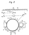
- an amorphous silicon type photoconductive layer 12 is formed on the surface of a metal drum 11 which is driven and rotated, and on the periphery of the drum 11, there are arranged, in the order recited, a corona charger 13 for main charging, an image light exposure mechanism comprising a lamp 14, an original-supporting transparent plate 15 and an optical system 16, a development mechanism 18 having a toner 17, a toner transfer corona charger 19, a paper-separating corona charger 20, a charge-removing lamp 21 and a cleaning mechanism 22.
- the photoconductive layer 12 is charged with a certain polarity by the corona charger 13. Then, an original 23 to be copied is irradiated by the lamp 14 through the contact glass 15, and the photoconductive layer 12 is exposed with the light image of the original through the optical system 16 to form an electrostatic latent image corresponding to the image of the original.
- This electrostatic latent image is developed with the toner 17 by the development mechanism 18.
- a transfer sheet 24 is supplied so that the sheet 24 is brought into contact with the drum surface at the position of the toner transfer charger 19, and corona charging is effected with the same polarity as that of the electrostatic latent image from the back of the transfer sheet 24 to transfer the toner image onto the transfer sheet 24.
- the transfer sheet 24 having the toner image transferred thereon is electrostatically peeled from the drum by the charge-removing action of the separating corona charger 20 and is then fed to a treating zone such as a fixing zone (not shown).
- the photoconductive layer 12 After transfer of the toner image, the photoconductive layer 12 is entirely exposed to light by the charge-removing lamp 21 to erase the residual charge, and the residual toner is removed by the cleaning mechanism 22.
- the amorphous silicon photosensitive layer 12 used in the present invention shows such a light fatigue as cannot be neglected, and the charge potential of the photosensitive layer after the light exposure is reduced by 20% at most based on the charge potential of the non-exposed portion of the photosensitive layer, and the image density of the print obtained at the second or subsequent operation is greatly different from the image density of the first formed-print.
- the present invention is based on the novel finding that the light fatigue of the amorphous silicon type photoconductive layer is greatly influenced by the wavelength of the light to which the photoconductive layer is exposed and by carrying out the light exposure in a spectral wavelength region having a wavelength shorter than 600 nm, the problem of the image memory owing to the light fatigue is obviated and images can be obtained at a certain high density.
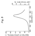
- Figure 3 is a graph showing the dependency of the light fatigue on the wavelength, and the wavelength at the light exposure of the photosensitive layer is plotted on the abscissa and the quantity or degree of reduction of the surface potential (light fatigue ratio, %) is plotted on the ordinate (the initial surface potential is 400 V). From Figure 3, it is seen that the light fatigue of amorphous silicon depends greatly on the wavelength of the light, and a maximum fatigue occurs at a wavelength of 725 nm and no substantial fatigue takes place to rays having a wavelength shorter than 600 nm.
- Figure 4 is a curve showing the spectral sensitivity of amorphous silicon, and it is seen that the sensitivity is drastically reduced at a wavelength larger than 850 nm.
- the present invention by using rays having a wavelength smaller than 600 nm for the light exposure, the light fatigue of an amorphous silicon type photoconductive layer is prevented and occurrence of the phenomenon of the image memory is effectively reduced.
- a laminate multilayer film 51 (see Figure 5) comprising two dielectric material layers differing in the refractive index is formed, instead of a silver or aluminum vacuum-deposited layer, as a reflecting mirror surface on at least one of mirrors 16A, 16B, 16C,... for the copying machine (see Figure 2), so that rays having a wavelength of at least 600 nm are allowed to pass through the reflecting mirror but rays having a wavelength shorter than 600 nm are reflected.
- the dielectric film formed on the mirror for the copying machine in order to allow transmission of rays having a wavelength of at least 600 nm, there is used a laminate of a film of ZnS, SiO or Ce0 2 and a film of MgF 2 , cryolite or Sn0 2 , and a combination of ZnS and MgF2 is especially preferred.
- These dielectric films are formed on the mirror by vacuum deposition.
- the thickness of the dielectric film layers are appropriately determined according to the kinds of dielectric materials so that rays having a wavelength of at least 600 nm are transmitted.
- the kind of the mirror for the copying machine, on which a dielectric film laminate as described above is formed, is not particularly critical, so far as the imagewise light exposure is effected with rays having a wavelength shorter than 600 nm, but it is especially preferred that the dielectric film laminate be formed on a mirror for the copying machine which is designed so that the incident angle of the rays is 45°.
- the multilayer film 51 of dielectric materials may be formed on at least one of lenses 16a, 16b, 16c,... for the copying machine. If this lens is used so that only rays having a wavelength shorter than 600 nm are passed through the lens, only rays having a wavelength shorter than 600 nm make contributions to the imagewise light exposure.
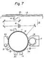
- an interference filter 61 is arranged in a light path in the optical system 16 to block up rays having a wavelength of at least 600 nm (see Figure 7).
- a laminate of a film of ZnS, SiO or Ce0 2 and a film of MgF 2 , cryolite or Sn0 2 is used as the interference filter, and a combination of ZnS and MgF 2 and especially preferred.
- These dielectric films are formed on a transparent glass or film by vacuum deposition.
- the thicknesses of the respective dielectric films are appropriately determined according to the kinds of the dielectric materials so that rays having a wavelength of at least 600 nm are blocked up.
- the imagewise light exposure is carried out by using a light source 14 having an emission spectrum of a wavelength shorter than 600 nm, whereby the light fatigue of the amorphous silicon type photoconductive layer is prevented and occurrence of the phenomenon of the image memory is effectively prevented.
- the light source 14 there can be mentioned, for example, a fluorescent lamp, a green fluorescent lamp, a blue fluorescent lamp, a green neon lamp and a green light-emitting diode. Since a halogen lamp customarily used as the light source for the copying machine includes rays having a longer wavelength, as pointed out hereinbefore, the light fatigue of the photoconductive layer 12 is violent.
- a color glass absorbing red rays and near infrared rays is used as the contact glass 15, and the light exposure is effected substantially by rays having a wavelength shorter than 600 nm.
- a blue glass can be used as the color glass, or such a color glass may be bonded to a transparent contact glass.
- amorphous silicon type photoconductive layers can be used in the present invention.
- amorphous silicon formed on a substrate by plasma decomposition of a silane glass may be used, and this silicon may be doped with hydrogen or halogen or doped with an element of the group III or V of the Periodic Table, such as boron or phosphorus.
- Physical values of a typical amorphous silicon photosensitive material are a dark conductivity of up to 10 -12 ⁇ -1 . cm- 1 , an activating energy smaller than 0.85 eV, a photoconductivity higher than 10 -7 ⁇ -1 . cm- 1 and an optical handicap of 1.7 to 1.9 eV, and the amount of combined hydrogen is 15 to 20 atomic % and the dielectric constant of a film of this photosensitive material is 11.5 to 12.5.
- an absorbing layer may be formed on the electroconductive substrate side to effectively retain the surface charge.
- the absorbing layer is doped with the same dopant as used for the photoconductive layer at a concentration much higher than in the photoconductive layer.
- a protecting layer of ⁇ -SiX C1-x, a-siN x or the like may be formed on the amorphous photoconductive layer 12.
- S600 represents the photosensitivity to a ray having a wavelength of 600 nm
- Smin represents a minimum photosensitivity to rays having a wavelength shorter than 500 nm (visible region).
- the above-mentioned effect may probably be due to the following mechanism.
- a carrier is produced in the vicinity of the surface of the amorphous silicon type photoconductive layer 12 or in the surface protecting layer by the short-wavelength component contained in the exposure light, and if the spectral sensitivity of the surface protecting layer is low, the carrier stays in this surface protecting layer.
- the absorption of rays having a short wavelength is increased with increase of the value x but the carrier range is narrowed, and hence, the photosensitivity to rays in the short wavelength region is ordinarily reduced as a whole.
- the thickness of the protecting layer for controlling this reduction is 1 pm, at most, and the reduction of the photosensitivity is controlled by doping with B or P. Consequently, in case of positive charging, the short wavelength sensitivity is determined by three factors, that is, the value x, the film thickness and the amount doped of the dopant B.
- the surface protecting layer satisfying the requirement of the above formula there can be mentioned, for example, a layer having a thickness of 0.1 um, which is composed of a-S o.6 Ni o.4 and is doped with 500 ppm of B.
- the value Smin/S600 is 0.91.
- the wavelength value Smin is hardly changed whether the alloying component is C, N or 0.
- reference numeral 71 represents an electroconductive substrate of Al
- reference numeral 72 represents a photosensitive layer of a-si:H
- reference numeral 73 represents a surface protecting layer composed of a-Si 1-x N x :B.
- a photosensitive material (a), (b) or (c) having this layer structure and a composition shown in Table 1 was attached to a commercially available electrostatic copying machine (Model DC-211 supplied by Mita Industrial Co.).
- a cold cathode discharge tube of a green color was used as the charge-removing light source, and as shown in Figure 5, ZnS and MgF 2 were alternately vacuum-deposited on a glass substrate 52 as a vacuum-deposited multilayer 51 on one surface of a copying mirror 16A for cutting rays having a wavelength of at least 600 nm, so that the incident angle of rays for the light exposure was 45°.
- the original used at the experiments had a size of A-3, and as shown in Figure 1-A, the original had a black solid letter part 3 having a reflection density of 1.5 in the former portion and an intermediate black solid part 2 having a reflection density of 0.8 in the latter portion.
- the value I in the original shown in Figure 1-A was adjusted to about 28 cm which was equal to the circumferential length of the drum having a diameter of 90 mm.
- a vacuum deposition multilayer 51' was formed on one surface of the copying lens 16a, instead of the copying mirror in Example 1, by alternately vacuum-depositing ZnS and MgF2, so that rays having a wavelength of at least 600 nm were cut.
- An a-Si:H layer (doped with 200 ppm of B) having a thickness of 0.1 pm was disposed as the blocking layer between the substrate 71 and the photoconductive layer 72 in the photosensitive drum (a), (b) or (c) used in Example 1.
- a green fluorescent lamp was disposed as the light source for the light exposure instead of provision of the dielectric layer on the mirror of the copying machine in Example 1.
- the relative emission spectrum of this green fluorescent lamp is shown in Figure 11.
- a bluish green color glass was used as the contact glass instead of provision of the dielectric layer on the mirror of the copying machine in Example 1.
- the spectral percent transmission of this color glass is shown in Figure 12.
Landscapes
- Physics & Mathematics (AREA)
- General Physics & Mathematics (AREA)
- Exposure Or Original Feeding In Electrophotography (AREA)
- Photoreceptors In Electrophotography (AREA)
Claims (7)
Applications Claiming Priority (10)
| Application Number | Priority Date | Filing Date | Title |
|---|---|---|---|
| JP43386/84U | 1984-03-28 | ||
| JP43382/84U | 1984-03-28 | ||
| JP4338584U JPS60156568U (ja) | 1984-03-28 | 1984-03-28 | 画像メモリ−の防止された複写機 |
| JP4338684U JPS60156569U (ja) | 1984-03-28 | 1984-03-28 | 画像メモリ−の防止された複写機 |
| JP43384/84U | 1984-03-28 | ||
| JP43385/84U | 1984-03-28 | ||
| JP4338284U JPS60156570U (ja) | 1984-03-28 | 1984-03-28 | 画像メモリ−の防止された複写機 |
| JP4338484U JPS60156567U (ja) | 1984-03-28 | 1984-03-28 | 画像メモリ−の防止された複写機 |
| JP43383/84U | 1984-03-28 | ||
| JP4338384U JPS60156566U (ja) | 1984-03-28 | 1984-03-28 | 画像メモリ−の防止された複写機 |
Publications (3)
| Publication Number | Publication Date |
|---|---|
| EP0157595A2 EP0157595A2 (fr) | 1985-10-09 |
| EP0157595A3 EP0157595A3 (en) | 1986-03-12 |
| EP0157595B1 true EP0157595B1 (fr) | 1990-01-03 |
Family
ID=27522312
Family Applications (1)
| Application Number | Title | Priority Date | Filing Date |
|---|---|---|---|
| EP85302149A Expired EP0157595B1 (fr) | 1984-03-28 | 1985-03-27 | Machine à copier avec une mémoire d'images réduite |
Country Status (3)
| Country | Link |
|---|---|
| US (1) | US4592643A (fr) |
| EP (1) | EP0157595B1 (fr) |
| DE (1) | DE3575211D1 (fr) |
Families Citing this family (3)
| Publication number | Priority date | Publication date | Assignee | Title |
|---|---|---|---|---|
| US4669855A (en) * | 1984-03-28 | 1987-06-02 | Konishiroku Photo Industry Co., Ltd. | Electrophotographic apparatus for obtaining visible images by irradiation of an amorphous silicon photosensitive member and method therefore |
| US5299632A (en) * | 1993-02-19 | 1994-04-05 | Lee Lien Jung | Fin device for an integrated circuit |
| JPH11305557A (ja) * | 1998-04-17 | 1999-11-05 | Fuji Xerox Co Ltd | 画像形成方法、画像形成装置および中間転写体 |
Family Cites Families (8)
| Publication number | Priority date | Publication date | Assignee | Title |
|---|---|---|---|---|
| US3511649A (en) * | 1966-05-02 | 1970-05-12 | Xerox Corp | Process of reducing fatigue in photoconductive glasses |
| US4132477A (en) * | 1975-12-27 | 1979-01-02 | Ricoh Company, Ltd. | Optical imaging system for electrophotography |
| DE2746967C2 (de) * | 1977-10-19 | 1981-09-24 | Siemens AG, 1000 Berlin und 8000 München | Elektrofotographische Aufzeichnungstrommel |
| JPS5480738A (en) * | 1977-12-09 | 1979-06-27 | Canon Inc | Optical system for copying apparatus |
| US4522485A (en) * | 1978-04-24 | 1985-06-11 | Canon Kabushiki Kaisha | Copying machine including a dielectric covered metal reflective device |
| JPS55137548A (en) * | 1979-04-13 | 1980-10-27 | Canon Inc | Method and apparatus for image formation |
| JPS56150752A (en) * | 1980-04-25 | 1981-11-21 | Hitachi Ltd | Electrophotographic sensitive film |
| JPS5918965A (ja) * | 1982-07-23 | 1984-01-31 | Fuji Xerox Co Ltd | 複写機の露光量検出装置 |
-
1985
- 1985-03-27 EP EP85302149A patent/EP0157595B1/fr not_active Expired
- 1985-03-27 DE DE8585302149T patent/DE3575211D1/de not_active Expired - Lifetime
- 1985-03-28 US US06/716,996 patent/US4592643A/en not_active Expired - Lifetime
Also Published As
| Publication number | Publication date |
|---|---|
| US4592643A (en) | 1986-06-03 |
| DE3575211D1 (de) | 1990-02-08 |
| EP0157595A2 (fr) | 1985-10-09 |
| EP0157595A3 (en) | 1986-03-12 |
Similar Documents
| Publication | Publication Date | Title |
|---|---|---|
| US3655377A (en) | Tri-layered selenium doped photoreceptor | |
| US4335194A (en) | Two color electrophotographic process and material | |
| JP2829629B2 (ja) | アモルファスシリコン系感光体を用いた電子写真法による画像形成方法及び電子写真装置 | |
| US4785324A (en) | Electrophotographic apparatus and method for preventing the lowering of a charging voltage at a photoreceptor | |
| EP0163415B1 (fr) | Substrat pour un élément photorécepteur et élément photorécepteur le contenant | |
| US5729800A (en) | Electrophotographic apparatus having an a-Si photosensitive drum assembled therein | |
| EP0157595B1 (fr) | Machine à copier avec une mémoire d'images réduite | |
| US4524117A (en) | Electrophotographic method for the formation of two-colored images | |
| US4433038A (en) | Electrophotographic copying process involving simultaneous charging and imaging | |
| US4420547A (en) | Photosensitive member for electrophotography having ultraviolet absorption layer | |
| JPH07120953A (ja) | 電子写真感光体およびそれを用いた画像形成方法 | |
| US5268247A (en) | Electrophotographic copying machine and electrophotographic member therefor and method of forming an electrophotographic member | |
| CA1142789A (fr) | Cliche electrophotographique, et methode de preparation connexe | |
| US4442191A (en) | Electrophotographic copying process for producing a plurality of copies | |
| US4440844A (en) | Electrophotographic copying process involving simultaneous charging and imaging | |
| GB1595463A (en) | Electrophotographic process | |
| JP3483375B2 (ja) | 光受容部材及びそれを用いた電子写真装置 | |
| US5087543A (en) | Electrophotographic printer | |
| US4440843A (en) | Electrophotographic copying process for forming positive or negative images | |
| EP0987576B1 (fr) | Appareil électrophotographique et méthode électrophotographique | |
| US4669855A (en) | Electrophotographic apparatus for obtaining visible images by irradiation of an amorphous silicon photosensitive member and method therefore | |
| US4717635A (en) | Electrophotographic recording material | |
| US4705735A (en) | Member having substrate with protruding surface portions and light receiving layer with amorphous silicon matrix | |
| JP2913066B2 (ja) | 電子写真感光体 | |
| JP3878752B2 (ja) | 画像形成装置 |
Legal Events
| Date | Code | Title | Description |
|---|---|---|---|
| PUAI | Public reference made under article 153(3) epc to a published international application that has entered the european phase |
Free format text: ORIGINAL CODE: 0009012 |
|
| AK | Designated contracting states |
Designated state(s): DE FR GB NL |
|
| PUAL | Search report despatched |
Free format text: ORIGINAL CODE: 0009013 |
|
| AK | Designated contracting states |
Kind code of ref document: A3 Designated state(s): DE FR GB NL |
|
| 17P | Request for examination filed |
Effective date: 19860430 |
|
| 17Q | First examination report despatched |
Effective date: 19871008 |
|
| GRAA | (expected) grant |
Free format text: ORIGINAL CODE: 0009210 |
|
| AK | Designated contracting states |
Kind code of ref document: B1 Designated state(s): DE FR GB NL |
|
| ET | Fr: translation filed | ||
| REF | Corresponds to: |
Ref document number: 3575211 Country of ref document: DE Date of ref document: 19900208 |
|
| PLBE | No opposition filed within time limit |
Free format text: ORIGINAL CODE: 0009261 |
|
| STAA | Information on the status of an ep patent application or granted ep patent |
Free format text: STATUS: NO OPPOSITION FILED WITHIN TIME LIMIT |
|
| 26N | No opposition filed | ||
| PGFP | Annual fee paid to national office [announced via postgrant information from national office to epo] |
Ref country code: NL Payment date: 19970327 Year of fee payment: 13 |
|
| PGFP | Annual fee paid to national office [announced via postgrant information from national office to epo] |
Ref country code: FR Payment date: 19980310 Year of fee payment: 14 |
|
| PGFP | Annual fee paid to national office [announced via postgrant information from national office to epo] |
Ref country code: GB Payment date: 19980318 Year of fee payment: 14 |
|
| PGFP | Annual fee paid to national office [announced via postgrant information from national office to epo] |
Ref country code: DE Payment date: 19980403 Year of fee payment: 14 |
|
| PG25 | Lapsed in a contracting state [announced via postgrant information from national office to epo] |
Ref country code: NL Free format text: LAPSE BECAUSE OF NON-PAYMENT OF DUE FEES Effective date: 19981001 |
|
| NLV4 | Nl: lapsed or anulled due to non-payment of the annual fee |
Effective date: 19981001 |
|
| PG25 | Lapsed in a contracting state [announced via postgrant information from national office to epo] |
Ref country code: GB Free format text: LAPSE BECAUSE OF NON-PAYMENT OF DUE FEES Effective date: 19990327 |
|
| GBPC | Gb: european patent ceased through non-payment of renewal fee |
Effective date: 19990327 |
|
| PG25 | Lapsed in a contracting state [announced via postgrant information from national office to epo] |
Ref country code: FR Free format text: LAPSE BECAUSE OF NON-PAYMENT OF DUE FEES Effective date: 19991130 |
|
| REG | Reference to a national code |
Ref country code: FR Ref legal event code: ST |
|
| PG25 | Lapsed in a contracting state [announced via postgrant information from national office to epo] |
Ref country code: DE Free format text: LAPSE BECAUSE OF NON-PAYMENT OF DUE FEES Effective date: 20000101 |