EP0158357A2 - Procédé pour réaliser des structures microréserve - Google Patents
Procédé pour réaliser des structures microréserve Download PDFInfo
- Publication number
- EP0158357A2 EP0158357A2 EP85104417A EP85104417A EP0158357A2 EP 0158357 A2 EP0158357 A2 EP 0158357A2 EP 85104417 A EP85104417 A EP 85104417A EP 85104417 A EP85104417 A EP 85104417A EP 0158357 A2 EP0158357 A2 EP 0158357A2
- Authority
- EP
- European Patent Office
- Prior art keywords
- resist
- pattern
- layer
- mask
- etching
- Prior art date
- Legal status (The legal status is an assumption and is not a legal conclusion. Google has not performed a legal analysis and makes no representation as to the accuracy of the status listed.)
- Granted
Links
Images



Classifications
-
- G—PHYSICS
- G03—PHOTOGRAPHY; CINEMATOGRAPHY; ANALOGOUS TECHNIQUES USING WAVES OTHER THAN OPTICAL WAVES; ELECTROGRAPHY; HOLOGRAPHY
- G03F—PHOTOMECHANICAL PRODUCTION OF TEXTURED OR PATTERNED SURFACES, e.g. FOR PRINTING, FOR PROCESSING OF SEMICONDUCTOR DEVICES; MATERIALS THEREFOR; ORIGINALS THEREFOR; APPARATUS SPECIALLY ADAPTED THEREFOR
- G03F7/00—Photomechanical, e.g. photolithographic, production of textured or patterned surfaces, e.g. printing surfaces; Materials therefor, e.g. comprising photoresists; Apparatus specially adapted therefor
- G03F7/26—Processing photosensitive materials; Apparatus therefor
- G03F7/40—Treatment after imagewise removal, e.g. baking
-
- G—PHYSICS
- G03—PHOTOGRAPHY; CINEMATOGRAPHY; ANALOGOUS TECHNIQUES USING WAVES OTHER THAN OPTICAL WAVES; ELECTROGRAPHY; HOLOGRAPHY
- G03F—PHOTOMECHANICAL PRODUCTION OF TEXTURED OR PATTERNED SURFACES, e.g. FOR PRINTING, FOR PROCESSING OF SEMICONDUCTOR DEVICES; MATERIALS THEREFOR; ORIGINALS THEREFOR; APPARATUS SPECIALLY ADAPTED THEREFOR
- G03F7/00—Photomechanical, e.g. photolithographic, production of textured or patterned surfaces, e.g. printing surfaces; Materials therefor, e.g. comprising photoresists; Apparatus specially adapted therefor
- G03F7/0035—Multiple processes, e.g. applying a further resist layer on an already in a previously step, processed pattern or textured surface
-
- Y—GENERAL TAGGING OF NEW TECHNOLOGICAL DEVELOPMENTS; GENERAL TAGGING OF CROSS-SECTIONAL TECHNOLOGIES SPANNING OVER SEVERAL SECTIONS OF THE IPC; TECHNICAL SUBJECTS COVERED BY FORMER USPC CROSS-REFERENCE ART COLLECTIONS [XRACs] AND DIGESTS
- Y10—TECHNICAL SUBJECTS COVERED BY FORMER USPC
- Y10S—TECHNICAL SUBJECTS COVERED BY FORMER USPC CROSS-REFERENCE ART COLLECTIONS [XRACs] AND DIGESTS
- Y10S430/00—Radiation imagery chemistry: process, composition, or product thereof
- Y10S430/143—Electron beam
-
- Y—GENERAL TAGGING OF NEW TECHNOLOGICAL DEVELOPMENTS; GENERAL TAGGING OF CROSS-SECTIONAL TECHNOLOGIES SPANNING OVER SEVERAL SECTIONS OF THE IPC; TECHNICAL SUBJECTS COVERED BY FORMER USPC CROSS-REFERENCE ART COLLECTIONS [XRACs] AND DIGESTS
- Y10—TECHNICAL SUBJECTS COVERED BY FORMER USPC
- Y10S—TECHNICAL SUBJECTS COVERED BY FORMER USPC CROSS-REFERENCE ART COLLECTIONS [XRACs] AND DIGESTS
- Y10S430/00—Radiation imagery chemistry: process, composition, or product thereof
- Y10S430/167—X-ray
- Y10S430/168—X-ray exposure process
Definitions
- the present invention relates to a method of forming a resist pattern and, more particularly, to a method of forming a resist micropattern on a substrate with high precision in a relatively short period of time.
- a conventional simultaneous pattern transfer technique has been used as a means for forming a pattern of semiconductor ICs or the like on a substrate by using a mask.
- a film of a resin material, i.e., a resist sensitive (crosslinked or decomposed) to an energy beam is formed, and an energy beam carrying pattern information, such as light, irradiates (i.e., exposes) the resist film which is then developed to obtain a resist pattern.
- the semiconductor substrate is processed using the resultant resist pattern.
- the resolution of the pattern to be formed is degraded due to the diffraction phenomenon. For this reason, high energy beams such as electron beams or X-rays are effectively used for fine lithography. However, even if such a high energy beam is used, the resolution of the resultant pattern is still low.
- an electron beam is used as an energy beam and a positive electron beam resist material is used as a resist material to form a resist pattern.
- the electron beam irradiates a positive electron beam resist film on a semiconductor substrate in an amount such that the resist film can respond to the beam, i.e., decomposed, along the direction of the entire thickness thereof.
- the electrons which enter into the resist film and the substrate collide with molecules and atoms thereof and are scattered back out of the substrate.
- a scattering distance of these electrons generally falls within the range of several microns to several tens of microns although the distance varies depending on an energy level of the irradiated electron beam and a density of the substrate.
- the positive resist material responds to the beam again.
- an area of the positive resist film decomposed by the beam is larger than an incident beam size (i.e., a beam profile) of the electron beam.
- a resist pattern When the exposed resist film is developed under the above condition, a resist pattern has a size larger than that of the electron beam.
- the pattern density is high, its resolution is greatly degraded by the back-scattered electrons generated when an adjacent pattern is irradiated with the electron beam.
- the above situation also applies to the degradation of resolution due to the presence of the substrate such as the generation of secondary electrons in X-ray lithography leading to the degradation of resolution, or the generation of a standing wave in photolithography leading to pattern edge nonuniformity.
- an object of the present invention to provide a method of forming a resist pattern on the basis of energy beam exposure, wherein a desired resist micropattern can be formed with high precision in a relatively short period of time.
- a method of forming a resist pattern on a substrate comprising the steps of:
- the first appearing interface between the mask layer and the resist is detected by using a label material.
- the energy beams include light, electron beams, X-rays and ion beams.
- the present inventors have paid attention to the fact that the degradation of the pattern in energy beam exposure resulted from the following:
- Figs. lA to lE show a first embodiment of the present invention, wherein electron beams are used as energy beams and an electron beam resist material is used as a resist material.
- a layer 12 of an electron beam resist material is formed on a semiconductor wafer such as a silicon wafer 11 to a thickness of, for example, about I ⁇ m to 2 pm.
- a positive or negative electron beam resist material can be used. However, a positive resist material is preferable since it has higher resolution than a negative resist material.
- the positive electron beam resist material includes those which are irradiated by the energy beam, and are then developed by developer, such as polymethylmethacrylate (PMMA), polyhexafluoro- butylmethacrylate CFBM-G), and a phenylmethacrylate-methacrylic acid copolymer ( ⁇ -MAC) and those in which the electron beam serves as exposure and development, i.e., the resist material is completely decomposed and volatilizes by radiation of the electron beams alone, and the recessed pattern can be formed without using the developer.
- PMMA polymethylmethacrylate
- CFBM-G polyhexafluoro- butylmethacrylate
- ⁇ -MAC phenylmethacrylate-methacrylic acid copolymer
- arylmethacrylate e.g., a,a-dimethylbenzyl methacrylate, a-methylbenzyl methacrylate, diphenyl methacrylate, triphenyl methacrylate, and phenyl me
- Electron beams EB carrying predetermined pattern information irradiate the layer 12.
- the dose is sufficiently smaller than that required for exposing the layer 12 throughout its entire thickness. More particularly, the dose is determined such that the bottom of the recessed pattern formed in the layer 12 after its development does not reach the surface of the substrate 11.
- the dose varies in accordance with the type of the resist material, but is generally about 1/5 to 1/10 of the dose required for forming the recessed pattern throughout the layer 12.
- a recessed pattern 13 in the upper layer portion of the layer 12, as shown in Fig. 1B.
- the pattern 13 properly reflects the beam profile of the beams EB.
- Depths of concaves of the pattern 13 are preferably 0.4 ⁇ m or less, and more preferably 0.15 to 0.4 ⁇ m.
- dose of electron beams required to form a recessed pattern having a concave depth of 0.2 ⁇ m in a resist material layer having a thickness of 1 ⁇ m at an acceleration voltage of 30 KeV are summarized in Table 1.
- a layer 14 of a mask material which has high resistance to the etchant of the material of the layer 12 is formed to cover the entire surface including the pattern 13 so as to provide a flat surface 15, as shown in Fig. 1C.
- the mask material used has an etching rate lower than that of the resist material used (generally, 1/10 or less).
- the mask material includes a material such as silicone resin or spin-on glass which is coated with a spin coater or a material such as amorphous silicon, polyimide resin or carbon which is deposited by reduced pressure deposition.
- a preferable mask material is silicone resin.
- silicone resin as a mask material is applied to the layer 12 having the recessed pattern with a concave depth of 0.4 ⁇ m and a width W.
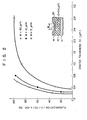
- smoothness as a percentage of a ratio (t 1 /t 0 ) of a silicon resin thickness t 1 at concave of the layer 12 to a silicone resin thickness to at the flat surface of the resist layer 12 is plotted as a function of the silicone resin thickness t 0 by using the recessed pattern width W as a parameter, as shown in Fig. 2.
- planarization (t 1 /t 0 ) is 100%, the silicone resin has a flat top surface.
- Fig. 2 shows that when silicone resin is applied to a thickness of 2.0 um or more, the surface of the silicon resin can be planarized even over a wide recess.
- the layer 14 is uniformly etched along the direction of its thickness. This etching can be performed by reactive ion etching. The etching of the layer 14 is performed until at least the top surface of the layer 12 is exposed. Preferably, as shown in Fig. lD, the mask is etched back by a depth corresponding to half of the entire depth of each recess (concave). When the layer 12 is etched using a residual mask pattern 16, the resist pattern width more properly reflects the electron beam size.
- the layer 12 is etched by anisotropic etching such as reactive ion etching using the pattern 16 as a mask until the surface of the substrate 11 is exposed.
- anisotropic etching such as reactive ion etching
- the substrate 11 is processed using the pattern 17 as a mask.
- the above method is exemplified wherein the electron beam is used as a pattern information carrier and a predetermined resist pattern is formed in the electron beam resist material.
- a photoresist material e.g., AZ 1350J
- an X-ray resist material e.g., FBM-G
- an ion beam resist material e.g., PMMA
- the dose of the energy beam irradiating the layer 12 so as to form the pattern 13 is sufficiently smaller (about 1/5 to 1/10) than the conventional dose. Therefore, the influences of a substrate, such as generation of back-scattered electrons, secondary electrons and the standing wave, can be eliminated and a resist micropattern can be formed with high precision. In addition, the dose of the energy beam is small, and thus the radiation time can be shortened. When electron beams are used, a resist layer can be irradiated with beams of the same size as the predetermined pattern, thereby improving the throughput.
- the influences of a substrate can be eliminated as described above upon radiation of the energy beams, so that an isolated independent recessed pattern (i.e., a single line pattern) and a dense recessed pattern (i.e., a line and space pattern) can be formed with the same high precision.
- the energy beam doses required to form the single line pattern and the line and space pattern with the same concave depth slightly differ from each other.
- the depth of the recess (concave) is 0.4 ⁇ m or less, a recessed pattern wherein the single line pattern and the line and space pattern are co-present can be formed with the same given energy beam dose, resulting in convenience.
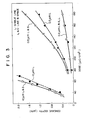
- the relationship between the electron beam dose and the depth of the recess is shown when the single line patterns and the line and space patterns having line widths of 10 um, 0.5 um and 0.2 ⁇ m are formed in a PMMA resist layer on a silicon substrate.
- the single line recessed pattern and the line and space recessed pattern can be formed by irradiation of electron beams in substantially the same dose.
- ⁇ -MAC phenylmethacrylate-methacrylic acid copolymer
- a recessed pattern having a depth of 0.15 ⁇ m to 0.2 ⁇ m and properly reflecting the beam size was formed in the surface portion of the resist film.
- silicone resin was applied by a spin coater to the entire surface of the resist film to a thickness of 0.6 pm.
- the surface of the sample became flat.
- the resultant sample was etched in a reactive ion etching apparatus at a power density of 0.3 W/cm 2 for 12 minutes while CF 4 gas flowed at a rate of 50 sccm.
- silicone resin was etched uniformly from the surface of the resin along the direction of its thickness to a depth corresponding to half of the depth of the recess of the recessed pattern.
- the sample was etched in the reactive ion etching apparatus again at a power density of 0.3 W/cm 2 for 10 minutes while 0 2 gas flowed at a rate of 50 sccm.
- a resist pattern having a high aspect ratio was formed under the silicone resin pattern.
- the silicone resin pattern was not substantially etched, and only ⁇ -MAC was etched.
- the resultant pattern size properly reflected the beam size and the size precision was 0.05 ⁇ m or less.
- the resist pattern with high precision was obtained according to Example 1.
- This example shows a case wherein exposure with light is used.
- a recessed pattern was transferred to a positive resist AZ 1350J through a photomask having a pattern with a width of 1 pm.
- the dose was 6 mJ/cm 2 which was about 1/10 of the conventional dose.
- the g line (0.436 ⁇ m) was used as the wavelength of light for radiation.
- Silicone resin was then applied to the sample and etched in the reactive ion etching apparatus in the same manner as in Example 1.
- the silicone resin layer was lightly over-etched to an about 50 nm above the bottom of the recess.
- the resist material on the sample was etched in the same manner as in Example 1.
- the resultant resist pattern had a width of 0.8 pm which was smaller than the photomask width.
- the resist pattern having a smaller size than that of the designed. pattern could be obtained.
- the recessed pattern was formed with a dose which was about 1/10 of the conventional dose, thereby greatly shortening the processing time.
- Example 3 a polymer film of poly a,a-dimethylbenzylmethacrylate was applied to a silicon wafer to a thickness of 1 ⁇ m. Electron beams were irradiated on the sample at a dose of 20 ⁇ C/cm 2 to form a recessed pattern having a depth of 0.2 um. Silicone resin was applied to the entire surface of the sample to provide a flat surface, and the silicone resin film and the polymer film were etched in the same manner as in Example 1, thereby obtaining a resist pattern having a width of 1 um which was the same as the beam size. In the above resist material, main and side chains of the copolymer were dissociated and the molecules were evaporated upon radiation of the electron beams in a known manner. Therefore, the development process can be omitted to simplify the pattern formation process.
- Example 4 An amorphous silicon film was used in Example 4.
- the above-mentioned ⁇ -MAC was applied to a silicon wafer to a thickness of 1 pm, and a recessed pattern was formed with electron beams under the same exposure and development conditions.
- the amorphous silicon film was sputtered on the sample in a sputtering apparatus.
- the amorphous silicon film can be formed by a known RF sputtering technique at a rate of 0.1 um/10 minutes.
- the amorphous silicon film had a thickness of 0.6 ⁇ m.
- the surface of the amorphous silicon film was flat.
- the amorphous silicon film was etched in a parallel flat plate dry etching apparatus at a power density of 0.38 W/cm 2 for about 20 minutes while CCl 2 F 2 gas was flowed in at a rate of 20 sccm.
- the amorphous silicon film was uniformly etched to a depth corresponding to half of the depth of the recessed pattern.
- the ⁇ -MAC was etched in the 0 2 atmosphere by using the residual amorphous silicon pattern as a mask, thereby forming a resist pattern under the amorphous silicon pattern.
- a detecting means e.g., a'mass or emission spectroscope
- a label material are provided for detecting an interface between the top portion of the layer 12 which is exposed first and the layer 14 when the layer 14 is etched.
- the surface of the residual mask layer 14 has the same level as that of the resist layer 12.
- the etching depth is controlled by an etching time calculated in accordance with the etching rate of the mask material and the thickness of the residual mask material.
- the mask material layer left in the recessed pattern formed in the layer 12 has a very small thickness (e.g., 0.4 ⁇ m or less) corresponding to the depth of each recess. Therefore, the pattern 16 can be obtained with very high precision even when the etching is controlled by the calculated etching time.
- the same techniques as in the first embodiment can be used except for the interface detection. Therefore, the preferred techniques in the first embodiment can also be applied to the second embodiment.
- Figs. 4A to 4C collectively show a first sub-embodiment of the second embodiment.
- a label material is mixed beforehand in a resist material when a resist material layer 12 is formed on a substrate 11.
- the label material is defined as a material having an element different from those constituting the resist and mask materials.
- the interface is detected by detecting changes in a mass or emission spectrum of the element of the label material.
- the label material is preferably a metal compound compatible with the resist material.
- the metal compound includes an inorganic metal compound such as zinc halide (e.g., zinc bromide) and an organic metal compound such as an organic aluminum compound (e.g., aluminum tert-butylate, aluminum acetylacetonate, or polymethylaluminoxane).
- an inorganic metal compound such as zinc halide (e.g., zinc bromide)
- an organic metal compound such as an organic aluminum compound (e.g., aluminum tert-butylate, aluminum acetylacetonate, or polymethylaluminoxane).
- concentration of such a label material is 1 to 10% by weight.
- a resist material containing the label material is applied to the substrate 11, in the same manner as described with reference to Fig. lA, to form a resist layer 12'.
- energy beams such as electron beams are irradiated on the resultant structure to form a recessed pattern 13.
- a mask layer 14 is formed on the layer 12' (Fig. 4A).
- the layer 14 is etched by reactive ion etching. During etching, the mass or emission spectrum of the metal element contained in the layer 12' is detected or monitored.
- the reactive ion etching apparatus used in the second embodiment is provided with a mass or emission spectroscope.
- a typical example is illustrated in Fig. 5.
- This apparatus 20 includes a vacuum chamber 21.
- Flat electrodes 22 and 23 are arranged in the chamber 21 to oppose each other and to be parallel to each other.
- An RF power source 24 is connected to the electrodes 22 and 23.
- the electrode 22 is grounded, and a structure S of Fig. 4A is placed on the electrode 23 such that the layer 14 is directed toward the electrode 22.
- a vacuum pump unit 25 and an etching gas supply source 26 are connected to the chamber 21.
- the apparatus 20 has the same construction as that of the conventional reactive ion etching apparatus, except that a mass or emission spectroscope 27 is arranged in the chamber 21.
- the spectroscope 27 is connected to a spectrum detector 28 outside the chamber 21.
- the detector 28 is connected to a recorder 29. Further, the detector 28 may have a construction which provides signals to controll the gass source 26 (or the valve V) and the RF power source 24, as indicated by broken line in Fig. 5.
- the layer z l4 is etched by the apparatus 20.
- the same etching technique as in the first embodiment is used, except that the metal element contained in the label material of the layer 12' is monitored by the spectroscope 27.
- the spectrum of the metal element of the label material contained in the layer 12' is abruptly increased, thereby indicating the interface.
- the surface of the layer 12' has the same level as that of the layer 14, as shown in Fig. 4B.
- the change in spectrum of the metal element is sharp, thereby allowing the interface to be detected with high precision.
- the pattern 16' is formed.
- etching is continued in accordance with the etching time calculated from the etching rate of the mask material and the thickness of the residual mask material. For example, when etching is performed for a time calculated in accordance with the etching rate of the mask material and 1/2 of the thickness of the residual mask film, the etching depth of the residual mask film is half that of the recess of the recessed pattern, as shown in Fig. 4C. Therefore, a mask pattern 16' with higher precision can be obtained in the same manner as in the mask pattern 16.
- the layer 12' is etched using the pattern 16' as an etching mask to obtain a resist pattern similar to the resist pattern 17 shown in Fig. lE, but with higher precision.
- the presence of the label material does not present any problem when the layer 12' is anisotropically etched.
- the label material is mixed in the resist layer.
- the label material may be mixed in the mask layer. In this case, the level of the spectrum of the metal element is abruptly decreased when the interface appears.
- Fig. 6 shows a second sub-embodiment of the second embodiment of the present invention.
- the second sub-embodiment differs from the first sub-embodiment in that the second sub-embodiment includes a step of coating a mixture of the resist or mask material and the label material on the resist layer to form a label layer 31, between the steps of forming the recessed pattern 13 in the resist layer and of forming the mask layer 14.
- the layer 12 is being etched, an interface between the layers 31 and 12 is exposed. In this state, the spectrum level based on the metal element contained in the label layer 31 can be detected.
- a thickness of the layer 31 is 0.1 to 0.2 um, and a concentration of the label material contained therein is I to 10% by weight.
- Figs. 7A to 7D collectively show a third sub-embodiment of the second embodiment.
- a first resist layer 12 is formed on a substrate 11, and a label layer 31' of a resist material mixed with the label material is formed to a thickness of, usually 0.05 to 0.15 pm.
- a second resist layer 12" is formed on the label layer 31' to a thickness of, usually, 0.1 to 0.2 ⁇ m (Fig. 7A).
- a total thickness of the layers 31' and 12" is less than 0.4 pm. The total thickness preferably falls within the range between 0.15 and 0.2 pm.
- a recessed pattern 13 is formed in the same manner as described with reference to Figs. 1A and 1B.
- the recessed pattern extends through the layer 31', as shown in Fig. 7B.
- a mask material layer 14 is formed on the surface of the structure of Fig. 7B and etched while the spectrum of the metal element of the label material is detected in the same manner as described wit> reference to Fig. 4A.
- the surface level of the residual material 16 is the same as that of the layer 31', as shown in Fig. 7D.
- the residual label layer and the resist material layer 12 are etched using a mask pattern 16 constituted by the residual mask material as an etching mask in the same manner as in the first embodiment wherein the layer 12 is etched, thereby obtaining a desired resist pattern.
- the label material is intentionally used.
- the interface detecting means is not limited to the technique using a label material.
- the element can be detected in the same manner as the label material to obtain the effect of the second embodiment.
- the surface of the resist material layer can be accurately detected, and a desired resist pattern can be formed with higher precision.
- a resist of phenylmethacrylate-methacrylic acid copolymer (#-MAC) containing 5% of ZnBr as a label material was coated on a silicon substrate to a thickness of 1.5 ⁇ m. The sample was then prebaked at a temperature of 200°C for an hour. Electron beams were irradiated on the sample which was then developed by a mixture of 25% of 1,4-dioxane and 75% of diisobutyl ketone to form a recessed pattern having a concave depth of 0.2 to 0.3 pm in the surface portion of the resist layer. As shown in Fig. 4A, silicone resin was spin-coated to cover the entire surface so as to obtain a flat surface.
- the entire surface of the substrate could be flattened.
- silicone resin was continuously etched for an etching time calculated from the etching rate of silicone resin and 1/2 of the thickness of the residual mask film. As shown in Fig. 4C, silicone resin was etched to a depth corresponding to 1/2 of the depth of each recess. In this case, the etching precision of silicone resin was 20 to 30 nm.
- the resist material on the sample was etched as in the same manner as in Example 1. As a result, the patterns were obtained with a precision of about 15 to 20 nm, thus providing size control with high precision.
- a polymethylmethacrylate (PMMA) resist was coated on a substrate to a thickness of 1.5 um and prebaked. Electron beams were irradiated on.the sample which was then developed by a mixture of methylisobutyl ketone and isopropanol to obtain a recessed pattern. The sample was then post-baked, and the resist ⁇ -MAC containing 5% of ZnBr as a label material was applied to the sample to a thickness of about 0.1 ⁇ m. After prebaking, the recessed pattern was flattened by coating it with a silicone resin.
- PMMA polymethylmethacrylate
- the silicone resin film was etched by reactive ion etching using CF 4 gas.
- the etching time was calculated from the etching rate of silicone resin and the thickness of the residual portion.
- size precision could be 0.05 um or less.
- the PMMA layer was etched using the residual mask material as an etching mask to obtain a resist pattern.
- the ZnBr-contained ⁇ -MAC was used as the label material in Example 6. However, this material may be used as the resist in place of PMMA.
- a PMMA resist was coated on a substrate 11 to a thickness of 1.5 um and prebaked.
- a dilute PMMA material obtained by dissolving an organic metal such as aluminum tert-butylate (Al(OC 4 H 9 ) 3 ) as a label material was applied to the sample to a thickness of 50 nm. PMMA was further coated on the sample to a thickness of 0.1 um and prebaked.
- the label material layer was sandwiched between the PMMA layers.
- the sample was irradiated with electron beams and then developed to obtain a recessed pattern 13 having a depth of 0.3 pm in the surface layer of the resist film, as shown in Fig. 7B.
- the width of the recessed pattern 13 properly reflected the beam profile.
- the label material layer located substantially at the center along the direction of thickness of the recessed pattern was very. thin and dissolved upon development of the PMMA layer.
- Silicone resin was then coated on the sample to flatten the surface. The silicone resin layer was etched by reactive ion etching using CF 4 and O 2 gases.
- etching conditions e.g., a CF 4 flow rate of 50 sccm, O 2 flow rate of 10 sccm, a pressure of 10 mTorr, and an RF power of 0.3 W/cm 2
- the etching state was monitored by the emission spectroscope 27 (Fig. 5).
- peaks having emission intensities which were five times that obtained by etching of silicone resin were obtained from aluminum at wavelengths of 3,082 A, 3,093 A, 3,944 A and 3,962 A, respectively.
- An organic metal such as aluminum acetylacetonate, Al(CH 2 COCH 2 -COCH 3 ) 3 or polymethylaluminoxane ( ⁇ CH 3 AlO) ⁇ n could be used as a label material to obtain the same effect as in Example 7.
- the label material was mixed in the resist material layer.
- a label material can be mixed in a mask material. Silicone resin and polyaminoxane were dissolved in ligroin in a ratio of 10:1, and the resultant mixture was used as a mask material.
- the recessed pattern formed in the surface portion of the PMMA layer was flattened by coating the mask material.
- the mask material was etched in the reactive ion etching using CF 4 gas, a strong emission spectrum at 3,082 'to 3,962 A was produced from the Al atoms contained in polyaluminoxane.
- the strength of emission from the mask material was decreased to 1/3 the initial strength, thereby indicating that none of the mask material remained on the flat portion of the PMMA layer.
- the mask material was etched to a depth corresponding to about 1/2 of the depth of the recessed pattern, thus providing pattern control with;high precision. Thereafter, the resist layer was etched using the residual mask material as an etching mask to form a resist pattern.
- a label material was not used in Example 9.
- a recessed pattern was formed with electron beams in the surface portion of the ⁇ -MAC resist film.
- Silicone resin was coated on the sample to flatten the surface thereof.
- the silicone resin layer was etched in the reactive ion etching apparatus using CF 4 and 0 2 (20%) gases.
- a mass spectrum was monitored by the spectroscope.
- the sample was further etched for 5 minutes to obtain a mask pattern with high precision.
- the present invention has been exemplified by a single layer resist.
- the resist is not limited thereto.
- the present invention can also be applied to a multi-layer resist.
- the steps as have been described above are applied to the uppermost resist layer.
- the present invention can also be applied to a two-layer resist comprising an uppermost layer of a positive resist material and underlying layer of a negative resist material.
- a predetermined recessed pattern is formed in the uppermost layer, and a mask material layer is formed thereon. Thereafter, the mask material is etched to form a mask pattern.
- the uppermost layer and the underlying layer are etched using the mask pattern (residual mask material layer) as a mask.
- the substrate can be processed with high precision.
Landscapes
- Physics & Mathematics (AREA)
- General Physics & Mathematics (AREA)
- Photosensitive Polymer And Photoresist Processing (AREA)
- Exposure And Positioning Against Photoresist Photosensitive Materials (AREA)
Applications Claiming Priority (4)
| Application Number | Priority Date | Filing Date | Title |
|---|---|---|---|
| JP59074690A JPS60218843A (ja) | 1984-04-13 | 1984-04-13 | パタン形成方法 |
| JP74690/84 | 1984-04-13 | ||
| JP60035692A JPS61194831A (ja) | 1985-02-25 | 1985-02-25 | パタン形成方法 |
| JP35692/85 | 1985-02-25 |
Publications (3)
| Publication Number | Publication Date |
|---|---|
| EP0158357A2 true EP0158357A2 (fr) | 1985-10-16 |
| EP0158357A3 EP0158357A3 (en) | 1987-10-28 |
| EP0158357B1 EP0158357B1 (fr) | 1991-02-27 |
Family
ID=26374686
Family Applications (1)
| Application Number | Title | Priority Date | Filing Date |
|---|---|---|---|
| EP85104417A Expired EP0158357B1 (fr) | 1984-04-13 | 1985-04-11 | Procédé pour réaliser des structures microréserve |
Country Status (4)
| Country | Link |
|---|---|
| US (1) | US4634645A (fr) |
| EP (1) | EP0158357B1 (fr) |
| CA (1) | CA1264596A (fr) |
| DE (1) | DE3581822D1 (fr) |
Cited By (3)
| Publication number | Priority date | Publication date | Assignee | Title |
|---|---|---|---|---|
| FR2672138A1 (fr) * | 1991-01-30 | 1992-07-31 | Samsung Electronics Co Ltd | Procede de formation d'un micromotif au-dessous de la limite de resolution d'un processus photolithographique. |
| EP0607680A3 (fr) * | 1992-12-22 | 1994-12-21 | Wisconsin Alumni Res Found | Fabrication de microstructures utilisant une couche formant photoréserve préformée. |
| WO1998020517A1 (fr) * | 1996-11-07 | 1998-05-14 | National University Of Singapore | Micro-usinage au moyen d'ions legers tres energetiques |
Families Citing this family (13)
| Publication number | Priority date | Publication date | Assignee | Title |
|---|---|---|---|---|
| JPS62140485A (ja) * | 1985-12-16 | 1987-06-24 | Hitachi Ltd | 半導体構造体およびその製造方法 |
| US4774164A (en) * | 1987-04-06 | 1988-09-27 | Tegal Corporation | Chrome mask etch |
| JPS6450425A (en) * | 1987-08-20 | 1989-02-27 | Toshiba Corp | Formation of fine pattern |
| US4769257A (en) * | 1987-10-09 | 1988-09-06 | Duley Walter W | Laser etching of foam substrate |
| US4933205A (en) * | 1987-10-09 | 1990-06-12 | Duley Walter W | Laser etching of foam substrate |
| US4972061A (en) * | 1987-12-17 | 1990-11-20 | Duley Walter W | Laser surface treatment |
| US5330879A (en) * | 1992-07-16 | 1994-07-19 | Micron Technology, Inc. | Method for fabrication of close-tolerance lines and sharp emission tips on a semiconductor wafer |
| KR0141941B1 (ko) * | 1994-11-11 | 1998-07-15 | 문정환 | 감광막의 패터닝방법 |
| JP2001125268A (ja) * | 1999-10-28 | 2001-05-11 | Sony Corp | 露光方法 |
| JP3415602B2 (ja) * | 2000-06-26 | 2003-06-09 | 鹿児島日本電気株式会社 | パターン形成方法 |
| KR100640640B1 (ko) | 2005-04-19 | 2006-10-31 | 삼성전자주식회사 | 미세 피치의 하드마스크를 이용한 반도체 소자의 미세 패턴형성 방법 |
| KR100740612B1 (ko) * | 2006-02-15 | 2007-07-18 | 삼성전자주식회사 | 반도체 장치 및 그 형성 방법 |
| KR100809597B1 (ko) * | 2006-04-06 | 2008-03-04 | 삼성전자주식회사 | 미세 패턴 형성 방법 및 이를 이용한 반도체 메모리 장치의형성 방법 |
Family Cites Families (8)
| Publication number | Priority date | Publication date | Assignee | Title |
|---|---|---|---|---|
| JPS4972A (fr) * | 1972-04-13 | 1974-01-05 | ||
| US4528438A (en) * | 1976-09-16 | 1985-07-09 | Northern Telecom Limited | End point control in plasma etching |
| US4275286A (en) * | 1978-12-04 | 1981-06-23 | Hughes Aircraft Company | Process and mask for ion beam etching of fine patterns |
| US4215935A (en) * | 1979-05-24 | 1980-08-05 | Loebach Ernst W | Method and device for the projection printing of a mask onto a semiconductor substrate |
| US4457820A (en) * | 1981-12-24 | 1984-07-03 | International Business Machines Corporation | Two step plasma etching |
| JPS5916978A (ja) * | 1982-07-20 | 1984-01-28 | Tokyo Denshi Kagaku Kabushiki | 金属被膜の選択的エツチング方法 |
| JPS59147433A (ja) * | 1983-02-14 | 1984-08-23 | Hitachi Ltd | エツチング装置 |
| US4546066A (en) * | 1983-09-27 | 1985-10-08 | International Business Machines Corporation | Method for forming narrow images on semiconductor substrates |
-
1985
- 1985-04-09 US US06/721,306 patent/US4634645A/en not_active Expired - Lifetime
- 1985-04-10 CA CA000478690A patent/CA1264596A/fr not_active Expired
- 1985-04-11 DE DE8585104417T patent/DE3581822D1/de not_active Expired - Lifetime
- 1985-04-11 EP EP85104417A patent/EP0158357B1/fr not_active Expired
Cited By (6)
| Publication number | Priority date | Publication date | Assignee | Title |
|---|---|---|---|---|
| FR2672138A1 (fr) * | 1991-01-30 | 1992-07-31 | Samsung Electronics Co Ltd | Procede de formation d'un micromotif au-dessous de la limite de resolution d'un processus photolithographique. |
| EP0607680A3 (fr) * | 1992-12-22 | 1994-12-21 | Wisconsin Alumni Res Found | Fabrication de microstructures utilisant une couche formant photoréserve préformée. |
| US5496668A (en) * | 1992-12-22 | 1996-03-05 | Wisconsin Alumni Research Foundation | Formation of microstructures using a preformed photoresist sheet |
| US5576147A (en) * | 1992-12-22 | 1996-11-19 | Wisconsin Alumni Research Foundation | Formation of microstructures using a preformed photoresist sheet |
| WO1998020517A1 (fr) * | 1996-11-07 | 1998-05-14 | National University Of Singapore | Micro-usinage au moyen d'ions legers tres energetiques |
| US6455233B1 (en) | 1996-11-07 | 2002-09-24 | National University Of Singapore | Micromachining using high energy light ions |
Also Published As
| Publication number | Publication date |
|---|---|
| EP0158357B1 (fr) | 1991-02-27 |
| US4634645A (en) | 1987-01-06 |
| DE3581822D1 (de) | 1991-04-04 |
| EP0158357A3 (en) | 1987-10-28 |
| CA1264596A (fr) | 1990-01-23 |
Similar Documents
| Publication | Publication Date | Title |
|---|---|---|
| EP0158357B1 (fr) | Procédé pour réaliser des structures microréserve | |
| US5468595A (en) | Method for three-dimensional control of solubility properties of resist layers | |
| US4165395A (en) | Process for forming a high aspect ratio structure by successive exposures with electron beam and actinic radiation | |
| US6686132B2 (en) | Method and apparatus for enhancing resist sensitivity and resolution by application of an alternating electric field during post-exposure bake | |
| US7026099B2 (en) | Pattern forming method and method for manufacturing semiconductor device | |
| WO1991006041A1 (fr) | Procede de microlithographie par silylation pour dispositifs a barriere de surface | |
| US6811956B1 (en) | Line edge roughness reduction by plasma treatment before etch | |
| GB1588892A (en) | Radiation curable resists | |
| EP0472290B1 (fr) | Matériaux formant reserve | |
| US4612275A (en) | Multilayer resists with improved sensitivity and reduced proximity effect | |
| EP0379173B1 (fr) | Matériaux de réserve pour lithographie avec faisceau électronique ou rayons X | |
| US5212028A (en) | Fabrication of fine patterns by selective surface reaction and inspection method therefor | |
| Bowden | Electron irradiation of polymers and its application to resists for electron-beam lithography | |
| US5068169A (en) | Process for production of semiconductor device | |
| Tennant et al. | Reflective mask technologies and imaging results in soft x‐ray projection lithography | |
| US5104772A (en) | Method of forming fine resist pattern in electron beam or x-ray lithography | |
| US5064748A (en) | Method for anisotropically hardening a protective coating for integrated circuit manufacture | |
| US6641979B2 (en) | Technique of exposing a resist using electron beams having different accelerating voltages | |
| CN1254944A (zh) | 抗蚀剂图案,形成抗蚀剂图案的工艺以及形成布线图案的工艺 | |
| US4745044A (en) | Multilayer resists with improved sensitivity and reduced proximity effect | |
| EP0209152A2 (fr) | Procédé de préexposition pour l'augmentation de la sensibilité dans le développement à haut contraste des photoréserves | |
| WATTS et al. | X-ray lithography | |
| JPH0147009B2 (fr) | ||
| JPH0455328B2 (fr) | ||
| EP0162717A2 (fr) | Procédé pour obtenir des modèles de masques |
Legal Events
| Date | Code | Title | Description |
|---|---|---|---|
| PUAI | Public reference made under article 153(3) epc to a published international application that has entered the european phase |
Free format text: ORIGINAL CODE: 0009012 |
|
| 17P | Request for examination filed |
Effective date: 19850411 |
|
| AK | Designated contracting states |
Designated state(s): DE FR GB NL |
|
| PUAL | Search report despatched |
Free format text: ORIGINAL CODE: 0009013 |
|
| AK | Designated contracting states |
Kind code of ref document: A3 Designated state(s): DE FR GB NL |
|
| 17Q | First examination report despatched |
Effective date: 19890824 |
|
| GRAA | (expected) grant |
Free format text: ORIGINAL CODE: 0009210 |
|
| AK | Designated contracting states |
Kind code of ref document: B1 Designated state(s): DE FR GB NL |
|
| ET | Fr: translation filed | ||
| REF | Corresponds to: |
Ref document number: 3581822 Country of ref document: DE Date of ref document: 19910404 |
|
| PLBE | No opposition filed within time limit |
Free format text: ORIGINAL CODE: 0009261 |
|
| STAA | Information on the status of an ep patent application or granted ep patent |
Free format text: STATUS: NO OPPOSITION FILED WITHIN TIME LIMIT |
|
| 26N | No opposition filed | ||
| REG | Reference to a national code |
Ref country code: FR Ref legal event code: CA |
|
| REG | Reference to a national code |
Ref country code: GB Ref legal event code: IF02 |
|
| PGFP | Annual fee paid to national office [announced via postgrant information from national office to epo] |
Ref country code: FR Payment date: 20040322 Year of fee payment: 20 |
|
| PGFP | Annual fee paid to national office [announced via postgrant information from national office to epo] |
Ref country code: GB Payment date: 20040407 Year of fee payment: 20 |
|
| PGFP | Annual fee paid to national office [announced via postgrant information from national office to epo] |
Ref country code: NL Payment date: 20040426 Year of fee payment: 20 |
|
| PGFP | Annual fee paid to national office [announced via postgrant information from national office to epo] |
Ref country code: DE Payment date: 20040628 Year of fee payment: 20 |
|
| PG25 | Lapsed in a contracting state [announced via postgrant information from national office to epo] |
Ref country code: GB Free format text: LAPSE BECAUSE OF EXPIRATION OF PROTECTION Effective date: 20050410 |
|
| PG25 | Lapsed in a contracting state [announced via postgrant information from national office to epo] |
Ref country code: NL Free format text: LAPSE BECAUSE OF EXPIRATION OF PROTECTION Effective date: 20050411 |
|
| REG | Reference to a national code |
Ref country code: GB Ref legal event code: PE20 |
|
| NLV7 | Nl: ceased due to reaching the maximum lifetime of a patent |
Effective date: 20050411 |