EP0159210A1 - Optische Vorrichtung zum Messen der Annäherung an einer Fläche und Verfahren zum Wiedergewinnen des Profils einer solchen Fläche - Google Patents
Optische Vorrichtung zum Messen der Annäherung an einer Fläche und Verfahren zum Wiedergewinnen des Profils einer solchen Fläche Download PDFInfo
- Publication number
- EP0159210A1 EP0159210A1 EP85400334A EP85400334A EP0159210A1 EP 0159210 A1 EP0159210 A1 EP 0159210A1 EP 85400334 A EP85400334 A EP 85400334A EP 85400334 A EP85400334 A EP 85400334A EP 0159210 A1 EP0159210 A1 EP 0159210A1
- Authority
- EP
- European Patent Office
- Prior art keywords
- detectors
- distance
- transmitter
- light
- optical
- Prior art date
- Legal status (The legal status is an assumption and is not a legal conclusion. Google has not performed a legal analysis and makes no representation as to the accuracy of the status listed.)
- Granted
Links
- 230000003287 optical effect Effects 0.000 title claims abstract description 38
- 238000001514 detection method Methods 0.000 title 1
- 230000004907 flux Effects 0.000 claims abstract description 25
- 230000005855 radiation Effects 0.000 claims abstract description 20
- 238000003466 welding Methods 0.000 description 16
- 238000005259 measurement Methods 0.000 description 13
- 230000004044 response Effects 0.000 description 7
- 238000006073 displacement reaction Methods 0.000 description 4
- 230000001186 cumulative effect Effects 0.000 description 3
- 230000000694 effects Effects 0.000 description 3
- 230000008901 benefit Effects 0.000 description 2
- 230000007423 decrease Effects 0.000 description 2
- 238000002955 isolation Methods 0.000 description 2
- 238000000034 method Methods 0.000 description 2
- 230000003044 adaptive effect Effects 0.000 description 1
- 230000003416 augmentation Effects 0.000 description 1
- 210000004027 cell Anatomy 0.000 description 1
- 230000008859 change Effects 0.000 description 1
- 230000002950 deficient Effects 0.000 description 1
- 238000009792 diffusion process Methods 0.000 description 1
- 230000036039 immunity Effects 0.000 description 1
- 238000012886 linear function Methods 0.000 description 1
- 238000004519 manufacturing process Methods 0.000 description 1
- 230000007246 mechanism Effects 0.000 description 1
- 230000005693 optoelectronics Effects 0.000 description 1
- 210000000056 organ Anatomy 0.000 description 1
- 230000003071 parasitic effect Effects 0.000 description 1
- 230000009467 reduction Effects 0.000 description 1
Images

Classifications
-
- G—PHYSICS
- G01—MEASURING; TESTING
- G01B—MEASURING LENGTH, THICKNESS OR SIMILAR LINEAR DIMENSIONS; MEASURING ANGLES; MEASURING AREAS; MEASURING IRREGULARITIES OF SURFACES OR CONTOURS
- G01B11/00—Measuring arrangements characterised by the use of optical techniques
- G01B11/24—Measuring arrangements characterised by the use of optical techniques for measuring contours or curvatures
-
- B—PERFORMING OPERATIONS; TRANSPORTING
- B23—MACHINE TOOLS; METAL-WORKING NOT OTHERWISE PROVIDED FOR
- B23K—SOLDERING OR UNSOLDERING; WELDING; CLADDING OR PLATING BY SOLDERING OR WELDING; CUTTING BY APPLYING HEAT LOCALLY, e.g. FLAME CUTTING; WORKING BY LASER BEAM
- B23K9/00—Arc welding or cutting
- B23K9/12—Automatic feeding or moving of electrodes or work for spot or seam welding or cutting
- B23K9/127—Means for tracking lines during arc welding or cutting
- B23K9/1272—Geometry oriented, e.g. beam optical trading
- B23K9/1274—Using non-contact, optical means, e.g. laser means
-
- G—PHYSICS
- G01—MEASURING; TESTING
- G01B—MEASURING LENGTH, THICKNESS OR SIMILAR LINEAR DIMENSIONS; MEASURING ANGLES; MEASURING AREAS; MEASURING IRREGULARITIES OF SURFACES OR CONTOURS
- G01B11/00—Measuring arrangements characterised by the use of optical techniques
- G01B11/02—Measuring arrangements characterised by the use of optical techniques for measuring length, width or thickness
- G01B11/028—Measuring arrangements characterised by the use of optical techniques for measuring length, width or thickness by measuring lateral position of a boundary of the object
Definitions
- the present invention relates to an optical device for measuring the proximity of a surface.
- the invention also relates to the application of such a device to the reading of the profile of a surface.
- Such devices are used in many fields and in particular for the control of robots responsible for automatically performing certain tasks. They make it possible to instantly know the relative position of an organ with respect to a surface and, where appropriate, the profile of the latter. The movements of the robot as well as the function itself fulfilled by the latter can therefore be automatically adapted at any time to working conditions which may change over time.
- optical devices When used to raise the profile of a surface, such optical devices find an advantageous application in adaptive welding robots as well as in computer-assisted welding. Indeed, these two techniques require knowledge of the spatial position and of certain geometric parameters of the weld joint. This knowledge is obtained through proximity measurement devices and profile reading devices.
- a first family of known optical sensors uses the so-called "triangulation" principle. According to this principle, a light beam is sent obliquely towards the surface to be detected, to form a light spot thereon. The beam reflected and / or scattered by the surface is focused, in order to form the image of the spot on a location detector.
- This detector can in particular be constituted by a camera with charge transfer device.
- Such an optical sensor is marketed by the Swedish firm SELCOM under the name OPTOCATOR.
- this device does not require any material contact with the surface to be detected. In addition, its operating distance from the surface (called “flight height”) is satisfactory. Finally, this optical sensor is immune to electrical noise, which is very disturbing in certain applications and in particular in the case of welding.
- triangulation sensors also have the disadvantage of using a complex and expensive location detector. In addition, their bandwidth is relatively limited.
- infrared optical sensors in which the infrared radiation emitted by a light-emitting diode is returned by the surface to a detector such as a photodiode or a phototransistor.
- the detector delivers an analog signal representative of the light flux returned by the target and, in particular, the distance between the sensor and the target.
- the present invention specifically relates to an optical device for measuring surface proximity similar to the second type of optical sensors existing. tants which have just been described, while making it possible, unlike the latter, to carry out a measurement of the distance separating the sensor from the opposite surface, independently of the reflection coefficient of this surface and of the angle of incidence. Like all opto-electronic sensors, the sensor according to the invention also has the advantage, compared to optical triangulation sensors, of replacing a complex and expensive detector with a low-end optical detector, and also of gaining bandwidth.
- an optical device for measuring surface proximity comprising a radiation emitter forming a light spot on said surface and a receiver sensitive to the light flux returned by the latter, through focusing means, characterized in that the receiver comprises two detectors associated with two focusing means having different focal lengths, and means for determining the value of the ratio between the light fluxes measured by each of the detectors, this value being representative of the distance separating the device from the surface.
- the expression "luminous flux returned by the surface” indifferently designates the beam reflected by the surface and / or the beam scattered by the surface.
- the incident beam is a parallel beam, so that the dimensions of the spot are independent the distance from the transmitter to the surface. If it is further assumed that the optical axes of the incident beam and of the beam returned to the receiver by the surface are combined, the variations in the light flux measured by the detectors then result directly from variations in the distance separating the surface from the means of focus associated with these.
- the incident beam is a converging beam.
- the dimensions of the spot on the surface will then vary when the distance between the emitter and the surface varies. If we take as above the assumption that the optical axes of the incident beam and the beam returned by the surface are merged, this phenomenon is cumulative with the previous one.
- the light flux measured by the detectors then results from the simultaneous variation of the distances between the surface and the focusing means associated with the emitter, on the one hand, with the detector, on the other hand.
- the emitting beam is angularly offset with respect to the beam returned by the surface.
- an increase in the distance between the detectors and the surface then has the effect of a lateral displacement of the beam returned by the latter relative to the detectors, a beam of which a variable part is received on these detectors of limited area. This effect is cumulative with the other phenomena already mentioned; the variation of the luminous flux received by the detectors resulting from the variation of the surface-detector distance can be even faster.
- the measuring device further comprises means for controlling the intensity of the radiation emitted by the emitter in function of the light flux measured by one of the detectors, so that this flux remains constant.
- the determination of the value of the ratio between the light fluxes measured by each of the detectors is facilitated.
- the noise resulting from the ambient radiation can be eliminated by equipping the device with at least one filter associated with the detectors and centered on the emission wavelength.
- means can be provided for modulating at a given frequency the radiation emitted by the transmitter and for demodulating at said frequency the signals delivered by each of the detectors.
- the device further comprises a semi-transparent plate placed between said surface and one of the detectors for deflecting part of the light flux towards the other detector.
- the two detectors are arranged on either side of the transmitter, the optical axes of the transmitter and of the detectors being located in the same plane and the normal to the surface being located in a plane passing through the optical axis of the transmitter and perpendicular to the plane defined by the optical axes of the transmitter and detectors.
- the proximity measurement device as it has just been defined can be associated with means for scanning the profile of a surface by this device, so as to produce a device optics for reading this profile.
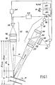
- the device comprises a transmitter assembly 10 and a receiver assembly 12, the whole positioned in a housing (not shown).
- the emitter assembly 10 comprises a light-emitting diode LED or a laser diode 14 and two focusing lenses 16 and 18. These two lenses make it possible to focus the radiation emitted by the laser diode at a distance D O from the lens 18.
- the convergent beam focused by the lenses 16 and 18 can be finish a focusing distance D of approximately 150 mm for a convergence angle of approximately 10 °.
- the transmitter 14 is chosen according to the application concerned. For example, it emits infrared radiation between 830 and 850 nm.
- the receiver assembly 12 comprises a lens 20, an interference filter 22, a semi-transparent plate 24, two lenses 26 and 28 and two detectors 30 and 32.
- the detectors 30 and 32 are photovoltaic detectors delivering a voltage signal proportional to the light flux which touches them.
- the lenses 26 and 28 associated respectively with the detectors 30 and 32 have different focal lengths.
- the focal lengths of the lenses 18 and 20 can be identical.
- the optical axes defined by the transmitter assembly 10 and by the receiver assembly 12 form between them an angle a whose influence on the value of the light flux received by each of the detectors will be seen later.
- the amplitude of the light beam delivered by the transmitter 14 is modulated by a circuit 34 at a given constant frequency, for example 40 kHz.
- the electrical signals delivered by each of the detectors 30 and 32 are demodulated in suitable circuits designated respectively by the references 36 and 38.
- the demodulation frequency of the signals delivered by the detectors is the same as the modulation frequency of the incident beam. It is provided by the modulator 34. In the encrypted example given above, this frequency is 40 kHz.
- the interference filter 22 is centered on the wavelength of the radiation emitted by the emitter 14.
- the immunity of the proximity measurement device according to the invention to ambient radiation is particularly important in the application of such a device to the reading of the profile of a surface in a welding robot.
- the signals D l and D 2 delivered by each of the sensors 30 and 32 and demodulated by the circuits 36 and 38 are injected into a processing circuit 40 which determines the ratio g between these signals.
- this ratio g depends only on the distance d which separates a reference point of the device, such as the lens 18, from the surface S of the part P.
- This signal V which varies linearly with the distance d, can be used directly or be used to control a control according to the envisaged application.
- a control circuit 44 is provided between the transmitter 14 and one of the detectors.
- this detector is the detector 32.
- the circuit 44 makes it possible to control the amplitude of the control signal from the transmitter 14, so that the flux received by the detector 32 remains constant whatever the Working conditions.
- the emitter assembly 10 projects a light spot on the surface S of this part.
- the incident beam is reflected on this surface, on which there is generally also a scattering of the projected radiation.
- Part of the beam returned by the surface S of the part P reaches the detectors 30 and 32 through the different optical components of the receiver assembly 12. Since the focal lengths of the lenses 26 and 28 are different, the bright spots in the detectors have a different diameter, so the detectors receive different light fluxes.
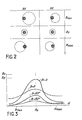
- the positions of the surfaces of the light spots formed at the level of each of the detectors 30 and 32 relative to the sensitive surface S d of the latter are represented in the form of a table, for three different positions of the surface S relative to the device.
- the constant sensitive surface S d of each of the detectors 30 and 32 has been represented by a small hatched circle.
- the areas of the light spots at the level of the detectors are the areas delimited by the large unshaded circles.
- the measurement range C is defined between the values D min and D max of the distance d, these values being themselves defined in an approximate and practical manner, and not rigorous.
- the invention is not limited to the simultaneous use of these two phenomena in the same device and also relates to comparable devices using only one of these phenomena.
- the device according to the invention can be made so that the incident beam and the beam returned by the surface have coincident optical axes.
- This result can be obtained for example, using semi-reflective plates by implementing techniques well known to opticians.
- the semi-reflecting plates divide by four the level of useful light energy compared to the level of the signal emitted by the source and that parasitic radiations appearing by reflection and by diffusion at the level of the plate reflecting the incident beam towards the surface can deteriorate the signal to noise ratio.
- the first phenomenon mentioned above comes into play.
- the device according to the invention therefore comprises a transmitter assembly emitting a parallel incident beam. This result can be easily obtained by an optician using appropriate optics.
- this embodiment also includes two variants.
- the incident and returned beams have coincident optical axes.
- the optical axes of the two beams are angularly offset.
- the device according to the invention therefore makes it possible to carry out a contactless measurement of the distance d.
- interference filter 22 as well as the modulation 34 and demodulation circuits 36 and 38 make it possible to immunize the device to ambient radiation, they are not essential to the invention and can be eliminated in certain particular applications in which this radiation is negligible.
- the servo circuit 44 can be eliminated in a simplified device.
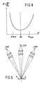
- FIG. 5 is essentially distinguished from the embodiment of FIG. 1 by the arrangement of the detectors.
- the two detectors 130 and 132 are arranged symmetrically with respect to the optical axis of the incident beam emitted by the emitter 114.
- the electronic part of the device which may be identical to that of the embodiment of FIG. 1, has not been shown.
- the signals delivered by the detectors are comparable to those which are delivered by the detectors 30 and 32 in the embodiment of FIG. 1, provided that the normal to the surface S of the part P is located in a plane containing the optical axis of the emitter 114 and perpendicular to the defined plane by the optical axes of the transmitter and detectors.
- This embodiment has the advantage of being sensitive to the surface state of the part, at the level of the light spot, and can deliver information on the roughness or the local reflection coefficient. This information is obtained by processing the AC component of the measurement signal, the DC component remaining a function of the distance.
- FIGs 6a and 6b there is shown schematically and by way of nonlimiting example a particularly interesting application of the device 'according to the invention to the survey of the profile of a surface, in association with a welding robot.
- the reference 350 designates the head of a welding robot supporting a welding torch 352.
- the head 350 comprises an axis 354 positioned above the surface of the parts P i and P 2 to be welded, so as to be substantially parallel to the joint line L formed between these parts, with the vertical of the welding torch 352.
- the axis 354 pivotally supports the housing 356 of the proximity measuring device according to the invention.
- FIGS. 6a and 6b show by way of example the case where this device is that which has been described with reference to FIG. 1. In fact, the transmitter assembly 10 and the receiver assembly 12 are recognized.
- the device 356 is supported by the axis 354, so that the incident beam strikes the parts P 1 and P 2 in front of the welding torch 352, as shown in FIG. 6b.
- Means such as an electric, hydraulic, pneumatic motor, etc. oscillate the device 356 about the axis 354, so that the incident and returned beams scan the profile of the welding zone slightly in front of the torch.
- This displacement corresponds to an angle 2e approximately centered with respect to the vertical plane passing through the joint line L.
- the voltage V delivered by the proximity measurement device being representative of the distance d, its evolution during the displacement along the angle 29 represents the profile of the surfaces of the parts P1 and P 2 on either side of the line L.
- the scanning of the surface using the proximity measurement device is carried out by different means.
- These means include guide rails allowing linear movement of the housing transversely to the joint and means such as a motor or an actuator for controlling this movement. An angular scan is thus replaced by a linear scan.
- the mechanical scanning obtained using the mechanism shown diagrammatically in FIGS. 6a and 6b is replaced by an optical scanning using known means for deflecting the light beam.
- Such optical scanning achieves higher frequencies than mechanical scanning.
- the information delivered by such a device makes it possible, using appropriate computer processing, to correct the trajectory of the welding torch during welding, to control the parameters such as the quantity during welding. of material to be provided during a pass, to raise the section to be filled, or even to position the welding passes relative to one another during multi-pass welding.
- this application is not limiting.
- the proximity measurement device according to the invention for carrying out the dimensional control of a part during manufacture. As soon as the distance leaves a tolerance interval defined in advance, the device according to the invention detects it. Automatic rejection of defective parts can therefore be carried out.
Landscapes
- Physics & Mathematics (AREA)
- General Physics & Mathematics (AREA)
- Engineering & Computer Science (AREA)
- Optics & Photonics (AREA)
- Geometry (AREA)
- Plasma & Fusion (AREA)
- Mechanical Engineering (AREA)
- Length Measuring Devices By Optical Means (AREA)
- Measurement Of Optical Distance (AREA)
Applications Claiming Priority (2)
| Application Number | Priority Date | Filing Date | Title |
|---|---|---|---|
| FR8403168 | 1984-02-29 | ||
| FR8403168A FR2560377B1 (fr) | 1984-02-29 | 1984-02-29 | Dispositif optique de mesure de proximite de surface et son application au releve du profil d'une surface |
Publications (2)
| Publication Number | Publication Date |
|---|---|
| EP0159210A1 true EP0159210A1 (de) | 1985-10-23 |
| EP0159210B1 EP0159210B1 (de) | 1989-05-24 |
Family
ID=9301555
Family Applications (1)
| Application Number | Title | Priority Date | Filing Date |
|---|---|---|---|
| EP85400334A Expired EP0159210B1 (de) | 1984-02-29 | 1985-02-22 | Optische Vorrichtung zum Messen der Annäherung an einer Fläche und Verfahren zum Wiedergewinnen des Profils einer solchen Fläche |
Country Status (5)
| Country | Link |
|---|---|
| US (1) | US4639140A (de) |
| EP (1) | EP0159210B1 (de) |
| JP (1) | JPS60205212A (de) |
| DE (1) | DE3570520D1 (de) |
| FR (1) | FR2560377B1 (de) |
Cited By (1)
| Publication number | Priority date | Publication date | Assignee | Title |
|---|---|---|---|---|
| GB2221533A (en) * | 1988-08-02 | 1990-02-07 | Oliver Engineering Limited | Probe positioning method and apparatus |
Families Citing this family (34)
| Publication number | Priority date | Publication date | Assignee | Title |
|---|---|---|---|---|
| US5162642A (en) * | 1985-11-18 | 1992-11-10 | Canon Kabushiki Kaisha | Device for detecting the position of a surface |
| GB2504248B (en) * | 1986-02-02 | 2014-07-23 | Selex Sensors & Airborne Sys | Imaging arrangement |
| US4743770A (en) * | 1986-09-22 | 1988-05-10 | Mitutoyo Mfg. Co., Ltd. | Profile-measuring light probe using a change in reflection factor in the proximity of a critical angle of light |
| GB8624191D0 (en) * | 1986-10-08 | 1986-11-12 | Renishaw Plc | Datuming of analogue measurement probes |
| US4786815A (en) * | 1987-02-12 | 1988-11-22 | K. J. Law Engineers, Inc. | Non-contact sensor with particular utility for measurement of road profile |
| FR2616223B1 (fr) * | 1987-06-03 | 1992-04-03 | Quartz & Silice | Procede et dispositif de controle du remplissage d'un moule par une matiere refractaire pulverulente |
| DE3743363A1 (de) * | 1987-12-21 | 1989-07-06 | Zeiss Carl Fa | Verfahren und einrichtung zur regelung der emissionslichtmenge in einem optischen tastkopf |
| US4896343A (en) * | 1988-05-02 | 1990-01-23 | Saunders Allan M | Radiation apparatus with distance mapper for dose control |
| US4888490A (en) * | 1988-05-24 | 1989-12-19 | University Of Southern California | Optical proximity apparatus and method using light sources being modulated at different frequencies |
| US4979815A (en) * | 1989-02-17 | 1990-12-25 | Tsikos Constantine J | Laser range imaging system based on projective geometry |
| US4933541A (en) * | 1989-06-29 | 1990-06-12 | Canadian Patents And Development Ltd. - Societe Canadienne Des Brevets Et D'exploitation Limitee | Method and apparatus for active vision image enhancement with wavelength matching |
| EP0419082B1 (de) * | 1989-09-21 | 1996-04-17 | Stanley Electric Corporation | Gerät zur optischen Abstandmessung |
| JPH03190652A (ja) * | 1989-12-19 | 1991-08-20 | Fanuc Ltd | 非接触ならい制御装置 |
| DE4039318A1 (de) * | 1990-12-10 | 1992-06-11 | Krupp Gmbh | Einrichtung zur erfassung der hoehenlage einer laserbearbeitungsvorrichtung bezueglich eines werkstuecks |
| JP2943499B2 (ja) * | 1992-04-22 | 1999-08-30 | 日本電気株式会社 | 高さ測定方法および装置 |
| US5870199A (en) * | 1992-09-02 | 1999-02-09 | Betriebsforschungsinstitut Vdeh Institut Fur Angewandte Forschung Gmbh | Method and apparatus for highly accurate distance measurement with respect to surfaces |
| US5298966A (en) * | 1992-11-10 | 1994-03-29 | Advanced Micro Devices, Inc. | Measurement system |
| JPH095048A (ja) * | 1995-06-16 | 1997-01-10 | Sony Corp | 表面形状測定装置 |
| US5801817A (en) * | 1997-05-05 | 1998-09-01 | Umm Electronics Inc. | Method and apparatus for eliminating the effects of varying sample distance on optical measurements |
| DE19855478B4 (de) * | 1998-12-01 | 2006-01-12 | Steinbichler Optotechnik Gmbh | Verfahren und Vorrichtung zur optischen Erfassung einer Kontrastlinie |
| US6441908B1 (en) * | 1999-08-06 | 2002-08-27 | Metron Systems, Inc. | Profiling of a component having reduced sensitivity to anomalous off-axis reflections |
| JP2001201324A (ja) * | 2000-01-20 | 2001-07-27 | Minolta Co Ltd | 形状計測装置 |
| US6572444B1 (en) | 2000-08-31 | 2003-06-03 | Micron Technology, Inc. | Apparatus and methods of automated wafer-grinding using grinding surface position monitoring |
| WO2004029540A2 (en) | 2002-09-26 | 2004-04-08 | Metron Systems, Inc. | Determination of the angular position of a laser beam |
| US6940891B2 (en) * | 2002-10-28 | 2005-09-06 | Metron Systems, Inc. | High precision optical imaging systems and related systems |
| AU2003285098A1 (en) * | 2002-10-29 | 2004-05-25 | Metron Systems, Inc. | Calibration for 3d measurement system |
| NO320062B1 (no) * | 2003-11-19 | 2005-10-17 | New Interaction Devices And Te | Anordning til a detektere naerhet mellom et forste objekt (malobjekt) og et annet objekt (referanseobjekt), samt tegne-, skrive- og/eller pekeredskap for datapresentasjon etc. |
| CA2620948A1 (en) * | 2005-09-02 | 2007-03-08 | Neptec | Apparatus and method for tracking an object |
| US20090195790A1 (en) * | 2005-09-02 | 2009-08-06 | Neptec | Imaging system and method |
| US7397540B2 (en) * | 2006-08-21 | 2008-07-08 | The Boeing Company | Phase diversity ranging sensor |
| JP2008082874A (ja) * | 2006-09-27 | 2008-04-10 | Fujitsu Ltd | 測定装置および測定方法 |
| US7684053B2 (en) * | 2006-12-12 | 2010-03-23 | Hong Kong Applied Science And Technology Research Institute Co., Ltd. | Optical displacement sensor and distance measuring apparatus |
| JP2014232005A (ja) * | 2013-05-28 | 2014-12-11 | 富士ゼロックス株式会社 | 計測装置 |
| ES2603650B1 (es) * | 2015-07-30 | 2017-09-05 | Abengoa Solar New Technologies, S.A. | Dispositivo y sistema de medida óptica del coeficiente de reflexión de una superficie |
Citations (7)
| Publication number | Priority date | Publication date | Assignee | Title |
|---|---|---|---|---|
| US3719421A (en) * | 1970-12-10 | 1973-03-06 | Compteurs Comp D | Optical device for determining the position of a point on a surface |
| US3885872A (en) * | 1973-06-12 | 1975-05-27 | Ibm | Digital proximity sensing system |
| US3986774A (en) * | 1975-05-08 | 1976-10-19 | United Technologies Corporation | Gauging surfaces by remotely tracking multiple images |
| US4088408A (en) * | 1976-11-08 | 1978-05-09 | The United States Of America As Represented By The Administrator Of The National Aeronautics And Space Administration | Device for measuring the contour of a surface |
| US4298286A (en) * | 1980-06-02 | 1981-11-03 | The Carl Maxey Company | Measuring apparatus |
| DE3110073A1 (de) * | 1981-03-16 | 1982-09-30 | Siemens AG, 1000 Berlin und 8000 München | Einrichtung zur weg-, geschwindigkeits- und/oder abstandsmessung |
| US4355904A (en) * | 1978-09-25 | 1982-10-26 | Balasubramanian N | Optical inspection device for measuring depthwise variations from a focal plane |
Family Cites Families (4)
| Publication number | Priority date | Publication date | Assignee | Title |
|---|---|---|---|---|
| SU868341A1 (ru) * | 1980-01-31 | 1981-09-30 | Завод-Втуз При Московском Трижды Ордена Ленина,Ордена Октябрьской Революции И Ордена Трудового Красного Знамени Автомобильном Заводе Им. И.А.Лихачева | Устройство дл бесконтактного измерени рассто ний |
| EP0071667A1 (de) * | 1981-08-11 | 1983-02-16 | Karl-Erik Morander | Vorrichtung zur Bestimmung des reellen oder virtuellen Abstands einer Lichtquelle von einer Messebene |
| JPS58111708A (ja) * | 1981-12-25 | 1983-07-02 | Sumitomo Metal Ind Ltd | 平担度測定装置 |
| ATE29698T1 (de) * | 1982-04-28 | 1987-10-15 | Ase Uk Ltd | Verstellbare fahrzeugsicherheitsgurtbefestigung. |
-
1984
- 1984-02-29 FR FR8403168A patent/FR2560377B1/fr not_active Expired
-
1985
- 1985-02-22 DE DE8585400334T patent/DE3570520D1/de not_active Expired
- 1985-02-22 EP EP85400334A patent/EP0159210B1/de not_active Expired
- 1985-02-26 US US06/705,734 patent/US4639140A/en not_active Expired - Fee Related
- 1985-02-28 JP JP60040259A patent/JPS60205212A/ja active Pending
Patent Citations (7)
| Publication number | Priority date | Publication date | Assignee | Title |
|---|---|---|---|---|
| US3719421A (en) * | 1970-12-10 | 1973-03-06 | Compteurs Comp D | Optical device for determining the position of a point on a surface |
| US3885872A (en) * | 1973-06-12 | 1975-05-27 | Ibm | Digital proximity sensing system |
| US3986774A (en) * | 1975-05-08 | 1976-10-19 | United Technologies Corporation | Gauging surfaces by remotely tracking multiple images |
| US4088408A (en) * | 1976-11-08 | 1978-05-09 | The United States Of America As Represented By The Administrator Of The National Aeronautics And Space Administration | Device for measuring the contour of a surface |
| US4355904A (en) * | 1978-09-25 | 1982-10-26 | Balasubramanian N | Optical inspection device for measuring depthwise variations from a focal plane |
| US4298286A (en) * | 1980-06-02 | 1981-11-03 | The Carl Maxey Company | Measuring apparatus |
| DE3110073A1 (de) * | 1981-03-16 | 1982-09-30 | Siemens AG, 1000 Berlin und 8000 München | Einrichtung zur weg-, geschwindigkeits- und/oder abstandsmessung |
Cited By (1)
| Publication number | Priority date | Publication date | Assignee | Title |
|---|---|---|---|---|
| GB2221533A (en) * | 1988-08-02 | 1990-02-07 | Oliver Engineering Limited | Probe positioning method and apparatus |
Also Published As
| Publication number | Publication date |
|---|---|
| US4639140A (en) | 1987-01-27 |
| FR2560377A1 (fr) | 1985-08-30 |
| EP0159210B1 (de) | 1989-05-24 |
| FR2560377B1 (fr) | 1988-05-13 |
| DE3570520D1 (en) | 1989-06-29 |
| JPS60205212A (ja) | 1985-10-16 |
Similar Documents
| Publication | Publication Date | Title |
|---|---|---|
| EP0159210B1 (de) | Optische Vorrichtung zum Messen der Annäherung an einer Fläche und Verfahren zum Wiedergewinnen des Profils einer solchen Fläche | |
| EP1209441B1 (de) | Messinstrument für 3D-Form mit Laserscanner | |
| EP0224437B1 (de) | Optische Vorrichtung mit Lichtbündel zur automatischen Kontrolle der Biegeoperation beim Biegen mit einer Abkantpresse | |
| EP0063980B1 (de) | Projektionsapparat mit einer Anordnung zum Scharfeinstellen | |
| CA1301319C (fr) | Dispositif de lecture optique de support d'enregistrement optique | |
| FR2539883A1 (fr) | Dispositif optique de focalisation pour la lecture d'un support d'informations defilant devant lui | |
| FR2534017A1 (fr) | Procede et appareil pour realiser l'alignement statique d'arbres et pour controler cet alignement | |
| FR2652166A1 (fr) | Dispositif d'harmonisation automatique pour un systeme optronique. | |
| FR2495338A1 (fr) | Dispositif pour la focalisation optique precise du rayonnement d'une source sur un objet | |
| EP0423295A1 (de) | Optische leseeinrichtung für einen optischen aufzeichnungsträger. | |
| CH658312A5 (fr) | Sonde optique astigmatique sans contact. | |
| EP0022682A1 (de) | Optischer Lesekopf mit Halbleiter-Laserquelle und eine mit optischer Reflexion arbeitende Lesevorrichtung zum Lesen eines Informationsträgers, die einen solchen optischen Lesekopf enthält | |
| EP0077693A1 (de) | Opto-elektronische Vorrichtung zum Auslesen der Information eines magnetischen Aufzeichnungsträgers | |
| EP0035423B1 (de) | Vorrichtung zur Detektion und Lokalisation von Oberflächendiskontinuitäten mit einem Lichtbündel | |
| EP0402191A1 (de) | Verfahren und Vorrichtung zum Messen der Linienbreite mit optischem Abtasten | |
| FR2620537A1 (fr) | Dispositif optique a mise au point automatique et appareil optique comportant un tel dispositif | |
| FR2668261A1 (fr) | Capteur optique avec moyens de pointage. | |
| FR2541029A1 (fr) | Appareil de lecture optique d'informations | |
| FR2489574A1 (fr) | Systeme opto-electronique de detection de mise au point et de reglage exact de piste | |
| FR2753533A1 (fr) | Procede et dispositif de caracterisation d'une modification au cours du temps de l'etat de condensation de gouttelettes sur une cible | |
| FR2618893A1 (fr) | Perfectionnements apportes aux appareils de reconnaissance de forme et/ou de detection de position d'un objet dans l'espace | |
| FR2558250A1 (fr) | Procede et dispositif de visualisation de discontinuites de surface et application de ce procede au soudage automatique de deux pieces | |
| CH629299A5 (fr) | Dispositif pour determiner la qualite du poli des surfaces optiques. | |
| FR2528570A1 (fr) | Procede optique permettant la reconnaissance precise et la restitution d'un profil localise et utilisable pour le pilotage automatique des machines-outils | |
| FR2661542A1 (fr) | Appareil optique de lecture de donnees sur un disque. |
Legal Events
| Date | Code | Title | Description |
|---|---|---|---|
| PUAI | Public reference made under article 153(3) epc to a published international application that has entered the european phase |
Free format text: ORIGINAL CODE: 0009012 |
|
| AK | Designated contracting states |
Designated state(s): CH DE GB IT LI SE |
|
| 17P | Request for examination filed |
Effective date: 19860307 |
|
| RAP1 | Party data changed (applicant data changed or rights of an application transferred) |
Owner name: COMMISSARIAT A L'ENERGIE ATOMIQUE |
|
| 17Q | First examination report despatched |
Effective date: 19880205 |
|
| GRAA | (expected) grant |
Free format text: ORIGINAL CODE: 0009210 |
|
| AK | Designated contracting states |
Kind code of ref document: B1 Designated state(s): CH DE GB IT LI SE |
|
| REF | Corresponds to: |
Ref document number: 3570520 Country of ref document: DE Date of ref document: 19890629 |
|
| ITF | It: translation for a ep patent filed | ||
| GBT | Gb: translation of ep patent filed (gb section 77(6)(a)/1977) | ||
| PLBE | No opposition filed within time limit |
Free format text: ORIGINAL CODE: 0009261 |
|
| STAA | Information on the status of an ep patent application or granted ep patent |
Free format text: STATUS: NO OPPOSITION FILED WITHIN TIME LIMIT |
|
| 26N | No opposition filed | ||
| PGFP | Annual fee paid to national office [announced via postgrant information from national office to epo] |
Ref country code: DE Payment date: 19910124 Year of fee payment: 7 |
|
| PGFP | Annual fee paid to national office [announced via postgrant information from national office to epo] |
Ref country code: SE Payment date: 19910130 Year of fee payment: 7 |
|
| PGFP | Annual fee paid to national office [announced via postgrant information from national office to epo] |
Ref country code: CH Payment date: 19910213 Year of fee payment: 7 |
|
| PGFP | Annual fee paid to national office [announced via postgrant information from national office to epo] |
Ref country code: GB Payment date: 19910221 Year of fee payment: 7 |
|
| ITTA | It: last paid annual fee | ||
| PG25 | Lapsed in a contracting state [announced via postgrant information from national office to epo] |
Ref country code: GB Effective date: 19920222 |
|
| PG25 | Lapsed in a contracting state [announced via postgrant information from national office to epo] |
Ref country code: SE Effective date: 19920223 |
|
| PG25 | Lapsed in a contracting state [announced via postgrant information from national office to epo] |
Ref country code: LI Effective date: 19920229 Ref country code: CH Effective date: 19920229 |
|
| GBPC | Gb: european patent ceased through non-payment of renewal fee | ||
| REG | Reference to a national code |
Ref country code: CH Ref legal event code: PL |
|
| PG25 | Lapsed in a contracting state [announced via postgrant information from national office to epo] |
Ref country code: DE Effective date: 19921103 |
|
| EUG | Se: european patent has lapsed |
Ref document number: 85400334.0 Effective date: 19920904 |