EP0159757A2 - Amplificateur à excursion d'entrée couvrant la tension d'alimentation et transconductance réglée - Google Patents
Amplificateur à excursion d'entrée couvrant la tension d'alimentation et transconductance réglée Download PDFInfo
- Publication number
- EP0159757A2 EP0159757A2 EP85200578A EP85200578A EP0159757A2 EP 0159757 A2 EP0159757 A2 EP 0159757A2 EP 85200578 A EP85200578 A EP 85200578A EP 85200578 A EP85200578 A EP 85200578A EP 0159757 A2 EP0159757 A2 EP 0159757A2
- Authority
- EP
- European Patent Office
- Prior art keywords
- current
- supply
- amplifier
- common
- range
- Prior art date
- Legal status (The legal status is an assumption and is not a legal conclusion. Google has not performed a legal analysis and makes no representation as to the accuracy of the status listed.)
- Granted
Links
Images

Classifications
-
- H—ELECTRICITY
- H03—ELECTRONIC CIRCUITRY
- H03F—AMPLIFIERS
- H03F3/00—Amplifiers with only discharge tubes or only semiconductor devices as amplifying elements
- H03F3/45—Differential amplifiers
- H03F3/45071—Differential amplifiers with semiconductor devices only
- H03F3/45076—Differential amplifiers with semiconductor devices only characterised by the way of implementation of the active amplifying circuit in the differential amplifier
- H03F3/45179—Differential amplifiers with semiconductor devices only characterised by the way of implementation of the active amplifying circuit in the differential amplifier using MOSFET transistors as the active amplifying circuit
- H03F3/4521—Complementary long tailed pairs having parallel inputs and being supplied in parallel
- H03F3/45219—Folded cascode stages
-
- H—ELECTRICITY
- H03—ELECTRONIC CIRCUITRY
- H03F—AMPLIFIERS
- H03F3/00—Amplifiers with only discharge tubes or only semiconductor devices as amplifying elements
- H03F3/45—Differential amplifiers
- H03F3/45071—Differential amplifiers with semiconductor devices only
- H03F3/45076—Differential amplifiers with semiconductor devices only characterised by the way of implementation of the active amplifying circuit in the differential amplifier
- H03F3/4508—Differential amplifiers with semiconductor devices only characterised by the way of implementation of the active amplifying circuit in the differential amplifier using bipolar transistors as the active amplifying circuit
- H03F3/45085—Long tailed pairs
-
- H—ELECTRICITY
- H03—ELECTRONIC CIRCUITRY
- H03F—AMPLIFIERS
- H03F3/00—Amplifiers with only discharge tubes or only semiconductor devices as amplifying elements
- H03F3/45—Differential amplifiers
- H03F3/45071—Differential amplifiers with semiconductor devices only
- H03F3/45076—Differential amplifiers with semiconductor devices only characterised by the way of implementation of the active amplifying circuit in the differential amplifier
- H03F3/4508—Differential amplifiers with semiconductor devices only characterised by the way of implementation of the active amplifying circuit in the differential amplifier using bipolar transistors as the active amplifying circuit
- H03F3/45112—Complementary long tailed pairs having parallel inputs and being supplied in parallel
- H03F3/45121—Folded cascode stages
-
- H—ELECTRICITY
- H03—ELECTRONIC CIRCUITRY
- H03F—AMPLIFIERS
- H03F3/00—Amplifiers with only discharge tubes or only semiconductor devices as amplifying elements
- H03F3/45—Differential amplifiers
- H03F3/45071—Differential amplifiers with semiconductor devices only
- H03F3/45076—Differential amplifiers with semiconductor devices only characterised by the way of implementation of the active amplifying circuit in the differential amplifier
- H03F3/45179—Differential amplifiers with semiconductor devices only characterised by the way of implementation of the active amplifying circuit in the differential amplifier using MOSFET transistors as the active amplifying circuit
- H03F3/45183—Long tailed pairs
-
- H—ELECTRICITY
- H03—ELECTRONIC CIRCUITRY
- H03F—AMPLIFIERS
- H03F3/00—Amplifiers with only discharge tubes or only semiconductor devices as amplifying elements
- H03F3/45—Differential amplifiers
- H03F3/45071—Differential amplifiers with semiconductor devices only
- H03F3/45479—Differential amplifiers with semiconductor devices only characterised by the way of common mode signal rejection
- H03F3/45484—Differential amplifiers with semiconductor devices only characterised by the way of common mode signal rejection in differential amplifiers with bipolar transistors as the active amplifying circuit
- H03F3/45547—Differential amplifiers with semiconductor devices only characterised by the way of common mode signal rejection in differential amplifiers with bipolar transistors as the active amplifying circuit by using feedforward means
- H03F3/45551—Measuring at the input circuit of the differential amplifier
- H03F3/4556—Controlling the common emitter circuit of the differential amplifier
-
- H—ELECTRICITY
- H03—ELECTRONIC CIRCUITRY
- H03F—AMPLIFIERS
- H03F3/00—Amplifiers with only discharge tubes or only semiconductor devices as amplifying elements
- H03F3/45—Differential amplifiers
- H03F3/45071—Differential amplifiers with semiconductor devices only
- H03F3/45479—Differential amplifiers with semiconductor devices only characterised by the way of common mode signal rejection
- H03F3/45632—Differential amplifiers with semiconductor devices only characterised by the way of common mode signal rejection in differential amplifiers with FET transistors as the active amplifying circuit
- H03F3/45695—Differential amplifiers with semiconductor devices only characterised by the way of common mode signal rejection in differential amplifiers with FET transistors as the active amplifying circuit by using feedforward means
- H03F3/45699—Measuring at the input circuit of the differential amplifier
- H03F3/45708—Controlling the common source circuit of the differential amplifier
Definitions
- This invention relates generally to differential amplifiers suitable for operational amplifiers made in semiconductor integrated circuit form and especially to differential amplifiers employing pairs of transistors to achieve rail-to-rail input capability.
- this invention relates to an amplifier operable between first and second supply voltages which define a supply range consisting of (a) a first end range extending from the first supply voltage to a first specified voltage between the supply voltages, (b) a middle range extending from the first specified voltage to a second specified voltage between the first specified voltage and the second supply voltage, and (c) a second end range extending from the second specified voltage to the second supply voltage, the amplifier having: first differential means for amplifying a differential input signal by largely dividing a first operating current into first and second internal currents whose difference is representative of the input signal when its common-mode voltage varies across the middle and second ranges; second differential means for amplifying the input signal by largely dividing a second operating current into third and fourth internal currents whose difference is representative of the input signal when the common-mode voltage varies across the first
- op amp operational amplifier
- V CM range is extended to the full supply range by utilizing complementary pairs of input transistors.
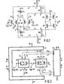
- Fig. 1 shows the known amplifier.
- This amplifier has a differential input section containing complementary differential portions 10 and 12 which amplify the differential input signal defined by voltages V I+ and V I- .
- Voltage V I+ is V CM + - V
- voltage V I- is V CM - ⁇ V ,where 2 ⁇ V is the differential part of the input signal.
- Current sources 14 and 16 respectively connected to points (or terminals) of low and high supply voltages V L and V B provide the supply current for the input section.
- circuit 18 is a modulated current mirror for combining signal currents from differential portions 10 and 12 to provide an output current I O .
- V PS -- The range for the power supply voltage V PS -- i.e., V H -V L -- is divided into three ranges.
- a low range goes from V L up to slightly more than V L +V BE , where V BE is the absolute value of the standard base-to-emitter voltage of a bipolar transistor when it is just turned on.
- a high range goes from V H down: to slightly less than V H -V BE . With V PS being greater than 2V BE , a middle range extends between the two end ranges.
- Differential portion 10 contains NPN transistors Q1 and Q2 which amplify the input signal by dividing operating current provided from current source 14 on interconnected lines SA and SB into respective currents I A and I B transmitted on lines LA and LB.
- the difference between currents IA and I D is representative of the input signal when V CM is in the middle and high ranges where the operating current is at a constant supply level I L . As V CM drops into thelow range, first one and then the other of transistors Q1 and Q2 turn off to shut down current source 14.
- differential portion 12 has PNP transistors Q3 and Q4 which divide operating current provided from current source 16 on interconnected lines SC and SD into respective currents I C and I D transmitted on lines LC and LD.
- the difference between current I C and I D is representative of the input signal when V CM is in the low and middle ranges where the operating current for transistors Q3 and Q4 is at a constant supply level I H . They turn off to shut down current source 16 when V CM goes into the high range. Accordingly, portions 10 and 12 are both active in the middle range, but only one is active in each end range.
- a measure of the amplification capability of a differential amplifier is its transconductance G MA (i.e., the ratio of the incremental change in total current through the input section to input voltage change ⁇ V).
- G MA for Fig. 1 is a approximately proportional to I A +I B +I C +I D .
- the total supply current transmitted by current sources 14 and 16 is the sum of the operating currents which, in turn, largely equals the sum of currents I A - I D . Since the current supply for the input section partly shuts down when V CM is in either end range, the total supply current is greater when V CM is in the middle range.
- the amplifier transconductance then varies in the same manner.
- an amplifier of the type set forth in the preamble is characterized in that the amplifier is provided with control means for providing amplifier supplyrcurrent to generate the operating currents and for steering at least part of the supply current away from at least one of the differential means when the common-mode voltage is in at least one part of the supply range so as to control the operating currents at values dependent on the steering of the supply current.
- an amplifier for amplifying a differential input signal has rail-to-rail input capability with a transconductance that can be controlled as the common-mode voltage of the input signal varies across the power supply range.
- the current control optimally maintains the sum of the operating currents largely constant as the common-mode voltage varies across the rail-to-rail range. This enables the amplifier transconductance to be largely constant. This facilitates optimization of the frequency response by enabling the loop gain to be largely constant when the amplifier is used with a negative feedback network and reduces signal distorsion in negative feedback applications.
- the basic technique involves diverting at least part of the supply current away from the supply lines for one of the differential portions as the common-mode voltage goes into the end range where the input transistors in that differential portion are non-conductive. This is preferably done with one or more steering transistors differentially configured with respect to one or both pairs of input transistors.
- the supply lines for the other differential portion are then provided with current derived from the current diverted away. As a result, the portion of the current control that provides the supply current normally does not partially shut down.
- the configuration of the amplifier is quite simple. It typically uses just a few more transistors than the prior are device described above. Consequently, the present amplifier is especially suited for use as an op amp input stage in low power supply applications.
- Fig. 2 shows a general differential amplifier having rail-to-rail input capability with controlled transconductance.
- This amplifier has a differential input section consisting of a pair of differential input portions 20 and 22 that commonly receive the differential input signal formed by voltages V j+ and V I- .
- a current control 24 responsive to one or both of control voltages V RN and V RP is connected between points for low and high supply voltages V L and V H .
- a summing circuit 26 connected between the V L and V H terminals provides one or more output current signals representative of the input signal.
- Differential portion 20 contains identical like-polarity input transistors Q1 and Q2, while differential portion 22 contains identical like-polarity input transistors Q3 and Q4.
- transistors Q1 - Q4 are shown as bipolar transistors, they may be field-effect transistors (FET's) of the insulated-gate or junction type.
- Transistors Q3 and Q4 are typically complementary to transistors Q1 and Q2, particularly if the amplifier is embodied in bipolar or CMOS technology.
- Transistors Q1 - Q4 may, however, all be of the same polarity in some circumstances. For example, transistors Q1 and Q2 could be depletion-mode FET's, while transistors Q3 and Q4 are enhancement-mode FET's.
- a transistor such as any of transistors Q1 - Q4 or the other transistors described below has a first flow electrode, a second flow electrode, and a control electrode for regulating current transmission between the flow electrodes.
- a bipolar transistor its base, emitter, and collector are respectively the control, first, and second electrodes. These are the gate, source, and drain for an FET.
- Transistors Q1 - Q4 are all turned on when V CM is in a middle range extending from a specified voltage greater than V L to a specified voltage less than V H .
- Transistors Q1 and Q2 are also conductive when V CM is in a high range extending from the top of the middle range to V M . They are non-conductive when V CM is in part or all of a low range extending from the bottom of the middle range to V L . The reverse is true for transistors Q3 and Q4. They are turned on in the low range but are turned off in part or all of the high range.
- transistors Q1 and Q2 Responsive to the input signal differentially supplied to their control electrodes, transistors Q1 and Q2 jointly control current flow between supply and internal lines SA and LA and between supply and internal lines SB and LB.
- Lines SA and SB are connected together to carry an operating current IN for portion 20. It amplifies the input signal by largely dividing operating current IN into internal currents I A and I B which are respectively transmitted on lines LA and LB and whose difference is representative of the input signal when V CM is is the middle and high ranges. For the low range, current IN is substantially zero so that portion 20 provides no signal amplification.
- transistors Q3 and Q4 Responsive to the input signal differentially supplied to their control electrodes, transistors Q3 and Q4 jointly control current flow between supply and internal lines SC and LC and between supply and internal lines SD and LD. Lines SC and SD are similarly connected together to carry an operating current Ip for portion 22. It amplifies the input signal by largely dividing operating current Ip into internal currents IC and I D which are respectively transmitted on lines LC and LD and whose difference is representative of the input signal when V CM is in the low and middle ranges. For the high range, current Ip is substantially zero so that portion 22 provides no signal amplification.
- the direction of current flow for currents I A and I B is indicated as being toward portion 20 in Fig. 2, whereas the flow direction for currents I c and I D is shown as being away from direction 22.
- the flow direction for currents I A and I B may, however, be opposite to that shown.
- the flow direction for current IN is also reversed from that shown.
- currents I C , I D and Ip Their flow directions with respect to portion 22 may all be reversed depending on its configuration.
- Summing circuit 26 receives the currents on internal lines LA-LD at respective nodes A, B, C and D and suitably combines these currents to generate one or more output currents.
- Complementary output currents I O+ and I O- may be provided if circuit 26 is a double-ended device as indicated in Fig. 2.
- Circuit 26 could also be a single-ended device (such as depicted in Fig. 1) that provides single output current I O .
- Current control 24 provides amplifier supply current that is utilized in generating operating currents I N and Ip for the differential input section.
- the supply current is substantially constant when V CM is in the rail-to-rail range.
- the portion of control 24 that provides the supply current normally does not partially shut down in any part of the V PS range.
- Control 24 which is connected to portion 20 by way of lines SA and SB and to portion 22 by way of lines SC and SD controls the transconductance of the amplifier by regulating operating currents I N and Ip.
- V CM When V CM is in at least one part of the Vp S range, control 24 steers at least part of supply current through itself and provides currents I n and Ip at values depending on the steering of the supply current.
- control 24 operates by steering supply current away from one of portions 20 and 22 as V CM goes into the end range where the input transistors of that differential portion turn off and provides the other of portions 20 and 22 with current derived from the current steered away. This steering may be done with either or both of portions 20 and 22.
- the discussion below of particular embodiments of the amplifier of Fig. 2 further clarifies the steering mechanism.
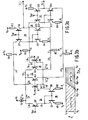
- Fig. 3a shows an embodiment of Fig. 2 in which transistors Q1 and Q2 are NPN transistors whose bases receive the input signal, whose emitters are respectively connected to lines SA and SB to receive current I N , and whose collectors are respectively connected to lines LA and LB to provide currents I A and I B .
- Transistors Q3 and Q4 are PNP transistors whose bases receive the input signal, whose emitters are respectively connected to lines SC and SD to receive current Ip, and whose collectors are respectively connected to lines LC and LD to provide current I C and I D .
- Control 24 in Fig. 3a consists of current source 16 that provides the amplifier supply current at constant level IH, a current mirror 28, and a PNP steering transistor QP.
- Reference voltage V RP is supplied to the base of transistor QP. Its emitter is connected to a steering line LH connected in common with lines SC and SD to current source 16. This places transistor QP in a differential configuration with transistors Q3 and Q4.
- Mirror 28 contains identical NPN transistors Q5 and Q6 whose bases are connected to the Q5 collector which is connected through a steering line LN to the QP collector.
- the Q6 collector is connected to lines SA and SB.
- the emitters of transistors Q5 and Q6 are coupled through respective equal-valued resistors R1 and R2 to the V L terminal. Resistors R1 and R2 reduce sensitivity to noise.
- transistor QP The current flow through transistor QP is in the wrong direction for providing current by way of lines SA and SB to transistors Q1 and Q2.
- Mirror 28 largely mirrors (duplicates) the current on line LN at the Q5 collector and provides the mirrored current at the Q6 collector in the right direction for transistors Q1 and Q2.
- Fig. 3b shows a graph helpful in understanding the operation of control 24 in Fig. 3a.
- Voltage V RP is at a selected value within the range extending from V L +V BE +V SM to Y H- V BE- V SM where V SM is a small safety-margin voltage typically about 0.2 - 0.3 volt.
- Vp S must be at least 2V BE +2V SM .
- V BE is about 0.6 - 0.8 volt.
- the middle range where transistors Q1 - Q£ are all conductive is an approximate 50-millivolt range centering on voltage V RP . This is the case when the QP emitter area equals the sum of the emitter areas of transistors Q3 and Q4.
- V W (which equals 50 millivolts) be the width of the middle range, it extends from V RP -V W to V RP +V W .
- trans is- tor QP switches from substantially fully off to fully on, while transistors Q3 and Q4 do the opposite.
- base currents are ignored in comparison to collector or emitter currents.
- indicated equalities mean that items indicated as being equal are only largely equal.
- the various graphs only show asymptotes for the variation of currents I N and Ip. The rounding that occurs at the ends of the middle ranges is generally not shown in these graphs.
- transistor QP In the low V CM range where transistors Q3 and Q4 are turned on, transistor QP is off since its emitter-base voltage is less than V BE -V W .
- Current source 16 supplies current Ip to portion 22 at level I H .
- the sum of currents I C and I D is thereby I H .
- Transistors Q5 and Q6 are off because transistor QP is off. Since current IN is thereby zero, transistors Q1 and Q2 are off.
- transistor QP turns on and progressively becomes more conductive. It steers a progressively increasing part of current I H away from transistors Q3 and Q4, causing them to become progressively less conductive as current Ip progressively decreases toward zero.
- the I H part steered away from portion 22 is transmitted through transistor QP to transistor Q5 so as to turn on transistors Q5 and Q6.
- Mirror 28 duplicates this In part and provides the duplicated current portion by way of lines SA and SB to transistors Q1 and Q2 which progressively turn on. Current IN which equals the duplicated I H part progressively increases towards level I H .
- the sum of currents I A - I D is Ip + IN which equals the constant supply current I H across the entire rail-to-rail range for V CM .
- the transconductance G MA of the amplifier of Fig. 3a is approximately (I A +I B +I O +I D )/V T which equals I H /V T .
- V T is kT/q where T is temperature, k is Boltzmann's constant, and q is the electronic charge.
- G MA is largely constant across the V PS range.
- Summing circuit 26 in Fig. 3a contains a modulated current mirror 30 consisting of transistors Q7, Q8, Q9, and Q10, an identical modulated current mirror 32 consisting of transistors Q11, Q12, Q13, and Q14, and equal-valued resistors RA - RD and R3, R4, R5, and R6 connected as shown to provide complementary currents I O+ and I O- .
- the bases of transistors Q7, Q8, Q11 and Q12 receive bias voltage VBp.
- Mirrors 30 and 32 operate in the manner described in U.S. Patent Application Ser. No. 525,181, cited above, except that transistors Q8, Q9, Q12, and Q13 do not receive signal inputs.
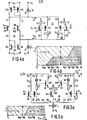
- Fig. 4a depicts a partial embodiment of the present amplifier in which portions 20 and 22 are configured the same as in Fig. 3a.
- the principal difference is in current control 24 where current sources 14 and 16 provide supply currents at constant levels I L and I H .
- the amplifier supply current for the differential input section is the sum of I L and I H .
- a summing circuit (not shown in Fig. 4a) is connected to nodes A-D of the input section to generate the output current(s).
- Control 24 in Fig. 4a contains transistor QP and mirror 28 configured the same as in Fig. 3a except that anti-noise resistors R1 and R2 are omitted in Fig. 4a.
- Control 24 further includes a current mirror 34 and an NPN steering transistor QN.
- Reference voltage V RN is supplied to the base of transistor QN. Its emitter is connected to steering line LL connected in common with lines SA and SB to current source 14. This places transistor QN in a differential configuration with transistors Q1 and Q2.
- Mirror 34 contains identical PNP transistors Q15 and Q16 whose bases are connected to the Q15 collector which is connected through a steering line LP to the QN collector.
- the Q16 collector is connected to lines SC and SD.
- the emitters of transistors Q15 and Q16 are tied to the V H terminal.
- Fig. 4b shows a graph that facilitates understanding the operation of control 24 in Fig. 4a.
- Voltages V RP and V RN are both at selected values within the ranga extending from V L +V BE +V SM to V H -B E -V sm .
- V RN is less than V RP -2V W .
- V PS is again at least 2V BE +2V SM .
- the middle range extends from V RN -V W up to V RP +V W .
- transistor Qn switches from fully on to substantially fully off while transistors Q1 and Q2 do the opposite.
- the QP emitter-base voltage rises from V BE -V W to V BE +V W (at the upper portion of the middle range)
- transistor QP switches from substantially fully off to fully on while transistors Q3 and Q4 do the reverse.
- transistors Q1 and Q2 are off so that current I N is zero.
- Transistor QN is on and steers current I L away from portion 20 to transistor Q15 so as to turn on transistors Q15 and Q16.
- Mirror 34 duplicates current I L at the Q15 collector and provides the duplicated current from the Q16 collector to portion 22.
- Transistors Q5 and Q6 are off since transistor QP is off.
- Current source 16 then provides current I H directly to portion 22. As a result, current Ip equals I L +I H .
- transistor QN becomes progressively less conductive and steers a progressively decreasing part of current I L away from transistors Q1 and Q2.
- Mirror 34 duplicates the I L part steered away from portion 20 and supplies the duplicated current to portion 22 so that current Ip progressively decreases toward I H .
- current source 14 provides a progressively increasing part of current I L to transistors Q1 and Q2, causing them to turn on and become progressively more conductive.
- Current IN progressively increases toward I L .
- transistors QN and QP are both off. Mirrors 28 and 34 are therefore both off. No steering occurs.
- Current source 14 provides current IN to portion 20 at level I L .
- Current source 16 provides current Ip to portion 22 at level I H .
- transistor QN and mirror 28 operate on current I H in the same way that transistor QP and mirror 34 respectively operate on current I L in the lower middle-range portion and in the low range.
- current Ip decreases progressively toward zero and then stays there as V CM rises through the upper middle-range portion and the high range.
- Current IN increases progressively towards I L +I H and then stays there.
- the sum of currents I A - I D is constant at level I L +I H .
- the transconductance for Fig. 4 is therdbre constant when V CM varies across the rail-to-rail range.
- Fig. 5a shows an embodiment of the present amplifier in which portion 20 is configured the same as in Fig. 4a, but portion 22 is configured differently.
- Portion 22 in Fig. 5a contains a level shifter that translates the input signal into a shifted differential signal whose common-mode voltage is at least 1VBE closer to VH.
- the level shifter contains PNP transistors Q3 and Q4 whose bases differentially receive the input signal and whose collectors are connected to the VL supply pointo
- the emitters of transistors Q3 and Q4 are connected to the lower ends of respective resistors R7 and R8 whose upper ends provide the shifted differential signal and are respectively coupled through constant current sources 36 and 38 to the V B supply point.
- the shifted signal is differentially supplied to the bases of identical NPN transistors Q17 and Q18. Their collectors are respectively connected to lines LC and LD to provide currents I C and I D , and their emitters are respectively connected to lines SC and SD to carry current Ip.
- Control 24 in Fig. 5a consists of current source 14 and NPN steering transistor QN whose base receives voltage V RN .
- the QN collector is connected through line LP to lines SC and SD.
- the QN emitter is connected to line LL connected commonly with lines SA and SB to current source 14 so that transistor QN is in a differential configuration with transistors Q1 and Q2.
- Fig. 5b shows a graph helpful in understanding the operation of control 24 in Fig. 5a.
- Voltage V RN is at a selected value within the range extending from V L +V BE + V SM to V H -V BE -V SM .
- transistor QN is on along with transistors Q3 and Q4.
- the shifted signal is provided to transistors Q17 and Q18 which are also on.
- Transistor QN diverts current I L from current source 14 away from portion 20 to portion 22 to generate current Ip at level I L .
- transistor QN becomes progressively less conductive and does progressively less current steering, while transistors Q1 and Q2 turn on and become progressively more conductive.
- Current I N progressively increases from zero to I L .
- Current Ip does the reverse.
- transistor QN is off so that transistors Q17 and Q18 are off.
- Current source 14 supplies current IN to portion 20 at level I L . If V CM rises high enough, transistors Q3 and Q4 turn off. This, however, does not affect operation in the high range.
- Fig. 6 illustrates a preferred embodiment of the amplifier of Fig. 2 in which portions 20 and 22 and control 24 are configured as in Fig. 3a except that the input signal is supplied through resistors R9 and R10 to portions 20 and 22.
- Current source 16 consists of a PNP transistor QS and a resistor RS connected as shown.
- Summing circuit 26 in Fig. 6 contains PNP transistors QA and QB and NPN transistors QC and QD connected as shown in Fig. 1 except that the bases of transistors QC and QD receive a bias voltage V BN . This enables circuit 26 to provide output I O+ from the QB and QD collectors and output I O- from the QA and QC collectors.
- Circuit 26 in Fig. 6 operates as follows. As seen from line LA, resistor RA is a high impedance whereas transistor QA:is a low impedance. The same holds for lines LB - LD with respect to resistors RB - RD and transistors QB - QD. ; When incremental currents ⁇ I N , - ⁇ I N ' - Ip, and Ip occur respectively on lines LA - LD, opposite incremental currents respectively flow through transistors QA - QD. As a result, currents I O+ and I O- respectively equal IN + Ip and - I N - Ip. Since G MA which equals 2(I N + Ip)/ V is constant across the rail-to-rail range, currents I O+ and I O- are largely independent of the location of V CM in the V PS range.
- a set of Schottky diodes D1, D2, D3 and D4 in combination with resistors R9 and R10 prevents the polarities of outputs I O+ and I O- from inverting when V CM drops below V L or rises above V H . Typically, this protection occurs in ranges extending about 10 volts below V L and 10 volts above V H .
- Diodes D1 and D2 are cross coupled as shown between transistors Q3 and Q4.
- Diodes D3 and D4 are connected between current source 16 and respective resistors R9 and R10.
- Diodes D5 and D6 are connected in parallel in opposing directions between resistors R9 and R10.
- Each of diodes D5 and D6 is preferably an NPN transistor having its base connected to its collector.
- voltages V H and V L are preferably greater than 0.9 volt and less than -0.9 volt.
- Voltage V RP or V BN is 0.8 volt above V L
- voltage VBP is 0.8 volt below V H .
- Resistors R5/R6, R9/R10, RA/RB/RC/RD and RS are respectively 1,000, 3,000, 50,000 and 50,000 ohms.
- each pair of corresponding transistors such as transistors Q1 and Q2 may be replaced with a pair of groups of transistors arranged in identical voltage following configurations.
- Such a bipolar group typically consists of a lead transistor whose emitter is coupled directly or through one or more other transistors to the base of a trailing transistor. The input signal to the group is supplied to the base of the leading transistor to control current flow between lines connected to the emitter and collector of the trailing transistor.
- a pair of corresponding transistors in portion 20 or 22 is in a differential configuration with a steering transistor in control 24, that transistor may also be replaced with a group of transistors arranged in a corresponding voltage following configuration.
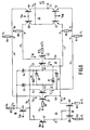
- Fig. 7 illustrates how this replacement can be done in the embodiment of Fig. 5a.
- transistor Q1 is replaced with a Darlington transistor pair in which the emitter of transistor Q1 is connected to the base of an NPN transistor Q21 whose emitter and collector are respectively connected to lines SA and LA. Voltage V I+ is still provided to the base of transistor Q1 but its collector is tied to the V H terminal.
- Transistor Q2 is replaced in the same manner with a Darlington pair consisting of transistor Q2 and an NPN transistor Q22 which is identical to transistor Q21.
- Transistors Q3, Q4, Q17, and Q18 are similarly replaced with Darlington pairs respectively consisting of transistor Q3 and a PNP transistor Q23, transistor Q4 and a PNP transistor Q24 identical to transistor Q23, transistor Q17 and an NPN transistor Q27, and transistor Q18 and an NPN transistor Q28 identical to transistor Q27. Since transistors Q1 and Q2 in Fig. 5a are in a differential configuration with transistor QN, it is normally replaced in the same manner with a Darlington pair consisting of transistor QN and an NPN transistor QN'.
- Vp S must be at least 4V BE +2V SM
- Voltage V RN is at a selected value within the range extending from V L +2V BE +V SM to V H -2V BE -Y SM ⁇
- voltage V RN could be reduced 1V BE instead of replacing transistor QN with a Darlington pair.
- the amplifier of Fig. 7 operates the same as described above for the amplifier of Fig. 5a.
- the present amplifier may be embodied partly or wholly with FET's.
- Fig. 8a depicts a partial embodiment similar to that of Fig. 4a but using CMOS technology. All the transistors in Fig. 8a are preferably enhancement-mode MOS FET's. Each N-channel FET is indicated by an arrow on its source pointing away from the FET. Each P-channel: FET is indicated by an arrow on its source pointing toward the FET.
- the input section in Fig. 8a contains portions 20 and 22 interconnected with control 24 in the same way as the corresponding items are interconnected in Fig. 4a.
- Mirror 28 of Fig. 4a is replaced with a reversing circuit 42 in which a resistor RN is connected between the Q5 source and the V L terminal.
- Circuit 42 provides the Q6 drain with current of greater magnitude than, but opposite flow direction to, the current through the Q5 drain.
- mirror 34 is replaced with a reversing circuit 44 in which a resistor RP is connected between the Q15 source and the V H supply point.
- Circuit 44 provides the Q16 drain with current of greater magnitude than, but opposite flow direction to, the current through the Q15 drain.
- the current amplifications in circuit 42 and 44 depend on the values of resistors RN and RP.
- Control 24 then consists of current sources 14 and 16, transistors QN and QP, and circuits 42 and 44.
- Fig. 8b shows a graph that facilitates understanding the operation of control 24 in Fig. 8a.
- the operation is generally the same as that of Fig. 4a.
- the V CM ranges are qualitatively the same.
- the width 2V W of the lower and upper middle range portions depends on the types of FET's used.
- the steering in the input section of Fig. 8a is the same as that in Fig. 4a except for the current amplifications provided by circuits 42 and 44.
- the sum of operating currents Ip and IN equals I L +I N . Because of the current amplification at the Q16 drain, the sum of currents Ip and I N progressively increases as V CM decreases from V RN +V W to V L .
- the current amplification at the Q16 drain causes the sum of currents Ip and I N to progressively increase as V CM increases from V RP +V W to V H . Consequently, the sum of currents I A - I D is greater when V CM is at V L or V H than when V CM is in the middle of the supply range.
- the transconductance for a MOS FET is -approximately proportional to the square root of its drain current. If circuits 42 and 44 were simply current mirrors that provided no current ampliflcation, G MA would decrease as V CM moves from the central portion of the middle range out to C L or V H . The current amplification provided at the Q6 and Q16 drains increases G MA in the parts of the V PS range outside the central portion of the middle range. The G MA variation as V CM moves across the Vp S range can be controlled upward by adjusting the amplifications of circuits 42 and 44. Suitable choice for their amplifications makes the amplifier transconductance relatively constant. As an example, GMA is largely constant if the amplifications of circuits 42 and 44 increase from 1 when they are just turned on to about 3 when they are fully conductive.
- circuits 42 and 44 can be configured to give current reduction rather than amplification. G MA would then decrease even more as V CM moves outward from the central portion of the middle range. Such a GMA variation might be desirable in some applications.
- the amplifier is preferably fabricated as part of a monolithic integrated circuit using PN-junction isolation to separate active regions in a semiconductor wafer.
Landscapes
- Engineering & Computer Science (AREA)
- Power Engineering (AREA)
- Amplifiers (AREA)
Applications Claiming Priority (2)
| Application Number | Priority Date | Filing Date | Title |
|---|---|---|---|
| US06/602,231 US4555673A (en) | 1984-04-19 | 1984-04-19 | Differential amplifier with rail-to-rail input capability and controlled transconductance |
| US602231 | 2000-06-23 |
Publications (3)
| Publication Number | Publication Date |
|---|---|
| EP0159757A2 true EP0159757A2 (fr) | 1985-10-30 |
| EP0159757A3 EP0159757A3 (en) | 1988-01-07 |
| EP0159757B1 EP0159757B1 (fr) | 1992-12-02 |
Family
ID=24410514
Family Applications (1)
| Application Number | Title | Priority Date | Filing Date |
|---|---|---|---|
| EP85200578A Expired EP0159757B1 (fr) | 1984-04-19 | 1985-04-16 | Amplificateur à excursion d'entrée couvrant la tension d'alimentation et transconductance réglée |
Country Status (5)
| Country | Link |
|---|---|
| US (1) | US4555673A (fr) |
| EP (1) | EP0159757B1 (fr) |
| JP (1) | JPH0680991B2 (fr) |
| CA (1) | CA1219045A (fr) |
| DE (1) | DE3586863T2 (fr) |
Cited By (8)
| Publication number | Priority date | Publication date | Assignee | Title |
|---|---|---|---|---|
| EP0259879A3 (en) * | 1986-09-10 | 1989-03-08 | Nec Corporation | Operational amplifier circuit having wide operating range |
| EP0318263A3 (en) * | 1987-11-24 | 1990-03-21 | Texas Instruments Incorporated | Folded cascode amplifier with rail-to-rail common-mode range |
| EP0416703A3 (en) * | 1989-09-08 | 1991-07-24 | N.V. Philips' Gloeilampenfabrieken | Rapid-response differential amplifier with rail-to-rail input capability |
| FR2672749A1 (fr) * | 1991-02-12 | 1992-08-14 | Sgs Thomson Microelectronics | Amplificateur operationnel a transconductance a grande excursion de mode commun. |
| EP0569102A3 (en) * | 1992-05-08 | 1994-07-06 | Koninkl Philips Electronics Nv | Differential amplifier having rail-to-rail input capability and square-root current control |
| EP0617508A1 (fr) * | 1993-03-25 | 1994-09-28 | Koninklijke Philips Electronics N.V. | Combinaison d'un circuit de commande et d'un circuit sommateur pour amplificateur différentiel avec une plage de signaux couvrant la tension d'alimentation |
| EP0595589A3 (fr) * | 1992-10-30 | 1994-10-12 | Sgs Thomson Microelectronics | Amplificateur différentiel ayant une sortie équilibrée et une plage de signaux d'entrée de mode commun couvrant la tension d'alimentation. |
| WO1997003496A1 (fr) * | 1995-07-07 | 1997-01-30 | Advanced Micro Devices, Inc. | Amplificateur operationnel cascode a plusieurs etages d'entree |
Families Citing this family (79)
| Publication number | Priority date | Publication date | Assignee | Title |
|---|---|---|---|---|
| JPH0618309B2 (ja) * | 1986-09-10 | 1994-03-09 | 日本電気株式会社 | 演算増幅回路 |
| US4978959A (en) * | 1987-10-08 | 1990-12-18 | University Of Toronto Innovations Foundation | Analog to digital converter, a digital to analog converter and an operational amplifier therefor |
| US4812781A (en) * | 1987-12-07 | 1989-03-14 | Silicon General, Inc. | Variable gain amplifier |
| JP2567278B2 (ja) * | 1989-01-25 | 1996-12-25 | ファナック株式会社 | 光学式エンコーダのオフセット調整方法 |
| US4918398A (en) * | 1989-02-10 | 1990-04-17 | North American Philips Corporation, Signetics Division | Differential amplifier using voltage level shifting to achieve rail-to-rail input capability at very low power supply voltage |
| KR960009739B1 (en) * | 1991-05-14 | 1996-07-23 | Toshiba Kk | Differential input circuit |
| JPH07130193A (ja) * | 1993-09-10 | 1995-05-19 | Toshiba Corp | バッファ回路及びこれを用いた液晶ディスプレイ装置 |
| US5455535A (en) * | 1994-03-03 | 1995-10-03 | National Semiconductor Corporation | Rail to rail operational amplifier intermediate stage |
| US5414388A (en) * | 1994-03-03 | 1995-05-09 | National Semiconductor Corporation | Rail to rail operational amplifier input stage |
| US5500624A (en) * | 1994-11-02 | 1996-03-19 | Motorola, Inc. | Input stage for CMOS operational amplifier and method thereof |
| US5717350A (en) * | 1994-11-09 | 1998-02-10 | Micro Linear Corporation | Degenerated differential pair waveform builder |
| US5550510A (en) * | 1994-12-27 | 1996-08-27 | Lucent Technologies Inc. | Constant transconductance CMOS amplifier input stage with rail-to-rail input common mode voltage range |
| US5561396A (en) * | 1995-04-27 | 1996-10-01 | Philips Electronics North America Corporation | Rail-to-rail input stages with gm -control by multiple input pairs |
| GB9516025D0 (en) * | 1995-08-04 | 1995-10-04 | Philips Electronics Uk Ltd | Amplifier |
| US5764101A (en) * | 1995-08-23 | 1998-06-09 | National Semiconductor Corporation | Rail-to-rail input common mode range differential amplifier that operates with very low rail-to-rail voltages |
| US5726592A (en) * | 1995-12-18 | 1998-03-10 | International Business Machines Corporation | Self biased low-voltage differential signal detector |
| US5734297A (en) * | 1996-03-29 | 1998-03-31 | Philips Electronics North America Corporation | Rail-to-rail input stages with constant gm and constant common-mode output currents |
| US5777514A (en) * | 1996-09-27 | 1998-07-07 | Micro Linear Corporation | Differential to single ended conversion technique for an operational amplifier having low input offset voltage, high speed and high gain |
| US5923129A (en) * | 1997-03-14 | 1999-07-13 | Linfinity Microelectronics | Apparatus and method for starting a fluorescent lamp |
| US5930121A (en) * | 1997-03-14 | 1999-07-27 | Linfinity Microelectronics | Direct drive backlight system |
| US5929705A (en) * | 1997-04-15 | 1999-07-27 | Fairchild Semiconductor Corporation | CMOS rail-to-rail input/output amplifier |
| US5805006A (en) | 1997-04-28 | 1998-09-08 | Marvell Technology Group, Ltd. | Controllable integrator |
| JP4036506B2 (ja) * | 1997-10-21 | 2008-01-23 | 日本テキサス・インスツルメンツ株式会社 | 差動増幅器 |
| US5939918A (en) * | 1997-12-23 | 1999-08-17 | Northern Telecom Limited | Electronic phase shifter |
| US5963085A (en) * | 1998-05-14 | 1999-10-05 | National Semiconductor Corporation | Input to output stage interface with virtual ground circuitry for rail to rail comparator |
| US6166592A (en) * | 1998-07-31 | 2000-12-26 | Lucent Technologies Inc. | Linear CMOS transconductor with rail-to-rail compliance |
| US6107887A (en) * | 1998-10-02 | 2000-08-22 | Micro Linear Corporation | Differential to single-ended video cable driver having BICMOS current-mode operational amplifier |
| US6198234B1 (en) | 1999-06-09 | 2001-03-06 | Linfinity Microelectronics | Dimmable backlight system |
| GB2357644B (en) * | 1999-12-20 | 2004-05-05 | Ericsson Telefon Ab L M | Low-voltage differential signal (LVDS) input circuit |
| US6509794B1 (en) | 2000-08-08 | 2003-01-21 | Fairchild Semiconductor Corporation | Systems for rail-to-rail dynamically controlled amplifiers and input stages |
| DE60118977T2 (de) * | 2000-12-15 | 2006-12-21 | Broadcom Corp., Irvine | Differentialverstärker mit grossem gleichtaktbereich |
| US6462619B1 (en) | 2001-01-08 | 2002-10-08 | Texas Instruments Incorporated | Input stag of an operational amplifier |
| JP3687545B2 (ja) * | 2001-02-05 | 2005-08-24 | セイコーエプソン株式会社 | コンパレータ回路 |
| US6529043B1 (en) * | 2001-08-23 | 2003-03-04 | National Semiconductor Corporation | LVDS current steering input buffer |
| JP2003069353A (ja) | 2001-08-24 | 2003-03-07 | Toshiba Corp | 差動増幅回路および液晶表示装置駆動用半導体集積回路 |
| US6509795B1 (en) | 2001-09-26 | 2003-01-21 | Texas Instruments Incorporated | CMOS input stage with wide common-mode range |
| US6642789B2 (en) | 2002-03-08 | 2003-11-04 | Texas Instruments Incorporated | Operational amplifier input stage and method |
| US6657495B2 (en) | 2002-04-01 | 2003-12-02 | Texas Instruments Incorporated | Operational amplifier output stage and method |
| US6798289B2 (en) * | 2002-05-31 | 2004-09-28 | Motorola, Inc. | System, apparatus and method for voltage to current conversion |
| US6696894B1 (en) * | 2002-06-12 | 2004-02-24 | Analog Devices, Inc. | Operational amplifier with independent input offset trim for high and low common mode input voltages |
| JP4103468B2 (ja) * | 2002-06-28 | 2008-06-18 | 日本電気株式会社 | 差動回路と増幅回路及び該増幅回路を用いた表示装置 |
| GB2393868B (en) * | 2002-10-01 | 2005-11-16 | Ericsson Telefon Ab L M | Integrated circuit |
| US6693470B1 (en) * | 2002-11-27 | 2004-02-17 | Nokia Corporation | Method and arrangement for generating cyclic pulses |
| US6979959B2 (en) | 2002-12-13 | 2005-12-27 | Microsemi Corporation | Apparatus and method for striking a fluorescent lamp |
| JP4141262B2 (ja) * | 2003-01-17 | 2008-08-27 | Necエレクトロニクス株式会社 | 差動増幅器 |
| JP4564285B2 (ja) * | 2003-06-20 | 2010-10-20 | 株式会社東芝 | 半導体集積回路 |
| CN100542018C (zh) * | 2003-07-10 | 2009-09-16 | Nxp股份有限公司 | 具有恒定偏移的运算放大器和包括这种运算放大器的设备 |
| US6856197B1 (en) | 2003-07-28 | 2005-02-15 | Electronic Topologies, Inc. | Symmetrical current amplifier |
| US7187139B2 (en) | 2003-09-09 | 2007-03-06 | Microsemi Corporation | Split phase inverters for CCFL backlight system |
| US7183727B2 (en) | 2003-09-23 | 2007-02-27 | Microsemi Corporation | Optical and temperature feedbacks to control display brightness |
| US7468722B2 (en) | 2004-02-09 | 2008-12-23 | Microsemi Corporation | Method and apparatus to control display brightness with ambient light correction |
| WO2005099316A2 (fr) | 2004-04-01 | 2005-10-20 | Microsemi Corporation | Schema de synchronisation de circuit d'attaque compatible avec les structures en pont complet et en demi pont pour systeme de retroeclairage a commande directe |
| US7755595B2 (en) | 2004-06-07 | 2010-07-13 | Microsemi Corporation | Dual-slope brightness control for transflective displays |
| US7777568B2 (en) | 2004-12-02 | 2010-08-17 | Mandate Chips and Circuits Pvt. Ltd. | High frequency receiver preamplifier with CMOS rail-to-rail capability |
| JP2005223951A (ja) * | 2005-04-15 | 2005-08-18 | Seiko Epson Corp | コンパレータ回路 |
| US7375585B2 (en) * | 2005-05-02 | 2008-05-20 | Texas Instruments Incorporated | Circuit and method for switching active loads of operational amplifier input stage |
| FR2887708B1 (fr) * | 2005-06-28 | 2008-02-15 | Atmel Grenoble Soc Par Actions | Circuit electronique a reseau de paires differentielles disymetriques |
| RU2292634C1 (ru) * | 2005-06-30 | 2007-01-27 | ГОУ ВПО "Южно-Российский государственный университет экономики и сервиса" (ЮРГУЭС) | Дифференциальный усилитель с повышенным ослаблением синфазного сигнала |
| US7388432B1 (en) | 2005-07-12 | 2008-06-17 | National Semiconductor Corporation | Current feedback amplifier with extended common mode input range |
| US7414371B1 (en) | 2005-11-21 | 2008-08-19 | Microsemi Corporation | Voltage regulation loop with variable gain control for inverter circuit |
| RU2319286C1 (ru) * | 2006-06-19 | 2008-03-10 | ГОУ ВПО "Южно-Российский государственный университет экономики и сервиса" (ЮРГУЭС) | Дифференциальный усилитель с повышенным ослаблением синфазного сигнала |
| US7569998B2 (en) | 2006-07-06 | 2009-08-04 | Microsemi Corporation | Striking and open lamp regulation for CCFL controller |
| US7339430B2 (en) * | 2006-07-26 | 2008-03-04 | Aimtron Technology Corp. | Rail-to-rail operational amplifier with an enhanced slew rate |
| US7791414B1 (en) | 2007-05-25 | 2010-09-07 | National Semiconductor Corporation | Low voltage current feedback amplifier with near rail to rail input common mode voltage range |
| US8093839B2 (en) | 2008-11-20 | 2012-01-10 | Microsemi Corporation | Method and apparatus for driving CCFL at low burst duty cycle rates |
| US8289796B2 (en) | 2010-01-26 | 2012-10-16 | Micron Technology, Inc. | Sense amplifier having loop gain control |
| US8705304B2 (en) * | 2010-03-26 | 2014-04-22 | Micron Technology, Inc. | Current mode sense amplifier with passive load |
| US8283950B2 (en) | 2010-08-11 | 2012-10-09 | Micron Technology, Inc. | Delay lines, amplifier systems, transconductance compensating systems and methods of compensating |
| US8810281B2 (en) | 2011-07-26 | 2014-08-19 | Micron Technology, Inc. | Sense amplifiers including bias circuits |
| JP5795934B2 (ja) * | 2011-10-17 | 2015-10-14 | 新日本無線株式会社 | 演算増幅器 |
| US10218323B2 (en) | 2014-11-07 | 2019-02-26 | Sony Corporation | Differential amplifier, receiver, and circuit |
| US10177713B1 (en) | 2016-03-07 | 2019-01-08 | Ali Tasdighi Far | Ultra low power high-performance amplifier |
| JP2018007070A (ja) * | 2016-07-04 | 2018-01-11 | 新日本無線株式会社 | 差動増幅器 |
| JP6788401B2 (ja) * | 2016-07-11 | 2020-11-25 | 新日本無線株式会社 | コンパレータ |
| US10320337B2 (en) | 2016-08-30 | 2019-06-11 | Cirrus Logic, Inc. | Fully-differential operational amplifier system |
| US10425043B1 (en) * | 2018-05-03 | 2019-09-24 | Novatek Microelectronics Corp. | Operational amplifier with constant transconductance bias circuit and method using the same |
| US10868505B1 (en) * | 2019-06-04 | 2020-12-15 | Silicon Laboratories Inc. | CMOS input stage circuits and related methods |
| US11522509B2 (en) | 2021-03-08 | 2022-12-06 | Cirrus Logic, Inc. | Frequency-selective common-mode control and output stage biasing in an operational amplifier for a class-D amplifier loop filter |
| US11838000B2 (en) | 2021-11-08 | 2023-12-05 | Qualcomm Incorporated | Comparator integration time stabilization technique utilizing common mode mitigation scheme |
Family Cites Families (6)
| Publication number | Priority date | Publication date | Assignee | Title |
|---|---|---|---|---|
| US4357578A (en) * | 1979-10-05 | 1982-11-02 | Nippon Gakki Seizo Kabushiki Kaisha | Complementary differential amplifier |
| NL8001120A (nl) * | 1980-02-25 | 1981-09-16 | Philips Nv | Differentiele belastingsschakeling uitgevoerd met veldeffecttransistoren. |
| US4333058A (en) * | 1980-04-28 | 1982-06-01 | Rca Corporation | Operational amplifier employing complementary field-effect transistors |
| US4377789A (en) * | 1981-03-20 | 1983-03-22 | Rca Corporation | Operational amplifier employing complementary field-effect transistors |
| US4463319A (en) * | 1982-08-02 | 1984-07-31 | General Motors Corporation | Operational amplifier circuit |
| JPS5945706A (ja) * | 1982-09-09 | 1984-03-14 | Nippon Shiguneteitsukusu Kk | 差動増幅回路 |
-
1984
- 1984-04-19 US US06/602,231 patent/US4555673A/en not_active Expired - Lifetime
-
1985
- 1985-04-16 EP EP85200578A patent/EP0159757B1/fr not_active Expired
- 1985-04-16 DE DE8585200578T patent/DE3586863T2/de not_active Expired - Fee Related
- 1985-04-16 JP JP60079485A patent/JPH0680991B2/ja not_active Expired - Lifetime
- 1985-04-18 CA CA000479475A patent/CA1219045A/fr not_active Expired
Cited By (10)
| Publication number | Priority date | Publication date | Assignee | Title |
|---|---|---|---|---|
| EP0259879A3 (en) * | 1986-09-10 | 1989-03-08 | Nec Corporation | Operational amplifier circuit having wide operating range |
| EP0318263A3 (en) * | 1987-11-24 | 1990-03-21 | Texas Instruments Incorporated | Folded cascode amplifier with rail-to-rail common-mode range |
| EP0416703A3 (en) * | 1989-09-08 | 1991-07-24 | N.V. Philips' Gloeilampenfabrieken | Rapid-response differential amplifier with rail-to-rail input capability |
| FR2672749A1 (fr) * | 1991-02-12 | 1992-08-14 | Sgs Thomson Microelectronics | Amplificateur operationnel a transconductance a grande excursion de mode commun. |
| EP0499554A1 (fr) * | 1991-02-12 | 1992-08-19 | STMicroelectronics S.A. | Amplificateur opérationnel à transconductance à grande excursion de mode commun |
| EP0569102A3 (en) * | 1992-05-08 | 1994-07-06 | Koninkl Philips Electronics Nv | Differential amplifier having rail-to-rail input capability and square-root current control |
| EP0595589A3 (fr) * | 1992-10-30 | 1994-10-12 | Sgs Thomson Microelectronics | Amplificateur différentiel ayant une sortie équilibrée et une plage de signaux d'entrée de mode commun couvrant la tension d'alimentation. |
| EP0617508A1 (fr) * | 1993-03-25 | 1994-09-28 | Koninklijke Philips Electronics N.V. | Combinaison d'un circuit de commande et d'un circuit sommateur pour amplificateur différentiel avec une plage de signaux couvrant la tension d'alimentation |
| WO1997003496A1 (fr) * | 1995-07-07 | 1997-01-30 | Advanced Micro Devices, Inc. | Amplificateur operationnel cascode a plusieurs etages d'entree |
| US5604464A (en) * | 1995-07-07 | 1997-02-18 | Advanced Micro Devices, Inc. | Cascode operational amplifier with multiple input stage |
Also Published As
| Publication number | Publication date |
|---|---|
| DE3586863T2 (de) | 1993-06-03 |
| CA1219045A (fr) | 1987-03-10 |
| DE3586863D1 (de) | 1993-01-14 |
| EP0159757A3 (en) | 1988-01-07 |
| JPH0680991B2 (ja) | 1994-10-12 |
| US4555673A (en) | 1985-11-26 |
| JPS60233915A (ja) | 1985-11-20 |
| EP0159757B1 (fr) | 1992-12-02 |
Similar Documents
| Publication | Publication Date | Title |
|---|---|---|
| EP0159757B1 (fr) | Amplificateur à excursion d'entrée couvrant la tension d'alimentation et transconductance réglée | |
| KR0129473B1 (ko) | 차동 입력 회로 | |
| US4628279A (en) | Wideband feedback amplifier | |
| US4977378A (en) | Rapid-response differential amplifier with rail-to-rail input capability | |
| US5293136A (en) | Two-stage rail-to-rail operational amplifier | |
| EP0595589B1 (fr) | Amplificateur différentiel ayant une sortie équilibrée et une plage de signaux d'entrée de mode commun couvrant la tension d'alimentation | |
| US4636744A (en) | Front end of an operational amplifier | |
| US4636743A (en) | Front end stage of an operational amplifier | |
| US4361816A (en) | Current mirror amplifiers with programmable gain | |
| US5294892A (en) | Two-stage rail-to-rail class AB operational amplifier | |
| GB2179814A (en) | Operational amplifier | |
| US5153500A (en) | Constant-voltage generation circuit | |
| US5043675A (en) | Difference amplifier employing input attenuator network and powered by a single polarity power supply | |
| EP0043257B1 (fr) | Amplificateur opérationnel à gain programmable | |
| US4336502A (en) | Amplifier with input stage differential amplifying circuit | |
| US4068184A (en) | Current mirror amplifier | |
| US5132640A (en) | Differential current amplifier circuit | |
| US4757273A (en) | Complementary transconductance amplifiers | |
| JPH04227106A (ja) | 高周波数クロス接合折返しカスコード回路 | |
| US4271394A (en) | Amplifier circuit | |
| US4591740A (en) | Multiple input port circuit having temperature zero voltage offset bias means | |
| US4308504A (en) | Direct-coupled amplifier circuit with DC output offset regulation | |
| US5140181A (en) | Reference voltage source circuit for a Darlington circuit | |
| US4612513A (en) | Differential amplifier | |
| US4521739A (en) | Low offset voltage transistor bridge transconductance amplifier |
Legal Events
| Date | Code | Title | Description |
|---|---|---|---|
| PUAI | Public reference made under article 153(3) epc to a published international application that has entered the european phase |
Free format text: ORIGINAL CODE: 0009012 |
|
| AK | Designated contracting states |
Designated state(s): DE FR GB IT NL |
|
| PUAL | Search report despatched |
Free format text: ORIGINAL CODE: 0009013 |
|
| AK | Designated contracting states |
Kind code of ref document: A3 Designated state(s): DE FR GB IT NL |
|
| 17P | Request for examination filed |
Effective date: 19880706 |
|
| 17Q | First examination report despatched |
Effective date: 19900620 |
|
| GRAA | (expected) grant |
Free format text: ORIGINAL CODE: 0009210 |
|
| AK | Designated contracting states |
Kind code of ref document: B1 Designated state(s): DE FR GB IT NL |
|
| PG25 | Lapsed in a contracting state [announced via postgrant information from national office to epo] |
Ref country code: NL Effective date: 19921202 |
|
| ITF | It: translation for a ep patent filed | ||
| REF | Corresponds to: |
Ref document number: 3586863 Country of ref document: DE Date of ref document: 19930114 |
|
| ET | Fr: translation filed | ||
| NLV1 | Nl: lapsed or annulled due to failure to fulfill the requirements of art. 29p and 29m of the patents act | ||
| PLBE | No opposition filed within time limit |
Free format text: ORIGINAL CODE: 0009261 |
|
| STAA | Information on the status of an ep patent application or granted ep patent |
Free format text: STATUS: NO OPPOSITION FILED WITHIN TIME LIMIT |
|
| 26N | No opposition filed | ||
| ITTA | It: last paid annual fee | ||
| ITPR | It: changes in ownership of a european patent |
Owner name: CAMBIO RAGIONE SOCIALE;PHILIPS ELECTRONICS N.V. |
|
| REG | Reference to a national code |
Ref country code: FR Ref legal event code: CD |
|
| REG | Reference to a national code |
Ref country code: FR Ref legal event code: CD |
|
| PGFP | Annual fee paid to national office [announced via postgrant information from national office to epo] |
Ref country code: FR Payment date: 20010423 Year of fee payment: 17 |
|
| PGFP | Annual fee paid to national office [announced via postgrant information from national office to epo] |
Ref country code: GB Payment date: 20010430 Year of fee payment: 17 |
|
| PGFP | Annual fee paid to national office [announced via postgrant information from national office to epo] |
Ref country code: DE Payment date: 20010620 Year of fee payment: 17 |
|
| REG | Reference to a national code |
Ref country code: GB Ref legal event code: IF02 |
|
| PG25 | Lapsed in a contracting state [announced via postgrant information from national office to epo] |
Ref country code: GB Free format text: LAPSE BECAUSE OF NON-PAYMENT OF DUE FEES Effective date: 20020416 |
|
| PG25 | Lapsed in a contracting state [announced via postgrant information from national office to epo] |
Ref country code: DE Free format text: LAPSE BECAUSE OF NON-PAYMENT OF DUE FEES Effective date: 20021101 |
|
| GBPC | Gb: european patent ceased through non-payment of renewal fee |
Effective date: 20020416 |
|
| PG25 | Lapsed in a contracting state [announced via postgrant information from national office to epo] |
Ref country code: FR Free format text: LAPSE BECAUSE OF NON-PAYMENT OF DUE FEES Effective date: 20021231 |
|
| REG | Reference to a national code |
Ref country code: FR Ref legal event code: ST |