EP0159832B1 - Zwischenverbindung von integrierten Schaltungen - Google Patents
Zwischenverbindung von integrierten Schaltungen Download PDFInfo
- Publication number
- EP0159832B1 EP0159832B1 EP85302237A EP85302237A EP0159832B1 EP 0159832 B1 EP0159832 B1 EP 0159832B1 EP 85302237 A EP85302237 A EP 85302237A EP 85302237 A EP85302237 A EP 85302237A EP 0159832 B1 EP0159832 B1 EP 0159832B1
- Authority
- EP
- European Patent Office
- Prior art keywords
- optical
- circuit
- circuits
- output
- inputs
- Prior art date
- Legal status (The legal status is an assumption and is not a legal conclusion. Google has not performed a legal analysis and makes no representation as to the accuracy of the status listed.)
- Expired - Lifetime
Links
Images
Classifications
-
- G—PHYSICS
- G02—OPTICS
- G02B—OPTICAL ELEMENTS, SYSTEMS OR APPARATUS
- G02B6/00—Light guides; Structural details of arrangements comprising light guides and other optical elements, e.g. couplings
- G02B6/24—Coupling light guides
- G02B6/42—Coupling light guides with opto-electronic elements
- G02B6/43—Arrangements comprising a plurality of opto-electronic elements and associated optical interconnections
-
- H—ELECTRICITY
- H04—ELECTRIC COMMUNICATION TECHNIQUE
- H04B—TRANSMISSION
- H04B10/00—Transmission systems employing electromagnetic waves other than radio-waves, e.g. infrared, visible or ultraviolet light, or employing corpuscular radiation, e.g. quantum communication
- H04B10/80—Optical aspects relating to the use of optical transmission for specific applications, not provided for in groups H04B10/03 - H04B10/70, e.g. optical power feeding or optical transmission through water
- H04B10/801—Optical aspects relating to the use of optical transmission for specific applications, not provided for in groups H04B10/03 - H04B10/70, e.g. optical power feeding or optical transmission through water using optical interconnects, e.g. light coupled isolators, circuit board interconnections
- H04B10/803—Free space interconnects, e.g. between circuit boards or chips
-
- H—ELECTRICITY
- H04—ELECTRIC COMMUNICATION TECHNIQUE
- H04J—MULTIPLEX COMMUNICATION
- H04J14/00—Optical multiplex systems
- H04J14/08—Time-division multiplex systems
Definitions
- This invention relates to techniques for providing signal paths between integrated circuits in a digital circuit assembly and to circuit arrangements employing such techniques.
- specification No. GB-A-2,101,828 describes a system, e.g. a telephone exchange, wherein coupling between sections of the system is effected via broadcast free space optical or infra red links. Whilst this technique teaches the complexity of inter-unit wiring, it does not address the problem of interconnecting individual semiconductor chips.
- Specification No. GB-A-2,069,196 describes an arrangement in which individual chips of an array are provided with input information from a common broadcast light source. However, in this arrangement a unique time slot must be allocated to each chip of the system. This limits the number of chips that may be coupled in this manner.
- the object of the present invention is to minimise or to overcome these disadvantages.
- a digital circuit assembly including an array of integrated circuits each having a clock generator and a plurality of electrical outputs coupled via switch outputs controlled by the clock generator and coupled to a common optical output on that circuit whereby the electrical outputs are time division multiplexed (TDM) on to said optical output for transmission to other circuits of the array, characterised in that each said circuit has a plurality of inputs each coupled to a respective photodetector, that the inputs of each said circuit are so controlled via the clock generator that each input is selectively enabled only for a respective time slot of the TDM cycle, and that the assembly is such that optical or infrared signals from said optical outputs are transmitted via a common transmission medium to the photodetectors associated with the inputs of said circuits.
- TDM time division multiplexed
- the signals may be conducted between the circuits via optical fibres, via a suitable waveguide, or in some applications via a free space path.
- the available bandwidth is extremely high and a very high modulation rate may be achieved.
- the optical pulse shape is substantially independent of path length whereas an electrical connection increasingly degrades pulse rise and fall times with increasing path length due to the inherent RC product. Only a single output pad is required in contrast to conventional electrical coupling systems.
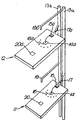
- first (11) and second (12) integrated circuits are coupled each to optical data highways 13a and 13b.
- Each circuit has an output pad 14, 14a whereby output signals from the circuit are coupled to a light emitting diode 15, 15a.
- This diode may be mounted on a common substrate or chip carrier adjacent the circuit or it may be integrated on the chip itself. In the latter case a diode material that is lattice matched to the chip should be employed. If for example a silicon chip is employed then a suitable diode material is zinc sulphide.
- Gallium arsenide chips may of course be provided with gallium arsenide based diodes.
- Each pad 14, 14a is coupled via a clock controlled electronic switch-16, 16a to a plurality of signal outputs whereby signals generated at those outputs may be time division multiplexed to form a common output signal.
- This common output signal is superimposed or modulated on to an optical signal via the . diode 15, 15a which optical signal is then coupled to the data highway 13, 13a via an input port 17, 17a.
- Each circuit 11, 12 has a plurality of photodetectors 20, 20a each associated with a circuit input and controlled via the circuit clock such that each output is enabled only during its respective time slot. For clarity only one photodetector is shown on each circuit. Incoming optical signals from the data highway 13 are received via an output port 19, 19a from which the light is broadcast over the circuit such that all the photodetectors are illuminated. Each photodetector thus responds only to that portion of the optical signal intended for that particular circuit input.
- the number of inputs and outputs may be equal.
- the number of inputs may be greater than, less than or equal to the number of outputs.
- each of the two circuits transmits to the other. It will however be apparent that the technique is not limited to this particular arrangement and that transmission to and from remote circuits (not shown) is also envisaged. Furthermore, although a guided transmission system is shown this may, in some applications, be replaced by free space transmission between adjacent circuits.
- the data pulses suffer substantially no degradation in shape during transmission between circuits. Furthermore there are no problems of impedance matching thus obviating the need for input and output buffer amplifiers.
- the high frequency of the light signal allows the simultaneous transmission of a large number of signals. For example, in a typical arrangement 50 outputs having bit rates of 5 Mbit/s may be multiplexed using a 250 M Hz connection rate.
- the major modification to the integrated circuit to implement the technique is the provision of commutated switching to selectively connect the output points of the circuit to the common output pad and to gate the photodetector inputs of the circuit in the required synchronism to effect the particular input connection pattern.
- This requires a clock generator on each chip running at the commutation rate. Typically this is provided by a master clock on one chip controlling slave generators on the other chips forming the system.
- the signal delay time between chips is less than the clock period and the system can thus be operated in absolute synchronism.
- each buffer being adaptively controlled to synchronize with the received data stream.
- the light source is solid state and may be a laser, LED or an electroluminescent element.
- Semiconductor diode sources have the capability for drive modulation rates up to 1 GHz and lasers have the capability for considerably higher modulation rates. In any particular configuration the source power required depends inter alia on the chip fan-out, losses in transmission, the modulation rate, the area of chip to be illuminated and the size of the photodetectors. The necessary calculation to take account of these factors will be apparent to those skilled in the art.
- a preferred mounting for the light source is adjacent the chip on a common chip support substrate.
- the commutated output pad may be connected to the source by a stitchbond, optionally via a buffer amplifier.
- the source is aligned with the input fibre to the optical bus harness, the input point being securely mounted adjacent the chip.
- the spectrum of the light is not critical but it should contain wavelengths, e.g. less than 1 micron, that are strongly absorbed in silicon.
- the input and output fibre ends to and from the bus have lens terminations.
- the photodetector may comprise an avalanche, photoconductive or PIN device and, advantageously, is monolithically integrated on the integrated circuit chip.
Landscapes
- Physics & Mathematics (AREA)
- Signal Processing (AREA)
- Optics & Photonics (AREA)
- Electromagnetism (AREA)
- Engineering & Computer Science (AREA)
- Computer Networks & Wireless Communication (AREA)
- General Physics & Mathematics (AREA)
- Optical Communication System (AREA)
- Electronic Switches (AREA)
- Design And Manufacture Of Integrated Circuits (AREA)
- Internal Circuitry In Semiconductor Integrated Circuit Devices (AREA)
- Photo Coupler, Interrupter, Optical-To-Optical Conversion Devices (AREA)
- Semiconductor Lasers (AREA)
Claims (5)
dadurch gekennzeichnet, daß Lichtwellenleitereinrichtungen vorgesehen sind, wodurch der modulierte optische Infrarot-Träger zwischen den Schaltungen übertragen wird.
dadurch gekennzeichnet, daß der Lichtwellenleiter eine Mehrmoden-Lichtleitfaser umfaßt.
dadurch gekennzeichnet, daß der Lichtwellenleiter Linsenausgangsabschlüsse aufweist, so daß die empfangenen optischen oder InfrarotSignale über jede Schaltung hinweg abgestrahlt werden.
Priority Applications (1)
| Application Number | Priority Date | Filing Date | Title |
|---|---|---|---|
| AT85302237T ATE54234T1 (de) | 1984-04-14 | 1985-04-01 | Zwischenverbindung von integrierten schaltungen. |
Applications Claiming Priority (2)
| Application Number | Priority Date | Filing Date | Title |
|---|---|---|---|
| GB8409751 | 1984-04-14 | ||
| GB08409751A GB2157488B (en) | 1984-04-14 | 1984-04-14 | Interconnecting integrated circuits |
Publications (3)
| Publication Number | Publication Date |
|---|---|
| EP0159832A2 EP0159832A2 (de) | 1985-10-30 |
| EP0159832A3 EP0159832A3 (en) | 1987-05-27 |
| EP0159832B1 true EP0159832B1 (de) | 1990-06-27 |
Family
ID=10559667
Family Applications (1)
| Application Number | Title | Priority Date | Filing Date |
|---|---|---|---|
| EP85302237A Expired - Lifetime EP0159832B1 (de) | 1984-04-14 | 1985-04-01 | Zwischenverbindung von integrierten Schaltungen |
Country Status (6)
| Country | Link |
|---|---|
| US (1) | US4682323A (de) |
| EP (1) | EP0159832B1 (de) |
| JP (1) | JPS60231361A (de) |
| AT (1) | ATE54234T1 (de) |
| DE (1) | DE3578490D1 (de) |
| GB (1) | GB2157488B (de) |
Families Citing this family (22)
| Publication number | Priority date | Publication date | Assignee | Title |
|---|---|---|---|---|
| GB2190789B (en) * | 1986-04-17 | 1990-05-09 | Plessey Co Plc | System for optically coupling components of integrated circuits |
| DE3640099A1 (de) * | 1986-11-24 | 1988-06-01 | Diehl Gmbh & Co | Baugruppenanordnung |
| US4882770A (en) * | 1987-12-14 | 1989-11-21 | H. M. Electronics, Inc. | Wireless optical communication system |
| US4959828A (en) * | 1988-05-31 | 1990-09-25 | Corporation Of The President Of The Church Of Jesus Christ Of Latter-Day Saints | Multi-channel infrared cableless communication system |
| US4850044A (en) * | 1988-06-23 | 1989-07-18 | International Business Machines Corporation | Serial optical interconnect bus for logic cards and the like |
| US5237441A (en) * | 1990-02-23 | 1993-08-17 | The United States Of America As Represented By The Secretary Of The Navy | Microprocessor chip incorporating optical signal coupling transceiver |
| DE4017997A1 (de) * | 1990-06-05 | 1991-12-12 | Siemens Ag | Optisches datenuebertragungssystem |
| US5087982A (en) * | 1990-11-14 | 1992-02-11 | Inter Innovation Lefebure Manufacturing | Pulsed communication system |
| US5250816A (en) * | 1991-04-08 | 1993-10-05 | Mitsubishi Denki Kabushiki Kaisha | Multichip system and method of supplying clock signal therefor |
| JPH05122159A (ja) * | 1991-05-13 | 1993-05-18 | Internatl Business Mach Corp <Ibm> | 伝送信号の信号対雑音比の改良方法及び光学的相互接続システム |
| EP0538552A3 (en) * | 1991-10-21 | 1993-10-06 | Rockwell International Corporation | High speed array processor bus |
| US5361272A (en) * | 1992-09-18 | 1994-11-01 | Stephen Krissman | Semiconductor architecture and application thereof |
| GB9306136D0 (en) * | 1993-03-24 | 1993-05-12 | Plessey Telecomm | Opto-electronic circuits |
| US5416861A (en) * | 1994-04-29 | 1995-05-16 | University Of Cincinnati | Optical synchronous clock distribution network and high-speed signal distribution network |
| US5761350A (en) * | 1997-01-22 | 1998-06-02 | Koh; Seungug | Method and apparatus for providing a seamless electrical/optical multi-layer micro-opto-electro-mechanical system assembly |
| US6453377B1 (en) * | 1998-06-16 | 2002-09-17 | Micron Technology, Inc. | Computer including optical interconnect, memory unit, and method of assembling a computer |
| US6221739B1 (en) | 1998-08-20 | 2001-04-24 | Vladimir A. Gorelik | Method for bonding single crystal membranes to a curved surface |
| US6771935B1 (en) * | 1998-10-05 | 2004-08-03 | Alcatel | Wireless bus |
| US6362907B1 (en) * | 1999-02-26 | 2002-03-26 | Nec Research Institute, Inc. | Apparatus and method for transmitting data between VLSI chips |
| US6788895B2 (en) | 1999-12-10 | 2004-09-07 | Altera Corporation | Security mapping and auto reconfiguration |
| US20030035173A1 (en) * | 2001-08-17 | 2003-02-20 | Byers Charles Calvin | Interconnecting processing units of a stored program controlled system using time division muliplexed free space optics |
| US8946905B2 (en) | 2011-06-27 | 2015-02-03 | Oracle International Corporation | Via structure for integrated circuits |
Family Cites Families (9)
| Publication number | Priority date | Publication date | Assignee | Title |
|---|---|---|---|---|
| GB961049A (en) * | 1961-06-07 | 1964-06-17 | Pye Ltd | Solid state circuits and micro circuits |
| DE2445419C3 (de) * | 1974-09-23 | 1979-12-20 | Siemens Ag, 1000 Berlin Und 8000 Muenchen | Schaltungsanordnung zum abwechselnden Auf schalten einer Anzahl von Signalsendern auf eine Anzahl von Signalempfängern |
| US4274104A (en) * | 1979-05-21 | 1981-06-16 | International Business Machines Corporation | Electrooptical integrated circuit communication |
| GB2069196B (en) * | 1980-02-05 | 1984-03-21 | Marconi Co Ltd | Processor arrangement |
| JPS5787635A (en) * | 1980-11-21 | 1982-06-01 | Showa Electric Wire & Cable Co Ltd | Optical wavelength multiplex signal transmitter |
| GB2101828B (en) * | 1981-07-14 | 1985-02-13 | Standard Telephones Cables Ltd | Exchange cabling |
| JPS5842333A (ja) * | 1981-09-07 | 1983-03-11 | Fujitsu Ltd | 装置内光伝送方式 |
| FR2517147A1 (fr) * | 1981-11-25 | 1983-05-27 | Telecommunications Sa | Systeme numerique de transmission d'informations par voie optique dit pluribus optique |
| US4533833A (en) * | 1982-08-19 | 1985-08-06 | At&T Bell Laboratories | Optically coupled integrated circuit array |
-
1984
- 1984-04-14 GB GB08409751A patent/GB2157488B/en not_active Expired
-
1985
- 1985-04-01 AT AT85302237T patent/ATE54234T1/de not_active IP Right Cessation
- 1985-04-01 EP EP85302237A patent/EP0159832B1/de not_active Expired - Lifetime
- 1985-04-01 DE DE8585302237T patent/DE3578490D1/de not_active Expired - Fee Related
- 1985-04-08 JP JP60074157A patent/JPS60231361A/ja active Pending
- 1985-04-12 US US06/723,491 patent/US4682323A/en not_active Expired - Lifetime
Also Published As
| Publication number | Publication date |
|---|---|
| EP0159832A2 (de) | 1985-10-30 |
| DE3578490D1 (de) | 1990-08-02 |
| ATE54234T1 (de) | 1990-07-15 |
| EP0159832A3 (en) | 1987-05-27 |
| US4682323A (en) | 1987-07-21 |
| GB2157488A (en) | 1985-10-23 |
| JPS60231361A (ja) | 1985-11-16 |
| GB2157488B (en) | 1987-09-16 |
Similar Documents
| Publication | Publication Date | Title |
|---|---|---|
| US4682323A (en) | Interconnecting integrated circuits | |
| US7356213B1 (en) | Transparent switch using optical and electrical proximity communication | |
| US7044658B1 (en) | High speed serial I/O technology using an optical link | |
| KR100794870B1 (ko) | 고속 메모리 시스템에서의 광 상호접속 | |
| US7840136B1 (en) | Low-latency switch using optical and electrical proximity communication | |
| EP0323000B1 (de) | Optische Rückwandverdrahtung | |
| JPH04170506A (ja) | 光コネクタ | |
| US5446572A (en) | Optical interconnects for high speed backplanes using spectral slicing | |
| GB2334396A (en) | Connecting circuit boards using optical WDM signals | |
| US5313536A (en) | Modular photonic waveguide distribution system | |
| AU1085701A (en) | Cluster integration approach to optical transceiver arrays and fiber bundles | |
| US6393184B1 (en) | Optical link between electrical circuit boards | |
| US6859571B2 (en) | Hybrid integration of electrical and optical chips | |
| US5202940A (en) | Modular electro-optic bus coupler system | |
| Hinton | Photonics in switching | |
| US7693424B1 (en) | Integrated proximity-to-optical transceiver chip | |
| CN208572096U (zh) | 双收双发设备及传输系统 | |
| US20050122154A1 (en) | Bi-directional signal level shift circuit | |
| US5777318A (en) | Smart pixel array using single diode for detection and modulation | |
| RU2028675C1 (ru) | Оптоэлектронный коммутатор | |
| JP2001237411A (ja) | 光電子集積回路装置 | |
| JPH09247092A (ja) | 光並列送信装置 | |
| US20260066993A1 (en) | Active optical interconnect with multiple light sources and method of modulation | |
| US5185833A (en) | Modular active fiber optic coupler system | |
| Kilcoyne et al. | Optical fiber crossbar switch |
Legal Events
| Date | Code | Title | Description |
|---|---|---|---|
| PUAI | Public reference made under article 153(3) epc to a published international application that has entered the european phase |
Free format text: ORIGINAL CODE: 0009012 |
|
| AK | Designated contracting states |
Designated state(s): AT BE CH DE FR IT LI LU NL SE |
|
| RAP1 | Party data changed (applicant data changed or rights of an application transferred) |
Owner name: STC PLC |
|
| RAP1 | Party data changed (applicant data changed or rights of an application transferred) |
Owner name: STC PLC |
|
| PUAL | Search report despatched |
Free format text: ORIGINAL CODE: 0009013 |
|
| AK | Designated contracting states |
Kind code of ref document: A3 Designated state(s): AT BE CH DE FR IT LI LU NL SE |
|
| 17P | Request for examination filed |
Effective date: 19870507 |
|
| 17Q | First examination report despatched |
Effective date: 19890615 |
|
| GRAA | (expected) grant |
Free format text: ORIGINAL CODE: 0009210 |
|
| AK | Designated contracting states |
Kind code of ref document: B1 Designated state(s): AT BE CH DE FR IT LI LU NL SE |
|
| PG25 | Lapsed in a contracting state [announced via postgrant information from national office to epo] |
Ref country code: SE Effective date: 19900627 Ref country code: LI Effective date: 19900627 Ref country code: IT Free format text: LAPSE BECAUSE OF FAILURE TO SUBMIT A TRANSLATION OF THE DESCRIPTION OR TO PAY THE FEE WITHIN THE PRESCRIBED TIME-LIMIT;WARNING: LAPSES OF ITALIAN PATENTS WITH EFFECTIVE DATE BEFORE 2007 MAY HAVE OCCURRED AT ANY TIME BEFORE 2007. THE CORRECT EFFECTIVE DATE MAY BE DIFFERENT FROM THE ONE RECORDED. Effective date: 19900627 Ref country code: CH Effective date: 19900627 Ref country code: BE Effective date: 19900627 Ref country code: AT Effective date: 19900627 |
|
| REF | Corresponds to: |
Ref document number: 54234 Country of ref document: AT Date of ref document: 19900715 Kind code of ref document: T |
|
| ET | Fr: translation filed | ||
| RAP2 | Party data changed (patent owner data changed or rights of a patent transferred) |
Owner name: STC PLC |
|
| REF | Corresponds to: |
Ref document number: 3578490 Country of ref document: DE Date of ref document: 19900802 |
|
| REG | Reference to a national code |
Ref country code: CH Ref legal event code: PL |
|
| PLBE | No opposition filed within time limit |
Free format text: ORIGINAL CODE: 0009261 |
|
| STAA | Information on the status of an ep patent application or granted ep patent |
Free format text: STATUS: NO OPPOSITION FILED WITHIN TIME LIMIT |
|
| PG25 | Lapsed in a contracting state [announced via postgrant information from national office to epo] |
Ref country code: LU Free format text: LAPSE BECAUSE OF NON-PAYMENT OF DUE FEES Effective date: 19910430 |
|
| 26N | No opposition filed | ||
| NLT1 | Nl: modifications of names registered in virtue of documents presented to the patent office pursuant to art. 16 a, paragraph 1 |
Owner name: STC LIMITED TE LONDEN, GROOT-BRITTANNIE. |
|
| NLT1 | Nl: modifications of names registered in virtue of documents presented to the patent office pursuant to art. 16 a, paragraph 1 |
Owner name: NORTHERN TELECOM EUROPE LIMITED TE LONDON, GROOT-B |
|
| REG | Reference to a national code |
Ref country code: FR Ref legal event code: TP |
|
| NLT1 | Nl: modifications of names registered in virtue of documents presented to the patent office pursuant to art. 16 a, paragraph 1 |
Owner name: STC LIMITED TE MAIDENHEAD, GROOT-BRITTANNIE. |
|
| NLS | Nl: assignments of ep-patents |
Owner name: NORTHERN TELECOM LIMITED IN MONTREAL, CANADA |
|
| PGFP | Annual fee paid to national office [announced via postgrant information from national office to epo] |
Ref country code: FR Payment date: 19990315 Year of fee payment: 15 |
|
| PGFP | Annual fee paid to national office [announced via postgrant information from national office to epo] |
Ref country code: NL Payment date: 19990325 Year of fee payment: 15 |
|
| PGFP | Annual fee paid to national office [announced via postgrant information from national office to epo] |
Ref country code: DE Payment date: 19990326 Year of fee payment: 15 |
|
| PG25 | Lapsed in a contracting state [announced via postgrant information from national office to epo] |
Ref country code: NL Free format text: LAPSE BECAUSE OF NON-PAYMENT OF DUE FEES Effective date: 20001101 |
|
| PG25 | Lapsed in a contracting state [announced via postgrant information from national office to epo] |
Ref country code: FR Free format text: LAPSE BECAUSE OF NON-PAYMENT OF DUE FEES Effective date: 20001229 |
|
| NLV4 | Nl: lapsed or anulled due to non-payment of the annual fee |
Effective date: 20001101 |
|
| PG25 | Lapsed in a contracting state [announced via postgrant information from national office to epo] |
Ref country code: DE Free format text: LAPSE BECAUSE OF NON-PAYMENT OF DUE FEES Effective date: 20010201 |
|
| REG | Reference to a national code |
Ref country code: FR Ref legal event code: ST |