EP0160183A2 - Transistor à effet de champ du type MOS pour haute tension - Google Patents
Transistor à effet de champ du type MOS pour haute tension Download PDFInfo
- Publication number
- EP0160183A2 EP0160183A2 EP85102631A EP85102631A EP0160183A2 EP 0160183 A2 EP0160183 A2 EP 0160183A2 EP 85102631 A EP85102631 A EP 85102631A EP 85102631 A EP85102631 A EP 85102631A EP 0160183 A2 EP0160183 A2 EP 0160183A2
- Authority
- EP
- European Patent Office
- Prior art keywords
- region
- semiconductor region
- semiconductor
- high voltage
- dielectric layer
- Prior art date
- Legal status (The legal status is an assumption and is not a legal conclusion. Google has not performed a legal analysis and makes no representation as to the accuracy of the status listed.)
- Withdrawn
Links
Images


Classifications
-
- H—ELECTRICITY
- H10—SEMICONDUCTOR DEVICES; ELECTRIC SOLID-STATE DEVICES NOT OTHERWISE PROVIDED FOR
- H10D—INORGANIC ELECTRIC SEMICONDUCTOR DEVICES
- H10D30/00—Field-effect transistors [FET]
- H10D30/60—Insulated-gate field-effect transistors [IGFET]
- H10D30/601—Insulated-gate field-effect transistors [IGFET] having lightly-doped drain or source extensions, e.g. LDD IGFETs or DDD IGFETs
- H10D30/603—Insulated-gate field-effect transistors [IGFET] having lightly-doped drain or source extensions, e.g. LDD IGFETs or DDD IGFETs having asymmetry in the channel direction, e.g. lateral high-voltage MISFETs having drain offset region or extended drain IGFETs [EDMOS]
-
- H—ELECTRICITY
- H10—SEMICONDUCTOR DEVICES; ELECTRIC SOLID-STATE DEVICES NOT OTHERWISE PROVIDED FOR
- H10D—INORGANIC ELECTRIC SEMICONDUCTOR DEVICES
- H10D62/00—Semiconductor bodies, or regions thereof, of devices having potential barriers
- H10D62/10—Shapes, relative sizes or dispositions of the regions of the semiconductor bodies; Shapes of the semiconductor bodies
- H10D62/13—Semiconductor regions connected to electrodes carrying current to be rectified, amplified or switched, e.g. source or drain regions
- H10D62/149—Source or drain regions of field-effect devices
- H10D62/151—Source or drain regions of field-effect devices of IGFETs
-
- H—ELECTRICITY
- H10—SEMICONDUCTOR DEVICES; ELECTRIC SOLID-STATE DEVICES NOT OTHERWISE PROVIDED FOR
- H10D—INORGANIC ELECTRIC SEMICONDUCTOR DEVICES
- H10D30/00—Field-effect transistors [FET]
- H10D30/60—Insulated-gate field-effect transistors [IGFET]
- H10D30/64—Double-diffused metal-oxide semiconductor [DMOS] FETs
- H10D30/66—Vertical DMOS [VDMOS] FETs
- H10D30/668—Vertical DMOS [VDMOS] FETs having trench gate electrodes, e.g. UMOS transistors
-
- H—ELECTRICITY
- H10—SEMICONDUCTOR DEVICES; ELECTRIC SOLID-STATE DEVICES NOT OTHERWISE PROVIDED FOR
- H10D—INORGANIC ELECTRIC SEMICONDUCTOR DEVICES
- H10D62/00—Semiconductor bodies, or regions thereof, of devices having potential barriers
- H10D62/10—Shapes, relative sizes or dispositions of the regions of the semiconductor bodies; Shapes of the semiconductor bodies
- H10D62/124—Shapes, relative sizes or dispositions of the regions of semiconductor bodies or of junctions between the regions
- H10D62/126—Top-view geometrical layouts of the regions or the junctions
-
- H—ELECTRICITY
- H10—SEMICONDUCTOR DEVICES; ELECTRIC SOLID-STATE DEVICES NOT OTHERWISE PROVIDED FOR
- H10D—INORGANIC ELECTRIC SEMICONDUCTOR DEVICES
- H10D64/00—Electrodes of devices having potential barriers
- H10D64/111—Field plates
-
- H—ELECTRICITY
- H10—SEMICONDUCTOR DEVICES; ELECTRIC SOLID-STATE DEVICES NOT OTHERWISE PROVIDED FOR
- H10D—INORGANIC ELECTRIC SEMICONDUCTOR DEVICES
- H10D84/00—Integrated devices formed in or on semiconductor substrates that comprise only semiconducting layers, e.g. on Si wafers or on GaAs-on-Si wafers
- H10D84/80—Integrated devices formed in or on semiconductor substrates that comprise only semiconducting layers, e.g. on Si wafers or on GaAs-on-Si wafers characterised by the integration of at least one component covered by groups H10D12/00 or H10D30/00, e.g. integration of IGFETs
- H10D84/82—Integrated devices formed in or on semiconductor substrates that comprise only semiconducting layers, e.g. on Si wafers or on GaAs-on-Si wafers characterised by the integration of at least one component covered by groups H10D12/00 or H10D30/00, e.g. integration of IGFETs of only field-effect components
- H10D84/83—Integrated devices formed in or on semiconductor substrates that comprise only semiconducting layers, e.g. on Si wafers or on GaAs-on-Si wafers characterised by the integration of at least one component covered by groups H10D12/00 or H10D30/00, e.g. integration of IGFETs of only field-effect components of only insulated-gate FETs [IGFET]
- H10D84/85—Complementary IGFETs, e.g. CMOS
- H10D84/856—Complementary IGFETs, e.g. CMOS the complementary IGFETs having different architectures than each other, e.g. high-voltage and low-voltage CMOS
Definitions
- the invention relates to semiconductor devices and methods of fabricating semiconductor devices, and more particularly to MOS field effect transistors capable of operating at high voltage.
- Meguro USP 4,285,116 discloses a high voltage MIS device using a lightly doped shallow diffusion region to connect the drain and source to the channel region.
- Ronen USP 4,288,802 ( Figure 10) discloses a high voltage MOSFET having a field plate 80 to bend lines away from the drain area, thereby increasing available breakdown adjacent the drain area.
- the device is laid out in concentric rings.
- the invention provides a high voltage MOS field effect transistor having a source and drain separated from each other by a deep n- well in the substrate of opposite conductivity, conductor with a distance between the drain and gate being relatively large.
- This n-well drift region is formed the same time as other n-wells where the p-channel devices reside in a n-well CMOS process.
- the metal which connects the source contact extends and overlaps the polygate region to form a field plate, reducing the electric field in the drift region.
- a preferred embodiment of the present invention has the structure implemented in a circular or elliptical format to avoid sharp corners.
- FIG. 1 there is shown the cross-section of the high voltage transistor with the low voltage CMOS logic devices.
- a 9-layer silicon gate LOCOS type n-wll CMOS process is used throughout our description for the fabrication of the device structures.
- the high voltage MOS device is n-channel and has an enclosed drain structure with metal field plate extending from the source node.
- the drain region is composed of a shallow n+ region made from the source/drain arsenic implant and a 6- ⁇ m deep phosphorus doped n-well drift region under the field oxide.
- This n-well drift region is formed by the same processing steps as other n-wells where the p-channel devices reside in the n-well CMOS process.
- the devices are fabricated on ⁇ 100>, 15-25 -cm p-type silicon.
- the high voltage MOSFET has the same threshold voltage as the low voltage n-channel device.
- the device is constructed on a p-type substrate 10 in which an n-well 11 is provided by means of diffusion or ion implantation according to techniques known in the art.
- An n+ drain region 12 is provided in the n-well 11, and an n+ source 13 is provided in the p type substrate 10 for forming the source. Both 12 and 13 regions are formed by ion implantation.
- a thick silicon dioxide region 14 is provided on the surface of the n-well 11 and extends into a much thinner oxide region 15 which is provided along the surface of the p type substrate between n-well 11 and the source region 13 and forms the gate oxide of the high voltage MOS device.
- Another thick field silicon dioxide region 16 is provided adjacent the n+ contact 13 to isolate the structure formed from other devices in the circuit to be constructed according to the present invention. The regions 14 and 16 are formed in the same oxidation cycle.
- a gate region 17 consisting of thin film polysilicon is deposited over the thin gate oxide 15 to form the polysilicon gate of the MOS field effect transistor formed according to the present invention.
- a low temperature oxide (LTO) layer 18 is then deposited over the silicon dioxide region 14 and the polysilicon gate 17 for electrically isolating such regions from the metal source contact.
- the metal source contact 19 is provided over the dielectric region 18 making contact with the n+ source 13 and extending over the gate polysilicon region 17 as well as a portion over the silicon dioxide region 14 and the n-well 11.
- FIG. 3 there is a shown a detailed top plan view of the embodiment of a portion of (between the x-x and y-y lines) the invention shown in Figure 1.
- the drain contact 12 and the source contact 13 regions there is shown the drain contact 12 and the source contact 13 regions.
- the n-well 11 extending adjacent to the n+ region 13 and separated therefrom by a distance labelled B in the figure.
- the distance between the n+ region 12 and the n+ region 13 is labelled L O in the figure.
- a polysilicon gate 17 is shown extending over portions of the n-well 11 as well as the n+ region 13.
- the polysilicon gate extends a distance A beyond the edge of the n+ region 13.
- the metal region 19 extends a distance L ST beyond the edge t of the n+ region 13.
- the width of the polysilicon gate 17 is C ano the width of the n+ region 13 is D.
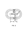
- FIG 2 there is shown a detailed top plan view of a first embodiment of an implementation of the present invention in which the invention has been laid out in circular or elliptical form.
- the drain 12 is shown to be in the middle surrounded by drift layer L D corresponding to the L D in Figure 3.
- the gate region 17 is then concentric with both the drain and the drift layer and has a width of L.
- the source is then concentric around the drain, drift layer and gate.
- Figure 4 is a cross-sectional view of the high voltage MUS field effect transistor integrated with both low voltage n channel and p channel transistors and are fabricated from the same process sequence.
- the left hand portion of the figure shows the high voltage n channel MOS transistor essentially as shown in Figure 1.
- the middle of the figure shows a low voltage n channel MOS transistor and the right hand portion of the figure shows a low voltage p channel MOS transistor.
- These n-channel and p-channel devices are used in the normal CMOS logic circuit.
- the high voltage MOS device can be used in the output driver stage.
- the semiconductor device according to the present invention can be implemented with various semiconductor technologies and different combinations of known process steps, and that the preferred embodiments illustrated here are merely exemplary.
- the depth of penetration of the various zones and regions and in particular the configuration and distance between the active zones of the transistor devices, as well as the concentrations of dopant species, and/or their concentration profiles, can be chosen depending upon the desired properties.
- the present invention is moreover not restricted to the particular embodiments of the high voltage MOSFET described.
- semiconductor materials other than silicon for example, A III -B v compounds may be used.
- the conductivity types in the embodiment may be Interchanged and corresponding to such change, the polarity of the respective operating voltages adapted.
- the voltage level and the static or dynamic nature of the signals applied to the various terminals and gates of the device, as well as the voltage sources, may be suitably selected as desired for a particular application.
- bipolar junction field effect transistor MNOS (metal electrode-silicon nitride, silicon oxide-semiconductor), MACS (metal, aluminum oxide, silicon oxide, semiconductor), MAS (metal, aluminum oxide, semiconductor), floating gate FETs, and AMOS FETs (avalanche MOS FETs), may be used as well.
- MNOS metal electrode-silicon nitride, silicon oxide-semiconductor
- MACS metal, aluminum oxide, silicon oxide, semiconductor
- MAS metal, aluminum oxide, semiconductor
- floating gate FETs floating gate FETs
- AMOS FETs avalanche MOS FETs
Landscapes
- Metal-Oxide And Bipolar Metal-Oxide Semiconductor Integrated Circuits (AREA)
- Electrodes Of Semiconductors (AREA)
- Insulated Gate Type Field-Effect Transistor (AREA)
Applications Claiming Priority (2)
| Application Number | Priority Date | Filing Date | Title |
|---|---|---|---|
| US60679784A | 1984-05-03 | 1984-05-03 | |
| US606797 | 1984-05-03 |
Publications (2)
| Publication Number | Publication Date |
|---|---|
| EP0160183A2 true EP0160183A2 (fr) | 1985-11-06 |
| EP0160183A3 EP0160183A3 (fr) | 1986-12-03 |
Family
ID=24429500
Family Applications (1)
| Application Number | Title | Priority Date | Filing Date |
|---|---|---|---|
| EP85102631A Withdrawn EP0160183A3 (fr) | 1984-05-03 | 1985-03-08 | Transistor à effet de champ du type MOS pour haute tension |
Country Status (2)
| Country | Link |
|---|---|
| EP (1) | EP0160183A3 (fr) |
| JP (1) | JPS60236268A (fr) |
Cited By (3)
| Publication number | Priority date | Publication date | Assignee | Title |
|---|---|---|---|---|
| US4801986A (en) * | 1987-04-03 | 1989-01-31 | General Electric Company | Vertical double diffused metal oxide semiconductor VDMOS device with increased safe operating area and method |
| US4823176A (en) * | 1987-04-03 | 1989-04-18 | General Electric Company | Vertical double diffused metal oxide semiconductor (VDMOS) device including high voltage junction exhibiting increased safe operating area |
| WO1990007794A1 (fr) * | 1988-12-23 | 1990-07-12 | Fraunhofer-Gesellschaft zur Förderung der angewandten Forschung e.V. | Transistor haute tension obtenu par technique cmos |
Families Citing this family (3)
| Publication number | Priority date | Publication date | Assignee | Title |
|---|---|---|---|---|
| JPS63164258A (ja) * | 1986-12-25 | 1988-07-07 | Fujitsu Ltd | 高耐圧入出力回路 |
| US5047358A (en) * | 1989-03-17 | 1991-09-10 | Delco Electronics Corporation | Process for forming high and low voltage CMOS transistors on a single integrated circuit chip |
| JP2530033B2 (ja) * | 1990-02-08 | 1996-09-04 | 株式会社東芝 | 絶縁ゲ―ト型集積回路 |
Family Cites Families (3)
| Publication number | Priority date | Publication date | Assignee | Title |
|---|---|---|---|---|
| US4058822A (en) * | 1975-05-30 | 1977-11-15 | Sharp Kabushiki Kaisha | High voltage, low on-resistance diffusion-self-alignment metal oxide semiconductor device and manufacture thereof |
| JPS5368581A (en) * | 1976-12-01 | 1978-06-19 | Hitachi Ltd | Semiconductor device |
| DE3046749C2 (de) * | 1979-12-10 | 1986-01-16 | Sharp K.K., Osaka | MOS-Transistor für hohe Betriebsspannungen |
-
1985
- 1985-03-08 EP EP85102631A patent/EP0160183A3/fr not_active Withdrawn
- 1985-04-16 JP JP60081211A patent/JPS60236268A/ja active Pending
Cited By (3)
| Publication number | Priority date | Publication date | Assignee | Title |
|---|---|---|---|---|
| US4801986A (en) * | 1987-04-03 | 1989-01-31 | General Electric Company | Vertical double diffused metal oxide semiconductor VDMOS device with increased safe operating area and method |
| US4823176A (en) * | 1987-04-03 | 1989-04-18 | General Electric Company | Vertical double diffused metal oxide semiconductor (VDMOS) device including high voltage junction exhibiting increased safe operating area |
| WO1990007794A1 (fr) * | 1988-12-23 | 1990-07-12 | Fraunhofer-Gesellschaft zur Förderung der angewandten Forschung e.V. | Transistor haute tension obtenu par technique cmos |
Also Published As
| Publication number | Publication date |
|---|---|
| JPS60236268A (ja) | 1985-11-25 |
| EP0160183A3 (fr) | 1986-12-03 |
Similar Documents
| Publication | Publication Date | Title |
|---|---|---|
| US6548874B1 (en) | Higher voltage transistors for sub micron CMOS processes | |
| US5427964A (en) | Insulated gate field effect transistor and method for fabricating | |
| US5438007A (en) | Method of fabricating field effect transistor having polycrystalline silicon gate junction | |
| US7375398B2 (en) | High voltage FET gate structure | |
| US5970338A (en) | Method of producing an EEPROM semiconductor structure | |
| US4891326A (en) | Semiconductor device and a process for manufacturing the same | |
| US6514824B1 (en) | Semiconductor device with a pair of transistors having dual work function gate electrodes | |
| EP0569204B1 (fr) | Procédé de fabrication des transistors à effet de champ à jonction à canal N et à canal P avec un procédé BiCMOS | |
| US5441906A (en) | Insulated gate field effect transistor having a partial channel and method for fabricating | |
| US7573098B2 (en) | Transistors fabricated using a reduced cost CMOS process | |
| JPH08107202A (ja) | 横型高耐圧電界効果トランジスタおよびその製造方法 | |
| US6376870B1 (en) | Low voltage transistors with increased breakdown voltage to substrate | |
| US20030127694A1 (en) | Higher voltage transistors for sub micron CMOS processes | |
| KR100962233B1 (ko) | 고전압 접합형 전계효과 트랜지스터 | |
| JPH08130308A (ja) | 半導体装置 | |
| US6030875A (en) | Method for making semiconductor device having nitrogen-rich active region-channel interface | |
| JP2003174160A (ja) | 横型高耐圧mosfet及びこれを備えた半導体装置 | |
| JPH0730107A (ja) | 高耐圧トランジスタ及びその製造方法 | |
| JPS6329967A (ja) | 半導体装置の製造方法 | |
| EP0160183A2 (fr) | Transistor à effet de champ du type MOS pour haute tension | |
| US6025238A (en) | Semiconductor device having an nitrogen-rich punchthrough region and fabrication thereof | |
| JPS61174667A (ja) | 半導体装置の製造方法 | |
| US20060284265A1 (en) | High voltage N-channel LDMOS devices built in a deep submicron CMOS process | |
| US8587055B2 (en) | Integrated circuit using a superjunction semiconductor device | |
| US6507058B1 (en) | Low threshold compact MOS device with channel region formed by outdiffusion of two regions and method of making same |
Legal Events
| Date | Code | Title | Description |
|---|---|---|---|
| PUAI | Public reference made under article 153(3) epc to a published international application that has entered the european phase |
Free format text: ORIGINAL CODE: 0009012 |
|
| AK | Designated contracting states |
Designated state(s): DE GB NL |
|
| PUAL | Search report despatched |
Free format text: ORIGINAL CODE: 0009013 |
|
| AK | Designated contracting states |
Kind code of ref document: A3 Designated state(s): DE GB NL |
|
| 17P | Request for examination filed |
Effective date: 19870519 |
|
| 17Q | First examination report despatched |
Effective date: 19881021 |
|
| STAA | Information on the status of an ep patent application or granted ep patent |
Free format text: STATUS: THE APPLICATION IS DEEMED TO BE WITHDRAWN |
|
| 18D | Application deemed to be withdrawn |
Effective date: 19890301 |
|
| RIN1 | Information on inventor provided before grant (corrected) |
Inventor name: CHOW, PEI-MING DANIEL |