EP0161896A2 - Schaltungsanordnung zur Halbwellengleichrichtung - Google Patents
Schaltungsanordnung zur Halbwellengleichrichtung Download PDFInfo
- Publication number
- EP0161896A2 EP0161896A2 EP85303212A EP85303212A EP0161896A2 EP 0161896 A2 EP0161896 A2 EP 0161896A2 EP 85303212 A EP85303212 A EP 85303212A EP 85303212 A EP85303212 A EP 85303212A EP 0161896 A2 EP0161896 A2 EP 0161896A2
- Authority
- EP
- European Patent Office
- Prior art keywords
- resistor
- coupled
- junction
- output terminal
- input signal
- Prior art date
- Legal status (The legal status is an assumption and is not a legal conclusion. Google has not performed a legal analysis and makes no representation as to the accuracy of the status listed.)
- Withdrawn
Links
Images


Classifications
-
- H—ELECTRICITY
- H03—ELECTRONIC CIRCUITRY
- H03D—DEMODULATION OR TRANSFERENCE OF MODULATION FROM ONE CARRIER TO ANOTHER
- H03D1/00—Demodulation of amplitude-modulated oscillations
- H03D1/22—Homodyne or synchrodyne circuits
- H03D1/2272—Homodyne or synchrodyne circuits using FET's
-
- G—PHYSICS
- G01—MEASURING; TESTING
- G01R—MEASURING ELECTRIC VARIABLES; MEASURING MAGNETIC VARIABLES
- G01R19/00—Arrangements for measuring currents or voltages or for indicating presence or sign thereof
- G01R19/22—Arrangements for measuring currents or voltages or for indicating presence or sign thereof using conversion of AC into DC
Definitions
- the present invention relates generally to electronic circuits, and more particularly to such circuits which generate, from an AC voltage input signal, a DC voltage output signal.
- Cost-effective half wave demodulators of the prior art utilised with a 400 Hz, 6 volt AC input signal, exhibit a ripple level in excess of 10 mv, and variations in output, from unit to unit, in excess of one per cent.
- the ripple level can be reduced by moving the filter poles to a lower frequency.
- servo-mechanisms that is not practical since additional, destabilising time lag in the signal results.
- This design possesses superior performance consistency from unit to unit but necessitates two reference signal generators 14 and 15, two switching transistors 16 and 17, and to effect demodulation, two operational amplifiers 18 and 19. Also, a pole of filtering entailing an additional operational amplifier 20a in a stage 20 is required after the demodulation stage, to achieve the desired pole configuration and ripple level.
- the present invention is defined in the appended claims and entails a half wave demodulation apparatus comprising means for generating an AC voltage input signal having a period comprising a first half period and a second half period. Means having an input terminal coupled to the generating means and having an output terminal, is utilised for switching off the AC voltage input signal during the first half period, and for switching on the AC voltage input signal during the second half period. A first means, having an input terminal coupled to the output terminal of the switching means and having an output terminal, is used for filtering the input signal. A second means for filtering the input signal has an input terminal coupled to the output terminal of the first filtering means.
- An operational amplifier has an inverting input terminal coupled to the input terminal of the second filtering means, and an output terminal coupled to an output terminal of the second filtering means.
- a first resistor has a first end coupled to a non-inverting input terminal of the operational amplifier and a second end coupled to ground.
- the switching means comprises a field-effect transistor having a source coupled to the input signal generating means.
- Means is utilised for generating a reference signal having a predetermined first voltage waveform during the first half period, and having a predetermined second voltage waveform during the second half period.
- a diode has an anode coupled to a gate of the field-effect transistor to form a first junction, and a cathode coupled to the reference signal generating means.
- a second resistor has a first end coupled to a junction of the input signal generating means and the source of the transistor, and a second end coupled to the first junction.
- Each of the filtering means in a preferred embodiment of the invention, comprises a resistor coupled to a capacitor.
- the present invention exhibits the performance consistency of the series full wave design of Figure 2, but entails less ripple.
- ripple current flows in the filters for the entire period of the AC voltage input dignal, whereas in the present invention the switching means is off for half a period and the first filter means during this interval sees only a steady discharge current through a resistor.
- the root mean square ripple level is reduced at the first filter means, and accordingly, throughout the entire circuit.
- the present invention when utilised with a 400 Hz, 6 volt AC input signal achieves approximately 3 mv ripple, and performance consistency, from unit to unit, of 0.1 per cent for filter poles at 20 rad/sec and 50 rad/sec.
- the present invention improves over the known series full wave circuit of Figure 2 by reducing the number of components and by incorporating both poles of filtering into a single operational amplifier system. This is accomplished with components which have multiple functions.
- the operational amplifier serves as an active one pole filter, buffers the output to supply a low source impedance, and acts as a current-to-voltage converter, whereby the first filter means sees a pure load resistance into a virtual ground.
- the present invention entails the following advantages over current designs: lowest ripple per filter pole; lowest component count for its unit-to-unit performance consistency; lowest count of critical resistors for its consistency; reduced operational amplifier count for its consistency; and lower cost for its consistency.
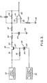
- the present invention entails an electronic circuit for converting an AC voltage input signal to a DC voltage output signal.
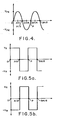
- An AC voltage input signal generator 30 provides an AC voltage input signal having period P, and peak voltage VPK , as illustrated in Figure 4.
- a reference square wave signal generator 31 provides a reference square wave signal, having a period P, whose axis crossings are synchronised with those of the AC voltage input signal.
- the reference square wave signal may be positive when the AC voltage input signal is positive, and negative when the AC voltage input signal is negative, or alternatively, as in Figure 5b, negative when the AC voltage input signal is positive, and positive when the AC voltage input signal is negative.
- the reference square wave signal alternates every half period between V R and, preferably, -V R . More generally, for an arbitrary, but fixed, period of the input signal, not necessarily coinciding with axis crossings, the reference square wave signal may be V R for half of the period and, preferably, -V R for the other half.
- the period of the AC input signal may be chosen to commence at P/4 and terminate at 5P/4.
- the reference signal may then be V R during the half period P/4 to 3P/4, and -V R for the half-period 3P/4 to 5P/4, or vice versa.
- a cathode 33 of a diode 34 is coupled to the reference square wave signal generator 31.
- An anode 35 of the diode 34 is coupled to a gate 37 of a field-effect transistor 38.
- a source 39 of the field-effect transistor 38 is coupled to the AC voltage input signal generator 30.
- a first end of a resistor 41 is coupled to the junction of the source 39 of the field-effect transistor 38 and the AC voltage input signal generator 30.
- the second end of the resistor 41 is coupled to the junction of the anode 35 of the diode 34 and the gate 37 of the field-effect transistor 38.
- a first end of a resistor 43 is coupled to a drain 44 of the field effect transistor 38.
- the second end of the resistor 43 is coupled to a first end of a resistor 45.
- the second end of the resistor 45 is coupled to a first end of a resistor 46.
- a first end of a capacitor 47 is coupled to ground 48, and the second end of the capacitor 47 is coupled to the junction of the resistor 43 and the resistor 45.
- a first end of a capacitor 49 is coupled to the junction of the resistor 45 and the resistor 46, and the second end of the capacitor 49 is coupled to the second end of the resistor 46.
- An inverting input terminal 50 of an operational amplifier 51 is coupled to the junction of the resistor 45 and the resistor 46.
- a non-inverting input terminal 52 of the operational amplifier 51 is coupled to a first end of a resistor 54, the second end of which is coupled to ground 55.
- An output terminal 56 of the operational amplifier 51 is coupled to the second end of the resistor 46.
- the AC voltage input signal generator 30 provides the AC voltage input signal illustrated in Figure 4.
- the reference square wave generator 31 provides a reference square wave signal which, relative to the AC voltage input signal, is preferably that of Figure 5a or that of Figure 5b. Wihtout loss of generality, the following description assumes a reference square wave signal which, relative to the AC voltage input signal, is as in Figure 5a.
- the voltage V R of the reference square wave signal is no less than the sum of the peak voltage Vp K of the AC voltage input signal, the forward bias voltage of the diode 34, and the gate-to-source cut-off voltage of the filed-effect transistor 38.
- the reference square wave signal of Figure 5a is positive, the diode 34 is reverse biased, and no current flows therethrough.
- the resistance of the resistor 43 is chosen to be approximately one-thousand times that of the field-effect transistor 38 when it is on.
- the resistor 43, the resistor 45 and the capacitor 47 form a filter which effects an averaging of the AC voltage input signal during this half-period.
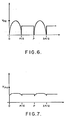
- the voltage that appears, during this half-period, at the junction of the resistor 43 and the capacitor 47 is 2/ ⁇ of the peak voltage V PK of the AC voltage input signal. This waveform is depicted in Figure 7 in the time interval 0 to P/2.
- the wave becomes, preferably, -V R volts, for a half-period.
- the diode 34 is conducting.
- the resistor 41 is selected with a resistance sufficient to isolate the AC voltage input signal from the reference square wave signal. Accordingly, a voltage of approximately -V R appears on the gate 37 of the field-effect transistor 38.
- the field-effect transistor 38 Since the difference between the voltage of the AC voltage input signal, which appears on the source 39, and the voltage -V R on the gate 37 is at least the gate-to-source cut-off voltage of the field-effect transistor 38, the field-effect transistor 38 is turned off during the half-period P/2 to P. No current flows through the resistor 43, and the voltage at the junction of the drain 44 of the field-effect transistor 38 and the resistor 43 is the voltage at the junction of the resistor 43 and the capacitor 47. This voltage, due to the filtering effect of the resistor 43, the resistor 45 and the capacitor 47, is essentially, as before 2/ ⁇ of the peak voltage VpK of the AC voltage input signal.
- Figure 6 depicts this voltage at the junction of the drain 44 and the resistor 43 by the waveform in the interval P/2 to P.
- Figure 7 depicts this voltage at the junction of the resistor 43 and the capacitor 47 by the waveform in the interval P/2 to P.
- this voltage declines exponentially but, in practice, it is essentially constant, owing to the small amount of time involved.
- the resistance of the resistor 45 is also chosen to be approximately one-thousand times that of the field-effect transistor 38 when it is on.
- the process begins again with the switching on of the field-effect transistor 38 by the positive square wave reference signal.
- the voltage appearing at the junction of the drain 44 and the resistor 43 during the interval P to 3P/2 is illustrated.
- This waveform is, of course, the same as that in the interval 0 to P/2.
- the voltage appearing at the junction of the resistor 43 and capacitor 47 during the interval P to 3P/2 is illustrated.
- This waveform is essentially a replica of the waveforms in the intervals 0 to P/2 and P/2 to P.
- the voltage appearing at the junction of the drain 44 and the resistor 43 consists of alternating, essentially identical, sinusoidal and square waveforms, each of duration P/2.
- the voltage appearing at the junction of the resistor 43 and the capacitor 47 consists of a substantially constant voltage, equal to 2/ ⁇ of Vp K' having a degree of ripple
- the resistor 54 is selected to have a resistance which is equal to that of the resistor 46 in parallel with a resistor having a resistance equal to twice that of the resistor 43 plus that of the resistor 45. That is, if the resistance of the resistor 43 is R 3 , if the resistance of the resistor 45 is R4, and if the resistance of the resistor 46 is R 5' then the resistance of the resistor 54 is chosen to be:- This choice is predicated upon the fact that this is the Thornton equivalent resistance seen from the inverting input terminal 50 of the operational amplifier 51. By providing the same resistance at the non-inverting input terminal 52 as at the inverting input terminal 50, both terminals experience the same voltage drop which ensures that there is no output of the operational amplifier 51 due to bias current of the operational amplifier when there is no input to the circuit.
- the voltage at the output terminal 56 of the operational amplifier 51 can be shown to be essentially a constant one, having a value:- If, relative to the AC voltage input signal, the reference square wave signal is as depicted in Figure 5b, then the voltage at the output terminal 56 is the negative of the above. More generally, the voltage at the output terminal 56 can be shown to be:--(2/ ⁇ ) (R 5 /(2R 3 + R 4 )V PK ⁇ cos( ⁇ ) where 9 is the angle of the input signal relative to the reference signal.
- the filter poles can be shown to be at:- where C l and C 2 are, respectively, the capacitances of the capacitors 47 and 49.
Landscapes
- Engineering & Computer Science (AREA)
- Power Engineering (AREA)
- Physics & Mathematics (AREA)
- General Physics & Mathematics (AREA)
- Networks Using Active Elements (AREA)
- Amplifiers (AREA)
- Rectifiers (AREA)
- Measurement Of Current Or Voltage (AREA)
Applications Claiming Priority (2)
| Application Number | Priority Date | Filing Date | Title |
|---|---|---|---|
| US60940284A | 1984-05-11 | 1984-05-11 | |
| US609402 | 1984-05-11 |
Publications (2)
| Publication Number | Publication Date |
|---|---|
| EP0161896A2 true EP0161896A2 (de) | 1985-11-21 |
| EP0161896A3 EP0161896A3 (de) | 1989-07-19 |
Family
ID=24440655
Family Applications (1)
| Application Number | Title | Priority Date | Filing Date |
|---|---|---|---|
| EP85303212A Withdrawn EP0161896A3 (de) | 1984-05-11 | 1985-05-07 | Schaltungsanordnung zur Halbwellengleichrichtung |
Country Status (3)
| Country | Link |
|---|---|
| EP (1) | EP0161896A3 (de) |
| JP (1) | JPS60245473A (de) |
| CA (1) | CA1228116A (de) |
Family Cites Families (2)
| Publication number | Priority date | Publication date | Assignee | Title |
|---|---|---|---|---|
| US3721891A (en) * | 1972-04-13 | 1973-03-20 | Lear Siegler Inc | Power normalized demodulator |
| EP0010900A1 (de) * | 1978-10-23 | 1980-05-14 | Era Patents Limited | Statischer Wechselrichter mit einer relativ niederfrequenten Ausgangsspannung und Verfahren zur Erzeugung dieser Spannung |
-
1985
- 1985-02-05 CA CA000473568A patent/CA1228116A/en not_active Expired
- 1985-03-12 JP JP4918685A patent/JPS60245473A/ja active Pending
- 1985-05-07 EP EP85303212A patent/EP0161896A3/de not_active Withdrawn
Also Published As
| Publication number | Publication date |
|---|---|
| CA1228116A (en) | 1987-10-13 |
| JPS60245473A (ja) | 1985-12-05 |
| EP0161896A3 (de) | 1989-07-19 |
Similar Documents
| Publication | Publication Date | Title |
|---|---|---|
| US4608541A (en) | Isolation amplifier | |
| JPH09511633A (ja) | パルスカウントfm復調器を具える受信機、及びパルスカウントfm復調器 | |
| HU212521B (en) | Circuit arrangement for supplying discharge lamps | |
| JPS6017170B2 (ja) | チヨツパ増幅器の復調回路 | |
| EP0161896A2 (de) | Schaltungsanordnung zur Halbwellengleichrichtung | |
| AU2016340016B2 (en) | A method and arrangement for controlling dimming to a lamp by a dimmer arrangement affected by ripple injection and/or superimposed supply authority ripple control signals upon the AC mains supply input wave signal | |
| EP0121278B1 (de) | Abschwächungsschaltung | |
| EP0256569A1 (de) | Versorgungsschaltung zur Speisung einer Lastimpedanz mit einem glatten Gleichstrom | |
| JPS6091426A (ja) | 電源装置 | |
| EP0080234A1 (de) | Filterschaltung mit einem Differentialverstärker | |
| AU566128B2 (en) | Sample and hold circuit | |
| US3225303A (en) | Modulating and demodulating apparatus | |
| RU2024169C1 (ru) | Устройство для управления тиристорным преобразователем | |
| KR0165889B1 (ko) | 전류차를 형성하기 위한 회로 | |
| FI67967B (fi) | Referensspaenningskaella | |
| KR920001698Y1 (ko) | 출력전압 귀환회로의 전압스파이크 클램핑회로 | |
| KR950025793A (ko) | 포커스 전압 가변 회로 및 이것을 내장한 플라이백 변압기 | |
| US5103389A (en) | Frequency range of analog converter by means of external rectifier | |
| JPH039391Y2 (de) | ||
| KR930012089B1 (ko) | 수직 편향회로 | |
| SU1012223A1 (ru) | Стабилизированный преобразователь посто нного напр жени | |
| SU1518871A1 (ru) | Двухполупериодный выпр митель | |
| JPH0453050Y2 (de) | ||
| JPS58166817A (ja) | 可変利得増幅装置 | |
| KR910007623Y1 (ko) | 스테레오 오디오 신호의 레벨차를 감소하기 위한 회로 |
Legal Events
| Date | Code | Title | Description |
|---|---|---|---|
| PUAI | Public reference made under article 153(3) epc to a published international application that has entered the european phase |
Free format text: ORIGINAL CODE: 0009012 |
|
| AK | Designated contracting states |
Designated state(s): DE FR GB IT NL |
|
| RAP1 | Party data changed (applicant data changed or rights of an application transferred) |
Owner name: HONEYWELL INC. |
|
| PUAL | Search report despatched |
Free format text: ORIGINAL CODE: 0009013 |
|
| AK | Designated contracting states |
Kind code of ref document: A3 Designated state(s): DE FR GB IT NL |
|
| 17P | Request for examination filed |
Effective date: 19900105 |
|
| 17Q | First examination report despatched |
Effective date: 19901206 |
|
| STAA | Information on the status of an ep patent application or granted ep patent |
Free format text: STATUS: THE APPLICATION IS DEEMED TO BE WITHDRAWN |
|
| 18D | Application deemed to be withdrawn |
Effective date: 19910618 |
|
| RIN1 | Information on inventor provided before grant (corrected) |
Inventor name: DICKEY, JOHN ALVIN |