EP0164747A2 - Analog-Digitalwandler mit schrittweiser Annäherung mit veränderlicher Taktfrequenz - Google Patents
Analog-Digitalwandler mit schrittweiser Annäherung mit veränderlicher Taktfrequenz Download PDFInfo
- Publication number
- EP0164747A2 EP0164747A2 EP85107269A EP85107269A EP0164747A2 EP 0164747 A2 EP0164747 A2 EP 0164747A2 EP 85107269 A EP85107269 A EP 85107269A EP 85107269 A EP85107269 A EP 85107269A EP 0164747 A2 EP0164747 A2 EP 0164747A2
- Authority
- EP
- European Patent Office
- Prior art keywords
- signal
- digital
- analog
- clock
- pulses
- Prior art date
- Legal status (The legal status is an assumption and is not a legal conclusion. Google has not performed a legal analysis and makes no representation as to the accuracy of the status listed.)
- Withdrawn
Links
Images
Classifications
-
- H—ELECTRICITY
- H03—ELECTRONIC CIRCUITRY
- H03M—CODING; DECODING; CODE CONVERSION IN GENERAL
- H03M1/00—Analogue/digital conversion; Digital/analogue conversion
- H03M1/12—Analogue/digital converters
- H03M1/34—Analogue value compared with reference values
- H03M1/38—Analogue value compared with reference values sequentially only, e.g. successive approximation type
- H03M1/40—Analogue value compared with reference values sequentially only, e.g. successive approximation type recirculation type
-
- H—ELECTRICITY
- H03—ELECTRONIC CIRCUITRY
- H03M—CODING; DECODING; CODE CONVERSION IN GENERAL
- H03M1/00—Analogue/digital conversion; Digital/analogue conversion
- H03M1/12—Analogue/digital converters
- H03M1/34—Analogue value compared with reference values
- H03M1/38—Analogue value compared with reference values sequentially only, e.g. successive approximation type
- H03M1/46—Analogue value compared with reference values sequentially only, e.g. successive approximation type with digital/analogue converter for supplying reference values to converter
Definitions
- the present invention relates to a means for converting analog signals to digital signals and more particularly for optimizing the speed of such of conversions in a way that avoids high-cost logic components.
- Analog-to-digital converters are frequently used in applications which call for a delay of an analog electrical signal. For example, in television systems it is frequently necessary to delay the audio portion of a composite audio-visual signal to compensate for various delays in the video portion of the signal which are occasioned by signal processing and/or signal enhancement requirements. Usually the types of processing/enhancement circuits required for video are not required for audio, and absent some means for delaying the audio signal, there would be no means for correlating the audio with the video portion of the composite signal.
- a common technique used in the past has been to convert the audio, which is essentially an analog signal, to a digital signal and delay the signal with a digital delay line. Digital delay lines are particularly desirable for this purpose as they are inherently more accurate than analog-type delay lines.
- the successive approximation A/D converters utilize a special-purpose shift register which contains the digital logic necessary to effect the A/D conversion. These operate on a sampled and held portion of an analog signal. For each portion of the analog signal sampled, the successive approximation A/D converter completes a series of approximation cycles driven by clock pulses in which each cycle determines a bit of binary resolution for the digital value representing the analog signal. Depending upon the number of bits of resolution required, there will be "n" number of clock cycles to derive a digital value from the sampled analog signal.
- Successive approximation A/D converters are closed loop systems, however, having inherent propagation and settling delays. The largest of these delays is caused by a digital-to-analog converter (DAC) which converts a digital approximation of the sampled analog signal to a second analog signal for successive comparisons with the sampled analog signal.
- DAC digital-to-analog converter
- the heart of this type of A/D converter is a successive approximation register (SAR) which begins each series of cycles at a specified initial value for the digital word and toggles that word one bit during each clock cycle beginning with most significant digit.
- the resulting digital approximation is converted to an analog signal in the DAC and compared to the sampled analog signal.
- the SAR updates the digital word for that particular bit of resolution. Since the SAR begins with the most significant digit, the widest swings in the output of the DAC occur during this first clock cycle.
- the DAC usually includes an output voltage amplifier which has a slew rate that is slow compared to the remaining components in the circuit.
- the slew rate of the output amplifier is, thus, the primary limiting factor in the speed of this type of A/D converter.
- the slew rate is less of a limitation on bits of lesser significance in the digital word, because the analog voltage representative of these bits is progressively less than that required for the most significant bit in the digital word.
- the clock which controls each of the N number of cycles during each sampling period must provide the time required for the output voltage amplifier to rise to the maximum output needed for the most significant bit. This time may also be thought of as the loop settling time.
- the present invention addresses the problem of the inherent limitations of a successive approximation analog-to-digital converter by varying the clock frequency as a function of the time required for the loop voltage to rise to the level required, i.e. to a steady state value. This time is a function of the slew rate of the voltage output amplifier multiplied by the amplitude of the voltage swing required to approximate the "nth" significant digit of the digital word.
- the present invention solves the above-mentioned problem and provides a faster analog-to-digital conversion by periodically adjusting the frequency of the clock during the sampling period.
- the analog-to-digital converter of the present invention comprises an SAR loop driven by a variable frequency clock.
- the loop consists of an analog comparator having an input from a sample and hold circuit for sampling the analog signal.
- the other input to the comparator is the output of a digital-to-analog converter which consists of a current DAC and an output voltage amplifier.
- Analog-to-digital conversion is controlled by an SAR.
- the SAR supplies the current DAC with an initial predetermined digital word which is assumed to lie at approximately the midpoint of the analog values expected to be encountered.
- the current D AC converts the digital word to an analog current which, in turn, is converted to an analog voltage by the voltage amplifier. This voltage is compared to the sampled and held analog voltage and an output is produced.
- the output of the comparator is either "high” or “low” depending upon whether the sampled voltage is higher or lower than loop voltage.
- the comparator output then toggles the SAR by one digit, updating the digital word to approximate the value of the analog voltage for each "nth" bit of binary resolution.
- This digital value is, in turn, converted to an analog voltage and the process is repeated for the next decreasingly significant bit of binary information.
- the conversion process is complete to the "nth" significant digit. This process is repeated for each analog data sample.
- the SAR responds to a clock which generates "n" cycles of clock pulses per sampling period.
- the frequency of the clock pulses may be, according to the invention, adjusted to compensate for differences in the loop settling time which is in part a function of the voltage amplifier's slew rate times the voltage swing required for the "nth" significant digit.
- the overall loop settling time is also a function of the transient behavior of the loop after the voltage rises to the level required. After a rapid voltage rise, the loop may oscillate or ring before settling out to a steady state value. For example, since the successive approximation register proceeds from the most significant to the least significant digit, the largest voltage swings will occur on the first approximation.
- the clock must enable the SAR for as long as required for the loop voltage to rise to and settle upon its steady state value. Since the next successive approximation, however, will be a less significant digit, the voltage swing will not be as large and, therefore, the loop settling time will be smaller.
- the frequency of the clock may be adjusted so that the SAR is enabled for a shorter period of time when voltage swings of lesser magnitude are expected.
- the loop settling times become progressively shorter as the SAR proceeds from most significant to least significant digit.
- each output cycle of the clock needs to have a pulse width only sufficiently long to ensure that the loop voltage has settled to its steady-state value as demanded by the "nth" significant digit of the digital word. In other words, as the output swing of the DAC and voltage amplifier decreases, the clock frequency increases. In this way the speed of the loop is maximized for each sampling period.
- a principal object of this invention is to provide analog-to-digital conversion for an electrical signal which is fast and accurate.
- a further object of this invention is to provide fast analog-to-digital conversion using relatively inexpensive components.
- a still further object of this invention is to provide analog-to-digital conversion using a successive approximation loop driven by a variable frequency clock to make most efficient use of the successive approximation technique.
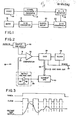
- FIG. 1 a television system utilizing the A/D converter of the present invention is shown.
- the system comprises a video channel 10 and an audio channel 12.
- the video channel signal is subject to various signal processing and/or signal enhancement circuits shown schematically at 14.
- a necessary result of the use of circuits 14 is an inherent delay of the video signal before it can be displayed on audio-visual monitor 16.
- a delay line is provided for in the audio channel 12.
- This delay line comprises an A/D converter 18 connected to a digital delay device 20, the output of which is reconverted to an analog audio signal in digital-to-analog converter 22.
- FIG. 2 shows the preferred form of the analog-to-digital converter 18 for use in the system of FI G. 1.
- This A/D converter is a successive approximation type, and as such includes a successive approximation shift register 24.
- Successive approximation register (SAR) 24 is connected to clock 26.
- the initiation of the operation of both SAR 24 and clock 26 is controlled by synchronization line 28 which is connected to an appropriate sync generator (not shown).
- the audio output of audio generator 12 is connected to input of sample-and-hold-circuit 30 and the output of the sample-and-hold circuit is connected to one of two inputs of comparator 32.
- the other input to comparator 32 is the output of output voltage amp 34.
- output voltage amp 34 comprises operational amplifier 36 and a shunt resistor 38.
- the output voltage amplifier 36 has an input which is connected to the output of a current digital-to-analog converter (DAC) 40.
- DAC digital-to-analog converter
- the output line 42 of the successive approximation register is the digital data output which is connected to digital delay device 20 and also drives current DAC 40 in order to complete a closed loop system.
- the output of audio amplifier 12 is periodically sampled and held at a predetermined sampling rate by sample-and-hold circuit 30. Initiation of a sampling period turns on clock 26 which begins to cycle through a program of clock pulses having predetermined pulse widths. The number of. clock pulses during each cycle depends upon the number of bits of binary resolution required for each analog-to-digital conversion during a sampling period. The result is that at the end of a sampling period, digital delay device 20 has accumulated a digital word expressed in binary form having "n" bits of binary resolution. This digital word is representative of the analog value sampled by sample-and-hold circuit 30 during a particular sampling period.
- the SAR begins each sampling period with its digital output word at a specified initial value.
- This initial value is converted to an analog voltage by current DAC 40 and output voltage amplifier 34 and appears as an input to comparator 32 on line 33.
- the sampled and held voltage from the audio generator 12 appears also as an input to comparator 32 on line 31.
- the output of comparator 32 is either "high” or “low” depending upon whether the voltage on line 33 is higher or lower than the voltage on line 31.
- the high/low output of comparator 32 causes the successive approximation register to update the preprogrammed digital word one bit at a time depending upon the comparator output. For example, if the comparator output is high and the present value of the digital word for that bit is a "zero", the zero is replaced with a one.
- the loop Since the loop is a closed loop system, and further since this system involves a conversion of a digital word to an analog voltage, there is a finite response time for the loop voltage to settle to a steady-state value for each-successive approximation.
- the primary limiting factor in the speed of the loop is the slew rate of the output voltage amplifier 34.
- the settling time for the loop can never be faster than the slew rate times the voltage swing required by the value of the output of the current DAC 40. This voltage swing will be larger for the more significant bits in the binary word.
- the loop completes one bit of approximation per clock pulse and should settle to a steady-state value before the next clock pulse begins. Therefore, the width of the pulses from clock 26 must be at least long enough to accommodate the loop settling time for the largest output voltage swings required of output voltage amplifier 34.
- the clock is therefore programmed to decrease the width of the clock pulses as the SAR progresses from most to least significant bit.
- the frequency of the clock should vary inversely with the overall loop settling time which comprises the slew rate times the voltage swing of amplifier 34 plus the loop transient settling time.
- FIG. 3 a pulse on synchronization line 28 initiates a programmed series of clock pulses from clock 26.
- the clock pulses fall into two groups, the first two pulses having double the frequency of the last four pulses.
- the amplifier output must rise to its maximum value on the first pulse.
- the voltage swing is half as large in terms of absolute value.
- the voltage swings required are much smaller because less significant bits of the digital word are being approximated.
- the "guesses" which form the output of output voltage amp 34 move closer and closer to the true analog value on line 31.
- the graph of FIG. 3 is intended to show the probable shape of a curve for the output voltage amplifier 34 over a sampling period in which the sampled analog value is approximately half of its expected full-scale value.
- clock output may be adjusted to any combination of decreasing pulse widths from most significant to least significant binary bit. However, there will always be at least two pulses in each cycle in which one pulse width will be longer than the next succeeding pulse width to accommodate for the differences in loop settling time and thus allow the loop to operate faster on bits of lesser significance.
- Implementation of the clock may be by several methods.
- the clock may take the form of a voltage-controlled oscillator controlled by a voltage ramp.
- the clock could be implemented by an N state divider having successive states separated by fewer and fewer states.
- Still a third method would be to use a Programmable Read Only Memory (PROM) controlled by a counter, where the clock pulses are the output of the PROM.
- PROM Programmable Read Only Memory
Landscapes
- Engineering & Computer Science (AREA)
- Theoretical Computer Science (AREA)
- Analogue/Digital Conversion (AREA)
Applications Claiming Priority (2)
| Application Number | Priority Date | Filing Date | Title |
|---|---|---|---|
| US62023284A | 1984-06-13 | 1984-06-13 | |
| US620232 | 1984-06-13 |
Publications (1)
| Publication Number | Publication Date |
|---|---|
| EP0164747A2 true EP0164747A2 (de) | 1985-12-18 |
Family
ID=24485110
Family Applications (1)
| Application Number | Title | Priority Date | Filing Date |
|---|---|---|---|
| EP85107269A Withdrawn EP0164747A2 (de) | 1984-06-13 | 1985-06-12 | Analog-Digitalwandler mit schrittweiser Annäherung mit veränderlicher Taktfrequenz |
Country Status (2)
| Country | Link |
|---|---|
| EP (1) | EP0164747A2 (de) |
| JP (1) | JPS6112123A (de) |
Cited By (3)
| Publication number | Priority date | Publication date | Assignee | Title |
|---|---|---|---|---|
| US4983969A (en) * | 1987-12-23 | 1991-01-08 | Kabushiki Kaisha Toshiba | Successive approximation analog to digital converter |
| EP1916770A1 (de) * | 2006-10-26 | 2008-04-30 | Atmel Nantes Sa | Analog-Digital-Wandler mit schrittweiser Annäherung, integrierte Schaltung, die einen solchen Analog-Digital-Wandler umfasst, und entsprechendes Verfahren |
| CN109905128A (zh) * | 2019-03-15 | 2019-06-18 | 上海胤祺集成电路有限公司 | 一种自适应的高速sar-adc转换时间完全利用电路及方法 |
Families Citing this family (1)
| Publication number | Priority date | Publication date | Assignee | Title |
|---|---|---|---|---|
| JPH02159814A (ja) * | 1988-12-14 | 1990-06-20 | Hitachi Ltd | チョッパ型コンパレータ |
Family Cites Families (3)
| Publication number | Priority date | Publication date | Assignee | Title |
|---|---|---|---|---|
| JPS50159661A (de) * | 1974-06-12 | 1975-12-24 | ||
| JPS5115363A (ja) * | 1974-07-29 | 1976-02-06 | Hitachi Ltd | Anaroguudejitaruhenkanki |
| JPS5591233A (en) * | 1978-12-28 | 1980-07-10 | Fujitsu Ltd | Successive comparison type a/d converter |
-
1985
- 1985-06-12 EP EP85107269A patent/EP0164747A2/de not_active Withdrawn
- 1985-06-13 JP JP60129082A patent/JPS6112123A/ja active Pending
Cited By (5)
| Publication number | Priority date | Publication date | Assignee | Title |
|---|---|---|---|---|
| US4983969A (en) * | 1987-12-23 | 1991-01-08 | Kabushiki Kaisha Toshiba | Successive approximation analog to digital converter |
| EP1916770A1 (de) * | 2006-10-26 | 2008-04-30 | Atmel Nantes Sa | Analog-Digital-Wandler mit schrittweiser Annäherung, integrierte Schaltung, die einen solchen Analog-Digital-Wandler umfasst, und entsprechendes Verfahren |
| FR2907986A1 (fr) * | 2006-10-26 | 2008-05-02 | Atmel Nantes Sa Sa | Convertisseur analogique/numerique a approximations successives,composant integre et procede de conversion correspondants. |
| US7576678B2 (en) | 2006-10-26 | 2009-08-18 | Atmel Nantes Sa | Successive approximation analog/digital converter and associated integrated component and conversion method |
| CN109905128A (zh) * | 2019-03-15 | 2019-06-18 | 上海胤祺集成电路有限公司 | 一种自适应的高速sar-adc转换时间完全利用电路及方法 |
Also Published As
| Publication number | Publication date |
|---|---|
| JPS6112123A (ja) | 1986-01-20 |
Similar Documents
| Publication | Publication Date | Title |
|---|---|---|
| US4345241A (en) | Analog-to-digital conversion method and apparatus | |
| CA1124868A (en) | Charge redistribution circuits | |
| EP0559657B1 (de) | Zweistufiger a/d-wandler unter verwendung von doppel-multiplexwandlern mit gemeinsamer schrittweiser annährungssteuerung | |
| CN103078643B (zh) | 连续逼近缓存器模拟至数字转换器以及相关控制方法 | |
| EP0401245B1 (de) | Digital-analogwandler | |
| US5028926A (en) | Successive type analog-to-digital converter with a variable reference voltage for the digital to analog converter | |
| US4968989A (en) | Switched capacitor filter for use with a digital-to-analog (D/A) converter | |
| US7102559B2 (en) | Analog-to-digital converter having interleaved coarse sections coupled to a single fine section | |
| US20040174286A1 (en) | Digital to analog convertor | |
| US6340943B1 (en) | Analog to digital converter method and apparatus | |
| US5283583A (en) | High-speed A/D conversion using a series of one-bit conversion stages | |
| US5691722A (en) | Direct-digitizing, self stabilizing analog to digital converter | |
| US3781871A (en) | Analog to digital converter | |
| US4369433A (en) | Digital-to-analog converter and PCM encoder using the converter | |
| US5105194A (en) | Time shift two-step analog to digital converter | |
| CN110808737A (zh) | 用于异步sar-adc的延迟链电路的数字校正方法 | |
| JPS6112123A (ja) | 逐次比較型アナログ・デジタル変換器 | |
| US4905006A (en) | Digital-to-analog converter | |
| JPH0645936A (ja) | アナログ・デジタル変換方式 | |
| EP0836768A1 (de) | Monolitischer analog-digital-wandler | |
| US3868678A (en) | Analogue-to-digital convertors | |
| JP4540829B2 (ja) | アナログデジタルコンバータ | |
| KR100189748B1 (ko) | 고속 연속 근사 a/d 변환기 | |
| JPH05211442A (ja) | アナログ・ディジタル変換器の試験方法 | |
| KR102140007B1 (ko) | 연속 근사 레지스터 아날로그 디지털 변환기 및 이를 이용한 아날로그 디지털 변환 방법 |
Legal Events
| Date | Code | Title | Description |
|---|---|---|---|
| PUAI | Public reference made under article 153(3) epc to a published international application that has entered the european phase |
Free format text: ORIGINAL CODE: 0009012 |
|
| AK | Designated contracting states |
Designated state(s): DE FR GB NL |
|
| STAA | Information on the status of an ep patent application or granted ep patent |
Free format text: STATUS: THE APPLICATION IS DEEMED TO BE WITHDRAWN |
|
| 18D | Application deemed to be withdrawn |
Effective date: 19870701 |
|
| RIN1 | Information on inventor provided before grant (corrected) |
Inventor name: DAVIDSON, SCOTT A. |