EP0401245B1 - Digital-analogwandler - Google Patents
Digital-analogwandler Download PDFInfo
- Publication number
- EP0401245B1 EP0401245B1 EP89902275A EP89902275A EP0401245B1 EP 0401245 B1 EP0401245 B1 EP 0401245B1 EP 89902275 A EP89902275 A EP 89902275A EP 89902275 A EP89902275 A EP 89902275A EP 0401245 B1 EP0401245 B1 EP 0401245B1
- Authority
- EP
- European Patent Office
- Prior art keywords
- sources
- digital
- selection
- input
- source
- Prior art date
- Legal status (The legal status is an assumption and is not a legal conclusion. Google has not performed a legal analysis and makes no representation as to the accuracy of the status listed.)
- Expired - Lifetime
Links
- 238000001228 spectrum Methods 0.000 claims abstract description 13
- 238000006243 chemical reaction Methods 0.000 claims description 14
- 238000005070 sampling Methods 0.000 claims description 10
- 230000000694 effects Effects 0.000 claims description 7
- 238000000034 method Methods 0.000 claims description 6
- 230000004044 response Effects 0.000 claims description 4
- 230000008859 change Effects 0.000 claims description 2
- 238000007493 shaping process Methods 0.000 claims description 2
- 125000004122 cyclic group Chemical group 0.000 abstract 1
- 229920005994 diacetyl cellulose Polymers 0.000 description 4
- 238000010586 diagram Methods 0.000 description 3
- 238000013459 approach Methods 0.000 description 2
- 238000007796 conventional method Methods 0.000 description 1
- 230000001419 dependent effect Effects 0.000 description 1
- 230000007246 mechanism Effects 0.000 description 1
- 230000008569 process Effects 0.000 description 1
Images


Classifications
-
- H—ELECTRICITY
- H03—ELECTRONIC CIRCUITRY
- H03M—CODING; DECODING; CODE CONVERSION IN GENERAL
- H03M1/00—Analogue/digital conversion; Digital/analogue conversion
- H03M1/06—Continuously compensating for, or preventing, undesired influence of physical parameters
- H03M1/0617—Continuously compensating for, or preventing, undesired influence of physical parameters characterised by the use of methods or means not specific to a particular type of detrimental influence
- H03M1/0634—Continuously compensating for, or preventing, undesired influence of physical parameters characterised by the use of methods or means not specific to a particular type of detrimental influence by averaging out the errors, e.g. using sliding scale
- H03M1/0656—Continuously compensating for, or preventing, undesired influence of physical parameters characterised by the use of methods or means not specific to a particular type of detrimental influence by averaging out the errors, e.g. using sliding scale in the time domain, e.g. using intended jitter as a dither signal
- H03M1/066—Continuously compensating for, or preventing, undesired influence of physical parameters characterised by the use of methods or means not specific to a particular type of detrimental influence by averaging out the errors, e.g. using sliding scale in the time domain, e.g. using intended jitter as a dither signal by continuously permuting the elements used, i.e. dynamic element matching
- H03M1/0665—Continuously compensating for, or preventing, undesired influence of physical parameters characterised by the use of methods or means not specific to a particular type of detrimental influence by averaging out the errors, e.g. using sliding scale in the time domain, e.g. using intended jitter as a dither signal by continuously permuting the elements used, i.e. dynamic element matching using data dependent selection of the elements, e.g. data weighted averaging
-
- H—ELECTRICITY
- H03—ELECTRONIC CIRCUITRY
- H03M—CODING; DECODING; CODE CONVERSION IN GENERAL
- H03M1/00—Analogue/digital conversion; Digital/analogue conversion
- H03M1/66—Digital/analogue converters
- H03M1/74—Simultaneous conversion
- H03M1/742—Simultaneous conversion using current sources as quantisation value generators
- H03M1/747—Simultaneous conversion using current sources as quantisation value generators with equal currents which are switched by unary decoded digital signals
Definitions
- This invention relates to a digital to analogue converter (DAC) and in particular to an n bit DAC of the kind having at least 2 n -1 sources, where the sources may be current, charge or voltage sources, most typically current sources.
- DAC digital to analogue converter
- the DAC of the invention is intended more especially but not exclusively for use in oversampling analogue to digital converters (ADC's).
- a DAC is a device that will output an analogue parameter, usually a voltage, current, or charge, that is representation of a digital input to it.
- an 8 bit digital word can have one of 256 values, so an 8 bit DAC will output a voltage or current which can have one of 256 different values. Since the analogue values which can be output are limited in number, any particular analogue value produced is accurate only within upper and lower limits. Thus, digitally, each one of the 256 different values is precisely defined, whereas the analogue output can only have a defined degree of accuracy associated with it. There is no absolute agreement on the precise definition of accuracy but an 8 bit, 8 bit accuracy DAC will output analogue voltage or currents which are +/- 0.5 lsbs accurate.
- Multibit high accuracy oversampling ACDs require DACs which have relatively few bits (say 4 to 8) and are very accurate (say +/- 0.01 lsbs). Another way of describing the accuracy required is that a DAC of n bits with m bit accuracy is needed, where m >> n. Such DACs are very difficult to construct and 16 bits for m is the currently available limit, although in theory 18 bits or more would be required.
- DACs may incorporate current sources, where the current sources have different values.
- One conventional technique is, for an 8 bit DAC, to use 8 current sources which are each a factor of 2 larger than the next one.
- One digital input control line is then connected to each current source.
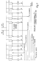
- Another technique, feasible with the advent of VLSI, for the same 8 bit DAC, is to use 255 equal current sources, where the msb digital control line switches on 128 sources, the next switches 64, the next 32, and so on, as diagrammatically indicated in Figure 1.
- an n bit DAC needs at least 2 n -1 current sources.
- An example of a DAC acting in this way is disclosed in EP 0253950, wherein the sources are switched a multiplicity of times during each sample.
- Oversampling ADCs put a low accuracy ADC with an accurate DAC in a feedback loop, and sample the signal many (eg 128) times faster than the required rate.
- the effect of the feedback loop is to correlate up quantising noise from the ADC in such a way that the noise spectrum is shaped, and is very low in the required part of the spectrum.
- a digital filter on the output of the ADC then filters out all signals (including noise from the unwanted parts of the spectrum, and then decimates the output data rate, frequency shifting it if necessary.
- the wanted part of the spectrum is usually, but not always, the low frequency part (eg the first 1/28th) of the spectrum.
- an n bit DAC comprises means for sampling a digital signal in response to a signal from a sampling clock; at least 2 n -1 digital input lines to which the samples of the digital signal are fed in succession; at least 2 n -1 current charge or voltage sources; at least 2 n -1 source switches, each associated with a respective source and operable to switch that source in response to an input from a digital input line; a 2 n -1 to 2 n -1 digital switching circuit; characterised in that the digital switching circuit is operable to change the selection of switches cyclically only once per cycle of the sampling signal, the selection of sources remaining unchanged during the conversion of each sample, and wherein, in use, a first digital input turns on s1 current sources to effect digital to analogue conversion, a second digital input turns on s2 further current sources to effect digital to analogue conversion and said source control means continues, for each digital input, to select sources in this way until at any selection step the number of selected sources exceeds the total number of sources whereupon source selection
- the changes of selection between different samples is such as to convert errors in the magnitudes of the sources into signals appearing in the unwanted parts of the spectrum of the converted signal.
- a method of converting an n-bit digital signal into an analogue signal comprises the steps of:
- the closest prior art approach to this technique is to select the sources randomly.
- the present invention shows substantial advantages over both selection in an absolutely fixed manner and random selection.
- one conversion may require the digital word "3" to be converted, and current sources 2, 5, 8 are chosen, whilst on the next conversion, to convert "3" sources, 11, 16, 4 are chosen, etc.
- the selection algorithm is desirably chosen first of all to convert DAC errors into noise, and secondly and most importantly to put all (or most) of that noise energy in the unwanted parts of the spectrum.
- the mechanism by which it does this is different from the way a basic oversampling ADC works and is entirely dependent on the algorithm.
- an n-bit DAC in accordance with the invention as 2 n current sources (one more than is absolutely necessary) and operates in accordance with an algorithm, on the basis of which the current sources are selected in the following manner.
- a digital input requiring s1 current sources to be turned on selects the first s1.
- the next conversion requires s2 current sources, and selects s2, starting from s1+1. If this requires sources beyond 2 n , counting starts again from the beginning, and the final sources used is designated q(L).
- the next conversion requires s3 sources, and selects s3 using q(L+1) as the first.
- the process continues and infinitum.
- the block diagram of Figure 2A illustrates the basic system.
- reference 10 denotes the n digital inputs.
- a decoder operating in accordance with the algorithm is referenced 12, and is associated with an n-loop (or n th order) feedback circuit 14 for shaping the quantising noise.
- Reference 16 denotes the switchable current sources and reference 18 designates the output.
- a sample clock input to the decoder is referenced 20.
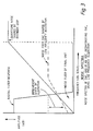
- Figure 3 shows the noise spectrum of the DAC in accordance with the invention, and is labelled in self-explanatory manner.
- the algorithm producing the noise spectrum of Figure 3 can reduce the accuracy requirements for the current sources by at least a factor of 30 in an oversampling ADC using a 3 bit DAC, and oversampling by at least 16 times. It makes feasible multibit oversamplers with a resolution substantially in excess of 18 bits.
Landscapes
- Engineering & Computer Science (AREA)
- Theoretical Computer Science (AREA)
- Analogue/Digital Conversion (AREA)
- Oscillators With Electromechanical Resonators (AREA)
- Networks Using Active Elements (AREA)
- Compression, Expansion, Code Conversion, And Decoders (AREA)
- Control Of Eletrric Generators (AREA)
Claims (5)
- Ein n-bit-Digital/Analogwandler mit Mitteln zum Abtasten eines Digitalsignals nach Maßgabe eines Signales von einem Abtast-Zeittaktgeber, mit mindestens 2n-1 digitalen Eingangsleitungen, denen die Abtastungen des Digitalsignals nacheinander zugeführt werden, mit mindestens 2n-1 Strom-, Ladungs- oder Spannungsquellen, mit mindestens 2n-1 Quellenschaltern, von denen jeder mit einer entsprechenden Quelle zusammenwirkt und betätigbar ist, um die Quelle nach Maßgabe eines Eingangssignals von einer digitalen Eingangsleitung zu schalten, und mit einem 2n-1 bis 2n-1 digitalen Schaltkreis, dadurch gekennzeichnet, daß der digitale Schaltkreis betätigbar ist, um die Auswahl der Schalter zyklisch nur einmal pro Zyklus des Abtastsignals zu ändern, die Auswahl der Quellen während der Wandlung jeder Abtastung unverändert bleibt, und wobei bei Gebrauch eine erste digitale Eingabe s1 Stromquellen zum Bewirken einer Digital/Analogwandlung einschaltet, eine zweite digitale Eingabe s2 weitere Stromquellen zum Bewirken einer Digital/Analogwandlung einschaltet und das besagte Quellensteuermittel die Auswahl der Quellen auf diese Weise für jede digitale Eingabe fortsetzt, bis bei irgendeiner Auswahlstufe die letzte der ausgewählten Quellen die Gesamtzahl der Quellen überschreiten würde, worauf die Quellenauswahl bei einer der besagten s1 Quellen erneut beginnt.
- Ein n-bit-Digital/Analogwandler nach Anspruch 1 mit 2n Stromquellen, wobei der digitale Schaltkreis Steuermittel enthält, wodurch eine erste digitale Eingabe s1 Stromquellen zum Bewirken einer Digital/Analogwandlung einschaltet, eine zweite digitale Eingabe s2 Stromquellen zum Bewirken einer Digital/Analogwandlung einschaltet, die Auswahl der besagten s2 Quellen von der Quelle s1+1 beginnt und das besagte Quellensteuermittel die Auswahl der Quellen auf diese Weise bei jeder digitalen Eingabe fortsetzt, bis bei irgendeiner Auswahlstufe die Zahl der ausgewählten Quellen 2n übersteigt, worauf die Quellenauswahl bei der ersten Quelle erneut beginnt.
- Ein n-bit-Digital/Analogwandler nach Anspruch 1 oder Anspruch 2, wobei die Quellenauswahlschaltung einen mindestens 2n-1 bis 2n-1 Multiplexer umfaßt, der durch einen bei Gebrauch an den Abtast-Zeittaktgeber angeschlossenen, im Zeittakt geschalteten Eingang stufenweise geschaltet wird.
- Ein n-bit-Digital/Analogwandler nach Anspruch 1 oder Anspruch 2, wobei die Quellenauswahlschaltung einen Decoder umfaßt, der in Übereinstimmung mit dem Algorithmus und nach Maßgabe eines bei Gebrauch an den Abtast-Zeittaktgeber angeschlossenen, im Zeittakt geschalteten Eingangs arbeitet, wobei der Digital/Analogwandler zum Formen des quantisierenden Geräuschs einen Teil einer n-Schleifen-Rückkopplungsschaltung bildet.
- Ein Verfahren zum Umwandeln eines n-bit-Digitalsignales in ein Analogsignal, enthaltend die folgenden Stufen:(a) Abtasten des Digitalsignals zum Bilden einer Aufeinanderfolge von Abtastungen, von denen jede einen Wert im Bereich von 0 bis 2n-1 darstellt, und Umwandeln jeder Eingabe in einen Thermometercode,(b) Zuführen des Codes für jede Abtastung nacheinander auf 2n-1 Eingangsleitungen und für jede Eingangsleitung, der ein Signal zugeführt wird, Schalten einer ausgewählten von 2n-1 Strom-, Spannungs- oder Ladungsquellen, wobei die Gesamtzahl der geschalteten Quellen dem Wert der Eingangsabtastung entspricht,(c) Zusammenfügen der Ausgaben der geschalteten Quellen,(d) bei einer anschließenden Abtastung von weniger als 2n-1 Ändern der Auswahl der Quellen zyklisch in Relation zu den Eingabeleitungen und(e) Wiederholen der obigen Stufen (a) bis (d) für sich an schließende digitale Eingaben, dadurch gekennzeich- net, daß die Auswahl der Quellen während der Umwandlung jeder Abtastung unverändert bleibt und daß die Änderungen der Auswahl zwischen verschiedenen Abtastungen dergestalt sind, daß Fehler in den Größen der Quellen in in den unerwünschten Teilen des Spektrums des umgewandelten Signales erscheinende Signale umgewandelt werden.
Applications Claiming Priority (3)
| Application Number | Priority Date | Filing Date | Title |
|---|---|---|---|
| GB888803627A GB8803627D0 (en) | 1988-02-17 | 1988-02-17 | Digital to analogue converter |
| GB8803627 | 1988-02-17 | ||
| PCT/GB1989/000112 WO1989007862A1 (en) | 1988-02-17 | 1989-02-10 | Digital to analogue converter |
Publications (2)
| Publication Number | Publication Date |
|---|---|
| EP0401245A1 EP0401245A1 (de) | 1990-12-12 |
| EP0401245B1 true EP0401245B1 (de) | 1995-06-07 |
Family
ID=10631846
Family Applications (1)
| Application Number | Title | Priority Date | Filing Date |
|---|---|---|---|
| EP89902275A Expired - Lifetime EP0401245B1 (de) | 1988-02-17 | 1989-02-10 | Digital-analogwandler |
Country Status (7)
| Country | Link |
|---|---|
| US (1) | US5138317A (de) |
| EP (1) | EP0401245B1 (de) |
| JP (1) | JPH03502864A (de) |
| AT (1) | ATE123605T1 (de) |
| DE (1) | DE68922989T2 (de) |
| GB (1) | GB8803627D0 (de) |
| WO (1) | WO1989007862A1 (de) |
Families Citing this family (26)
| Publication number | Priority date | Publication date | Assignee | Title |
|---|---|---|---|---|
| EP0597123A4 (de) * | 1992-06-01 | 1998-05-13 | Digital-analogwandler und analog-digitalwandler. | |
| US5313300A (en) * | 1992-08-10 | 1994-05-17 | Commodore Electronics Limited | Binary to unary decoder for a video digital to analog converter |
| US5243347A (en) * | 1992-09-28 | 1993-09-07 | Motorola, Inc. | Monotonic current/resistor digital-to-analog converter and method of operation |
| US5760726A (en) * | 1996-08-23 | 1998-06-02 | Motorola, Inc. | Digital-to-analog converter with dynamic matching and bit splitting |
| JP2002504277A (ja) * | 1997-04-18 | 2002-02-05 | イェスパー ステーンスガール−メイセン | 非線形分離および線形再接合に基づくオーバサンプルされたディジタル・アナログ変換器 |
| US6124813A (en) * | 1997-06-06 | 2000-09-26 | Analog Devices, Inc. | Self-linearizing multi-bit DACs |
| US6348884B1 (en) | 1999-01-06 | 2002-02-19 | Jesper Steensgaard-Madsen | Idle-tone-free mismatch-shaping encoders |
| US6816100B1 (en) | 1999-03-12 | 2004-11-09 | The Regents Of The University Of California | Analog-to-digital converters with common-mode rejection dynamic element matching, including as used in delta-sigma modulators |
| DE19912447C2 (de) * | 1999-03-19 | 2002-02-28 | Micronas Gmbh | Anordnung zum Erzeugen eines in seiner Bitbreite begrenzten digitalen Signals und Digital/Analog-Umsetzer mit vergrößertem Wertebereich |
| EP1100203B1 (de) * | 1999-11-10 | 2005-12-28 | Fujitsu Limited | Rauschformung in segmentierten Schaltungen für gemischte Signalen |
| SE522440C2 (sv) * | 2000-01-31 | 2004-02-10 | Ericsson Telefon Ab L M | Omvandlare |
| JP3725001B2 (ja) | 2000-03-28 | 2005-12-07 | 株式会社東芝 | 選択回路、d/a変換器及びa/d変換器 |
| DE60015958T2 (de) * | 2000-08-10 | 2005-12-01 | Stmicroelectronics S.R.L., Agrate Brianza | Digital-analog-wandlerschaltung |
| US6531973B2 (en) * | 2000-09-11 | 2003-03-11 | Broadcom Corporation | Sigma-delta digital-to-analog converter |
| US6577261B2 (en) | 2000-09-11 | 2003-06-10 | Broadcom Corporation | Method and apparatus for mismatched shaping of an oversampled converter |
| DE60119476T2 (de) * | 2000-10-26 | 2006-11-23 | Fujitsu Ltd., Kawasaki | Segmentierte Schaltungsanordnung |
| US6522277B2 (en) | 2001-02-05 | 2003-02-18 | Asahi Kasei Microsystems, Inc. | Circuit, system and method for performing dynamic element matching using bi-directional rotation within a data converter |
| EP1461867A2 (de) * | 2001-12-18 | 2004-09-29 | Koninklijke Philips Electronics N.V. | Digital-analog-wandler |
| DE102005012444B4 (de) * | 2005-03-17 | 2006-12-07 | Infineon Technologies Ag | Steuervorrichtung und Verfahren zur Verwürfelung der Zuordnung der Referenzen eines Quantisierers in einem Sigma-Delta-Analog-Digital-Umsetzer |
| US7420494B1 (en) | 2007-04-30 | 2008-09-02 | Analog Devices, Inc. | Mismatch shaping Δ-Σ analog to digital converter system |
| US7692569B2 (en) * | 2008-04-03 | 2010-04-06 | Analog Devices, Inc. | Methods and apparatus for rotating a thermometer code |
| GB2463663A (en) * | 2008-09-19 | 2010-03-24 | Data Conversion Systems Ltd | Computer audio interface unit which generates a word clock and computer synchronization based on an independent reference signal |
| WO2013175476A1 (en) | 2012-05-25 | 2013-11-28 | Audio Pixels Ltd. | A system, a method and a computer program product for controlling a group of actuator arrays for producing a physical effect |
| DK2856770T3 (en) | 2012-05-25 | 2018-10-22 | Audio Pixels Ltd | SYSTEM, PROCEDURE AND COMPUTER PROGRAM PRODUCT TO CONTROL A SET OF ACTUATOR ELEMENTS |
| US12451895B2 (en) | 2022-10-28 | 2025-10-21 | Kepler Computing Inc. | Mismatch shaping apparatus and method for binary coded digital-to-analog converters |
| US12438549B2 (en) | 2023-01-27 | 2025-10-07 | Analog Devices, Inc. | Apparatuses and methods for efficient shuffling in a digital to analog converter |
Family Cites Families (12)
| Publication number | Priority date | Publication date | Assignee | Title |
|---|---|---|---|---|
| NL7405441A (nl) * | 1974-04-23 | 1975-10-27 | Philips Nv | Nauwkeurige stroombronschakeling. |
| NL8003948A (nl) * | 1980-07-09 | 1982-02-01 | Philips Nv | Digitaal-analoog omzetter. |
| JPS61240716A (ja) * | 1985-04-17 | 1986-10-27 | Mitsubishi Electric Corp | ディジタルアナログコンバ−タ |
| JPH0697743B2 (ja) * | 1985-04-17 | 1994-11-30 | 株式会社日立製作所 | オ−バサンプル形d/a変換器 |
| JPS62183627A (ja) * | 1986-02-07 | 1987-08-12 | Sony Corp | デジタルデ−タの処理方式 |
| JPS62287717A (ja) * | 1986-06-06 | 1987-12-14 | Matsushita Electric Ind Co Ltd | デイジタル・アナログ変換回路 |
| JPS62292023A (ja) * | 1986-06-11 | 1987-12-18 | Nec Corp | D−a変換器 |
| JPS62296626A (ja) * | 1986-06-16 | 1987-12-23 | Nec Corp | D−aコンバ−タ |
| EP0253950B1 (de) * | 1986-07-21 | 1991-07-17 | Deutsche ITT Industries GmbH | Monolithisch integrierter Digital/Analog-Wandler |
| DE3778554D1 (de) * | 1987-12-10 | 1992-05-27 | Itt Ind Gmbh Deutsche | Digital/analog-wandler mit zyklischer ansteuerung von stromquellen. |
| NL8703128A (nl) * | 1987-12-24 | 1989-07-17 | Philips Nv | Digitaal-analoog-omzetter. |
| US4864215A (en) * | 1988-02-16 | 1989-09-05 | U.S. Philips Corp. | Current source arrangement |
-
1988
- 1988-02-17 GB GB888803627A patent/GB8803627D0/en active Pending
-
1989
- 1989-02-10 AT AT89902275T patent/ATE123605T1/de not_active IP Right Cessation
- 1989-02-10 EP EP89902275A patent/EP0401245B1/de not_active Expired - Lifetime
- 1989-02-10 JP JP1502111A patent/JPH03502864A/ja active Pending
- 1989-02-10 US US07/555,162 patent/US5138317A/en not_active Expired - Lifetime
- 1989-02-10 DE DE68922989T patent/DE68922989T2/de not_active Expired - Lifetime
- 1989-02-10 WO PCT/GB1989/000112 patent/WO1989007862A1/en not_active Ceased
Also Published As
| Publication number | Publication date |
|---|---|
| GB8803627D0 (en) | 1988-03-16 |
| WO1989007862A1 (en) | 1989-08-24 |
| EP0401245A1 (de) | 1990-12-12 |
| US5138317A (en) | 1992-08-11 |
| DE68922989D1 (de) | 1995-07-13 |
| ATE123605T1 (de) | 1995-06-15 |
| DE68922989T2 (de) | 1995-11-02 |
| JPH03502864A (ja) | 1991-06-27 |
Similar Documents
| Publication | Publication Date | Title |
|---|---|---|
| US5138317A (en) | Digital to analogue converter adapted to select input sources based on a preselected algorithm once per cycle of a sampling signal | |
| EP0559657B1 (de) | Zweistufiger a/d-wandler unter verwendung von doppel-multiplexwandlern mit gemeinsamer schrittweiser annährungssteuerung | |
| EP0793876B1 (de) | Analoger digitalwandler mit variabler abtastrate | |
| US4890106A (en) | Apparatus and methods for digital-to-analog conversion using modified LSB switching | |
| CA2004317C (en) | Successive comparison type analog-to-digital converting apparatus | |
| US6239734B1 (en) | Apparatus and a method for analog to digital conversion using plural reference signals and comparators | |
| US6147632A (en) | Sampling frequency conversion apparatus and fractional frequency dividing apparatus for sampling frequency conversion | |
| WO1996016482A9 (en) | Variable sample rate adc | |
| US5463395A (en) | Semi-flash type A/D converter employing a correction encoder for eliminating errors in the output signals due to noise, and a corresponding method therefor | |
| JPH10336487A (ja) | アナログ/ディジタル変換回路 | |
| EP1588492B1 (de) | Analog/digital-umsetzungsanordnung, verfahren zur analog/digital-umsetzung und signalverarbeitungssystem, worin die umsetzungsanordnung angewandt wird | |
| US4937579A (en) | Method of converting analog signals into digital signals and system for carrying out the method | |
| GB2089606A (en) | Analog-to-digital converter circuits | |
| US5726653A (en) | Tri-step analog-to-digital converter | |
| US5084701A (en) | Digital-to-analog converter using cyclical current source switching | |
| JP2001345700A (ja) | A/d変換回路 | |
| WO1998008298A1 (en) | Voltage-to-frequency converter | |
| JPH05276036A (ja) | A/dコンバータのオフセット補償回路 | |
| JP2001292064A (ja) | Ad変換回路 | |
| US11722143B2 (en) | ADC apparatus and control method | |
| USRE34660E (en) | Apparatus and methods for digital-to-analog conversion using modified LSB switching | |
| JPH07231256A (ja) | アナログ/ディジタル変換器 | |
| JPH04346521A (ja) | A/d変換回路 | |
| KR100339542B1 (ko) | 고속 아날로그/디지털 변환기 | |
| JPH04235418A (ja) | Ad変換器 |
Legal Events
| Date | Code | Title | Description |
|---|---|---|---|
| PUAI | Public reference made under article 153(3) epc to a published international application that has entered the european phase |
Free format text: ORIGINAL CODE: 0009012 |
|
| 17P | Request for examination filed |
Effective date: 19900724 |
|
| AK | Designated contracting states |
Kind code of ref document: A1 Designated state(s): AT BE CH DE FR GB IT LI LU NL SE |
|
| 17Q | First examination report despatched |
Effective date: 19920831 |
|
| ITF | It: translation for a ep patent filed | ||
| GRAA | (expected) grant |
Free format text: ORIGINAL CODE: 0009210 |
|
| AK | Designated contracting states |
Kind code of ref document: B1 Designated state(s): AT BE CH DE FR GB IT LI LU NL SE |
|
| PG25 | Lapsed in a contracting state [announced via postgrant information from national office to epo] |
Ref country code: AT Effective date: 19950607 Ref country code: BE Effective date: 19950607 Ref country code: LI Effective date: 19950607 Ref country code: CH Effective date: 19950607 |
|
| REF | Corresponds to: |
Ref document number: 123605 Country of ref document: AT Date of ref document: 19950615 Kind code of ref document: T |
|
| ET | Fr: translation filed | ||
| REF | Corresponds to: |
Ref document number: 68922989 Country of ref document: DE Date of ref document: 19950713 |
|
| PG25 | Lapsed in a contracting state [announced via postgrant information from national office to epo] |
Ref country code: SE Effective date: 19950907 |
|
| REG | Reference to a national code |
Ref country code: CH Ref legal event code: PL |
|
| PG25 | Lapsed in a contracting state [announced via postgrant information from national office to epo] |
Ref country code: LU Free format text: LAPSE BECAUSE OF NON-PAYMENT OF DUE FEES Effective date: 19960229 |
|
| PLBE | No opposition filed within time limit |
Free format text: ORIGINAL CODE: 0009261 |
|
| STAA | Information on the status of an ep patent application or granted ep patent |
Free format text: STATUS: NO OPPOSITION FILED WITHIN TIME LIMIT |
|
| 26N | No opposition filed | ||
| REG | Reference to a national code |
Ref country code: GB Ref legal event code: IF02 |
|
| PGFP | Annual fee paid to national office [announced via postgrant information from national office to epo] |
Ref country code: DE Payment date: 20080320 Year of fee payment: 20 Ref country code: NL Payment date: 20080325 Year of fee payment: 20 Ref country code: GB Payment date: 20080213 Year of fee payment: 20 |
|
| PGFP | Annual fee paid to national office [announced via postgrant information from national office to epo] |
Ref country code: FR Payment date: 20080313 Year of fee payment: 20 |
|
| PGFP | Annual fee paid to national office [announced via postgrant information from national office to epo] |
Ref country code: IT Payment date: 20080329 Year of fee payment: 20 |
|
| REG | Reference to a national code |
Ref country code: GB Ref legal event code: PE20 Expiry date: 20090209 |
|
| NLV7 | Nl: ceased due to reaching the maximum lifetime of a patent |
Effective date: 20090210 |
|
| PG25 | Lapsed in a contracting state [announced via postgrant information from national office to epo] |
Ref country code: NL Free format text: LAPSE BECAUSE OF EXPIRATION OF PROTECTION Effective date: 20090210 |
|
| PG25 | Lapsed in a contracting state [announced via postgrant information from national office to epo] |
Ref country code: GB Free format text: LAPSE BECAUSE OF EXPIRATION OF PROTECTION Effective date: 20090209 |