EP0164924A2 - Procédé pour améliorer le recouvrement d'une marche par des diélectriques dans les circuits intégrés à très grande échelle - Google Patents
Procédé pour améliorer le recouvrement d'une marche par des diélectriques dans les circuits intégrés à très grande échelle Download PDFInfo
- Publication number
- EP0164924A2 EP0164924A2 EP85303445A EP85303445A EP0164924A2 EP 0164924 A2 EP0164924 A2 EP 0164924A2 EP 85303445 A EP85303445 A EP 85303445A EP 85303445 A EP85303445 A EP 85303445A EP 0164924 A2 EP0164924 A2 EP 0164924A2
- Authority
- EP
- European Patent Office
- Prior art keywords
- thickness
- dielectric layer
- deposited
- dielectric
- further characterized
- Prior art date
- Legal status (The legal status is an assumption and is not a legal conclusion. Google has not performed a legal analysis and makes no representation as to the accuracy of the status listed.)
- Withdrawn
Links
Images

Classifications
-
- H—ELECTRICITY
- H10—SEMICONDUCTOR DEVICES; ELECTRIC SOLID-STATE DEVICES NOT OTHERWISE PROVIDED FOR
- H10P—GENERIC PROCESSES OR APPARATUS FOR THE MANUFACTURE OR TREATMENT OF DEVICES COVERED BY CLASS H10
- H10P95/00—Generic processes or apparatus for manufacture or treatments not covered by the other groups of this subclass
- H10P95/06—Planarisation of inorganic insulating materials
- H10P95/062—Planarisation of inorganic insulating materials involving a dielectric removal step
- H10P95/064—Planarisation of inorganic insulating materials involving a dielectric removal step the removal being chemical etching
-
- H—ELECTRICITY
- H10—SEMICONDUCTOR DEVICES; ELECTRIC SOLID-STATE DEVICES NOT OTHERWISE PROVIDED FOR
- H10P—GENERIC PROCESSES OR APPARATUS FOR THE MANUFACTURE OR TREATMENT OF DEVICES COVERED BY CLASS H10
- H10P50/00—Etching of wafers, substrates or parts of devices
- H10P50/20—Dry etching; Plasma etching; Reactive-ion etching
- H10P50/28—Dry etching; Plasma etching; Reactive-ion etching of insulating materials
- H10P50/282—Dry etching; Plasma etching; Reactive-ion etching of insulating materials of inorganic materials
- H10P50/283—Dry etching; Plasma etching; Reactive-ion etching of insulating materials of inorganic materials by chemical means
-
- H—ELECTRICITY
- H10—SEMICONDUCTOR DEVICES; ELECTRIC SOLID-STATE DEVICES NOT OTHERWISE PROVIDED FOR
- H10W—GENERIC PACKAGES, INTERCONNECTIONS, CONNECTORS OR OTHER CONSTRUCTIONAL DETAILS OF DEVICES COVERED BY CLASS H10
- H10W20/00—Interconnections in chips, wafers or substrates
- H10W20/01—Manufacture or treatment
- H10W20/071—Manufacture or treatment of dielectric parts thereof
- H10W20/092—Manufacture or treatment of dielectric parts thereof by smoothing the dielectric parts
Definitions
- This invention relates to very large scale integrated (VLSI) circuits and to methods used for their fabrication.
- the invention has particular application to a method for evenly covering sharp profile integrated circuit features with dielectric films.
- MLM multilevel metallization
- Such structures include a semiconductor substrate,an overlying dielectric, a first metallization layer, a second dielectric layer, and a second metallization layer.
- the dielectric layers are essentially blanket layers which have vias or connection windows through them, the conducting layers are dry etched to leave very thin lines.
- the lines of the top metallization layer extend othogonally to those of the lower metallization layer.
- the upper surface of a deposited dielectric film should ideally be smooth and planar. Since this is difficult to achieve, then at the very least, the film should show some smoothing out of the underlying topography.
- the dry etching techniques required for fine line lithography produce features that can be much sharper than wet etching methods used in LSI technology. If is difficult to obtain satisfactory as-deposited coverage of these steep underlying features with currently available dielectric deposition techniques. In particular, as the deposition takes place, the sharp features of the etched metallization can have a shadowing effect on the subsequently deposited dielectric layer.
- LPCVD PSG low pressure chemical vapour deposited phospho-silicate glass
- planarization techniques are known for obtaining a substantially planar dielectric top surface. Certain of these techniques need sacrificial planarization layers, such as resists [A.C. Adams, Solid State Technol. 24 (4), 178 (1981) and E.R. Sirkin and I.A. Blech, J. Electrochem. Soc. 131, 123 (1984)] or silicon nitride [H.Hazuki, T. Miriya and M. Kashiwagi, Digest Techn. Papers, 1982 Symposium on VLSI Technology, paper no. 2-1, IEEE, p. 18 and M.O. Aboelfotoh, IBM Tech. Disclos. Bull. 26, 4115 (1984)].
- resists A.C. Adams, Solid State Technol. 24 (4), 178 (1981) and E.R. Sirkin and I.A. Blech, J. Electrochem. Soc. 131, 123 (1984)
- silicon nitride H.Hazuki, T. Miriya and M. Kashiwag
- a method of depositing a dielectric layer over sharply profiled conducting regions spaced from one another and formed on a semiconductor wafer comprising depositing the dielectric layer over the wafer to a thickness appreciably greater than the thickness of the conducting regions and then anisotropically etching the dielectric layer over the wafer to a thickness over the conducting regions comparable with the thickness of the conducting regions.
- the dielectric layer is preferably deposited by a low temperature process such as low-pressure chemical vapour deposition or plasma deposition and is removed by a dry etching technique such as reactive ion etching or plasma etching.
- an integrated circuit produced using the method hereinbefore defined, the integrated circuit having a dielectic layer overlying sharply profiled conducting regions spaced from one another and deposited on a semiconductor wafer, the dielectric layer having a thickness measured over the conducting regions which is comparable to the thickness of the conducting regions, the dielectric layer extending substantially over the area of the integrated circuit and having an etched top surface.
- the etched back dielectric layer is overlain by a second conducting layer.
- the dielectric is preferably silicon dioxide with the first level metallization being one of polysilicon, refractory metal, refractory metal silicide and the subsequent level being one of Al-Si or Al-Si-Cu alloy or a refractory metal.
- a silicon substrate 10 forming part of an integrated circuit.
- a thermally grown silicon dioxide layer 12 having a typical thickness of 0.5 to 1.0 um and overlying this is a low pressure chemically vapour deposited polysilicon film which is patterned into lines 14 by reactive ion etching.
- the profile of the polysilicon lines 14 is very sharp having very clearly defined upper and lower corners 17.
- a layer 16 of phosphosilicate glass dielectric is overlying the 1 um thick conducting lines. The dielectric serves to insulate the lines 14 from a subsequently deposited and photodefined array of transverse conducting lines 18.
- the polysilicon film is LPCV deposited at 625°C and is then patterned by reactive ion etching which produces steep sides.
- Other conductors such as aluminum when dry etched produce equally sharp profile features.
- a PSG film is then deposited using a furnace temperature of 410 o C, a pressure of 400 mTorr and a wafer spacing of 9.5 mm.
- the PSG is produced by reacting silane (SiH4), oxygen, phosphine and nitrogen to produce a silica film with a 4% phosphorus content.
- the second conductor is an Al ⁇ (1%)Si alloy film sputter deposited using a DC-magnetron system with DC bias and wafer pretreating for improved aluminum step coverage.
- the first 1000A of PSG are deposited in a configuration which conforms closely to the shape of the underlying polysilicon and oxide surface.
- the film thickness starts to vary as a function of position.
- the influence of the sharp corners 17 produces an angled, re-entrant portion 20 which becomes more marked as the thickness of the film is increased to a desired thickness comparable to that of the underlying polysilicon.
- the contour 22 as the thickness of dielectric film 16 is increased even further, the shadow effect produced by the sharp corners is clearly still more severe.
- FIG 2 there is shown the effect of continuing PSG deposition to a thickness greater than that shown in Figure 1.
- the angled re-entrant portion is gradually filled and surface 24 of the PSG layer 16 eventually adopts a configuration which is between that of a planar surface and that of a surface fully conforming to the topography of the underlying polysilicon and oxide surfaces.
- dielectric layer thickness of about 3 um
- further processing such as the formation of bias and contact holes, is made more difficult.
- the dielectric layer- is etched backd to yield a ratio of t/h which is closer to unity.
- RIE reactive ion etching
- AMT 8110 AMT 8110 system with a hexagonal cathode configuration.
- plasma etching (PE) is performed using a Perkin-Elmer "Omni-Etch" 10000.
- Second level Al:Si metallization is then deposited as described previously with reference to Figure 1.
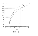
- a measure 6 of the re-entrant region 20 and a measure 0 of a corresponding re-entrant region within the overlying conductor 18 is shown.
- one curve shows the angle 6 of the re-entrant region 20 as a function of the ratio t/h where 't' is the thickness of the dielectric layer 16 deposited over the polysilicon, and 'h' is the thickness of the polysilicon lower level conductor 14 itself.
- the curve has a first span (chain line) corresponding to a polysilicon thickness of about 1 um and a second span (broken line) corresponding to a polysilicon thickness of about 0.4 um.
- a second curve which shows the angle 0 of a corresponding re-entrant region in the upper metallization 18 as is indicated in Figure 4.
- the full line span corresponds to a deposited second conductor layer of thickness 1 to 1.2 um and a first conductor layer of 0.8 to 1 um and the dotted line corresponds to a second conductor layer of 0.8 um and a first conductor layer of 0.4 um.
- the first layer of conductor is polysilicon and the second metal layer is aluminum/silicon alloy.
- the severity of the dielectric re-entrant angle 20 is essentially repeated in the overlying metallization or conducting layer.
- the curves show that although the re-entrant formation 20 is less severe at a ratio of t/h of 2, considerable smoothing of the layer top surface is achieved by extending the ratio to 3 or more.
- the permitted variation from uniform layer thickness is dictated by reliability concerns.
- near-uniformity should be sought to minimize fractures of the metal lines near thinner areas since such fracture leads to open circuits.
- near constricted metal lines a localized increase in current density can generate hot spots with consequent electromigration failures.
- the surface topography of the dielectric layer should ensure that there is no more than a 25% variation in thickness of the second metallization layer.
- the step coverage angles 6 and 0 should be at least 90° so as to preclude any overhang.
- e is usually smaller than ⁇ 1 , it can be fact be 90° while still permitting ⁇ 1 to remain above 90°. and ensuring that the thickness of the second level metallizationdoes not vary by more than 25%.
- circuit design rules must be implemented to ensure that two re-entrant parts associated with a groove between two closely spaced conductor lines do not produce a void. If such a void exists, subsequent etch back may open up the void to create very sharp angle steps.
Landscapes
- Internal Circuitry In Semiconductor Integrated Circuit Devices (AREA)
- Drying Of Semiconductors (AREA)
Applications Claiming Priority (2)
| Application Number | Priority Date | Filing Date | Title |
|---|---|---|---|
| CA456666 | 1984-06-15 | ||
| CA000456666A CA1213075A (fr) | 1984-06-15 | 1984-06-15 | Methode simplifiant les etapes de fabrication des couches dielectriques dans les circuits integres a tres grande echelle |
Publications (2)
| Publication Number | Publication Date |
|---|---|
| EP0164924A2 true EP0164924A2 (fr) | 1985-12-18 |
| EP0164924A3 EP0164924A3 (fr) | 1988-09-07 |
Family
ID=4128106
Family Applications (1)
| Application Number | Title | Priority Date | Filing Date |
|---|---|---|---|
| EP85303445A Withdrawn EP0164924A3 (fr) | 1984-06-15 | 1985-05-16 | Procédé pour améliorer le recouvrement d'une marche par des diélectriques dans les circuits intégrés à très grande échelle |
Country Status (4)
| Country | Link |
|---|---|
| US (1) | US4601781A (fr) |
| EP (1) | EP0164924A3 (fr) |
| JP (1) | JPS6110244A (fr) |
| CA (1) | CA1213075A (fr) |
Families Citing this family (19)
| Publication number | Priority date | Publication date | Assignee | Title |
|---|---|---|---|---|
| DE3421127A1 (de) * | 1984-06-07 | 1985-12-12 | Telefunken electronic GmbH, 7100 Heilbronn | Verfahren zum herstellen einer halbleiteranordnung |
| US5182235A (en) * | 1985-02-20 | 1993-01-26 | Mitsubishi Denki Kabushiki Kaisha | Manufacturing method for a semiconductor device having a bias sputtered insulating film |
| US4667395A (en) * | 1985-03-29 | 1987-05-26 | International Business Machines Corporation | Method for passivating an undercut in semiconductor device preparation |
| US4799992A (en) * | 1985-10-31 | 1989-01-24 | Texas Instruments Incorporated | Interlevel dielectric fabrication process |
| WO1987002828A1 (fr) * | 1985-11-04 | 1987-05-07 | Motorola, Inc. | Dielectrique intermetallique en verre |
| JPS6310544A (ja) * | 1986-07-02 | 1988-01-18 | Oki Electric Ind Co Ltd | 半導体集積回路の製造方法 |
| KR910003742B1 (ko) * | 1986-09-09 | 1991-06-10 | 세미콘덕터 에너지 라보라터리 캄파니 리미티드 | Cvd장치 |
| US5427824A (en) * | 1986-09-09 | 1995-06-27 | Semiconductor Energy Laboratory Co., Ltd. | CVD apparatus |
| US4891247A (en) * | 1986-09-15 | 1990-01-02 | Watkins-Johnson Company | Process for borosilicate glass films for multilevel metallization structures in semiconductor devices |
| US4933743A (en) * | 1989-03-11 | 1990-06-12 | Fairchild Semiconductor Corporation | High performance interconnect system for an integrated circuit |
| JPH02122709U (fr) * | 1989-03-15 | 1990-10-09 | ||
| US5026666A (en) * | 1989-12-28 | 1991-06-25 | At&T Bell Laboratories | Method of making integrated circuits having a planarized dielectric |
| US5089442A (en) * | 1990-09-20 | 1992-02-18 | At&T Bell Laboratories | Silicon dioxide deposition method using a magnetic field and both sputter deposition and plasma-enhanced cvd |
| JP3362397B2 (ja) * | 1991-03-28 | 2003-01-07 | ソニー株式会社 | ポリッシュによる平坦化工程を含む電子装置の製造方法 |
| US5691566A (en) * | 1996-03-25 | 1997-11-25 | Hughes Electronics | Tapered three-wire line vertical connections |
| US6197645B1 (en) | 1997-04-21 | 2001-03-06 | Advanced Micro Devices, Inc. | Method of making an IGFET with elevated source/drain regions in close proximity to gate with sloped sidewalls |
| US6265252B1 (en) | 1999-05-03 | 2001-07-24 | Vlsi Technology, Inc. | Reducing the formation of electrical leakage pathways during manufacture of an electronic device |
| US7347849B2 (en) * | 2001-05-24 | 2008-03-25 | Nxstage Medical, Inc. | Modular medical treatment replaceable component |
| EP1646080B1 (fr) * | 2004-10-07 | 2014-09-24 | Imec | Gravure de structures ayant une haute topographie |
Family Cites Families (5)
| Publication number | Priority date | Publication date | Assignee | Title |
|---|---|---|---|---|
| DE3164742D1 (en) * | 1980-09-22 | 1984-08-16 | Tokyo Shibaura Electric Co | Method of smoothing an insulating layer formed on a semiconductor body |
| JPS5831556A (ja) * | 1981-08-18 | 1983-02-24 | Toshiba Corp | 半導体装置の製造方法 |
| JPS5893353A (ja) * | 1981-11-30 | 1983-06-03 | Nec Corp | 半導体装置の製造方法 |
| JPS5936929A (ja) * | 1982-08-25 | 1984-02-29 | Mitsubishi Electric Corp | 半導体装置の製造方法 |
| JPS5987834A (ja) * | 1982-11-11 | 1984-05-21 | Toshiba Corp | 薄膜形成方法 |
-
1984
- 1984-06-15 CA CA000456666A patent/CA1213075A/fr not_active Expired
- 1984-10-09 US US06/659,145 patent/US4601781A/en not_active Expired - Lifetime
-
1985
- 1985-05-16 EP EP85303445A patent/EP0164924A3/fr not_active Withdrawn
- 1985-06-14 JP JP60128402A patent/JPS6110244A/ja active Pending
Also Published As
| Publication number | Publication date |
|---|---|
| JPS6110244A (ja) | 1986-01-17 |
| US4601781A (en) | 1986-07-22 |
| CA1213075A (fr) | 1986-10-21 |
| EP0164924A3 (fr) | 1988-09-07 |
Similar Documents
| Publication | Publication Date | Title |
|---|---|---|
| US4601781A (en) | Method for improving step coverage of dielectrics in VLSI circuits | |
| US4523975A (en) | Integrated circuit planarizing process | |
| US5795823A (en) | Self aligned via dual damascene | |
| US4980018A (en) | Plasma etching process for refractory metal vias | |
| US5035768A (en) | Novel etch back process for tungsten contact/via filling | |
| US5376435A (en) | Microelectronic interlayer dielectric structure | |
| US7674705B2 (en) | Method of forming a semiconductor device | |
| US4663832A (en) | Method for improving the planarity and passivation in a semiconductor isolation trench arrangement | |
| US6048802A (en) | Selective nonconformal deposition for forming low dielectric insulation between certain conductive lines | |
| US6051880A (en) | Base layer structure covering a hole of decreasing diameter in an insulation layer in a semiconductor device | |
| US4708767A (en) | Method for providing a semiconductor device with planarized contacts | |
| US4666553A (en) | Method for planarizing multilayer semiconductor devices | |
| US6355567B1 (en) | Retrograde openings in thin films | |
| US5094900A (en) | Self-aligned sloped contact | |
| JPH0775235B2 (ja) | シリコンウエハ内に貫通導体を形成する為の平担化方法 | |
| US5514624A (en) | Method of manufacturing a microelectronic interlayer dielectric structure | |
| US6759324B1 (en) | Method of forming a low resistance contact to underlying aluminum interconnect by depositing titanium in a via opening and reacting the titanium with the aluminum | |
| US5567650A (en) | Method of forming tapered plug-filled via in electrical interconnection | |
| US5167760A (en) | Etchback process for tungsten contact/via filling | |
| WO1991010261A1 (fr) | Structure d'interconnexion pour dispositif semiconducteur utilisant un isolateur en polyimide | |
| US5888901A (en) | Multilevel interconnection and method for making | |
| US5399532A (en) | Integrated circuit window etch and planarization | |
| KR100242434B1 (ko) | 반도체 장치의 콘택 형성방법 | |
| EP0405850A2 (fr) | Procédé de formation de diélectriques et composants ainsi produits | |
| WO2002013240A2 (fr) | Procede de formation de lignes d'aluminium sur des trous d'interconnexion remplis d'aluminium dans un substrat semi-conducteur |
Legal Events
| Date | Code | Title | Description |
|---|---|---|---|
| PUAI | Public reference made under article 153(3) epc to a published international application that has entered the european phase |
Free format text: ORIGINAL CODE: 0009012 |
|
| AK | Designated contracting states |
Designated state(s): DE FR GB NL |
|
| PUAL | Search report despatched |
Free format text: ORIGINAL CODE: 0009013 |
|
| AK | Designated contracting states |
Kind code of ref document: A3 Designated state(s): DE FR GB NL |
|
| 17P | Request for examination filed |
Effective date: 19881118 |
|
| 17Q | First examination report despatched |
Effective date: 19901024 |
|
| STAA | Information on the status of an ep patent application or granted ep patent |
Free format text: STATUS: THE APPLICATION IS DEEMED TO BE WITHDRAWN |
|
| 18D | Application deemed to be withdrawn |
Effective date: 19911130 |
|
| RIN1 | Information on inventor provided before grant (corrected) |
Inventor name: MERCIER, JACQUES SERGE Inventor name: HO, VU QUOC |