EP0165604A2 - Appareil d'enregistrement/reproduction comprenant un dispositif de mémoire numérique - Google Patents
Appareil d'enregistrement/reproduction comprenant un dispositif de mémoire numérique Download PDFInfo
- Publication number
- EP0165604A2 EP0165604A2 EP85107597A EP85107597A EP0165604A2 EP 0165604 A2 EP0165604 A2 EP 0165604A2 EP 85107597 A EP85107597 A EP 85107597A EP 85107597 A EP85107597 A EP 85107597A EP 0165604 A2 EP0165604 A2 EP 0165604A2
- Authority
- EP
- European Patent Office
- Prior art keywords
- data
- memory
- audio
- undesirable
- recording
- Prior art date
- Legal status (The legal status is an assumption and is not a legal conclusion. Google has not performed a legal analysis and makes no representation as to the accuracy of the status listed.)
- Withdrawn
Links
Images


Classifications
-
- G—PHYSICS
- G04—HOROLOGY
- G04G—ELECTRONIC TIME-PIECES
- G04G13/00—Producing acoustic time signals
-
- G—PHYSICS
- G06—COMPUTING OR CALCULATING; COUNTING
- G06F—ELECTRIC DIGITAL DATA PROCESSING
- G06F3/00—Input arrangements for transferring data to be processed into a form capable of being handled by the computer; Output arrangements for transferring data from processing unit to output unit, e.g. interface arrangements
- G06F3/16—Sound input; Sound output
Definitions
- the present invention relates to a recording/reproducing apparatus including a digital memory device for recording desirable sound information such as voices in the digital memory device after deleting undesirable sound information from original sound information and for reproducing the recorded desirable sound information in conjunction with the deleted undesirable sound information so as to reproduce the original sound information.
- a magnetic recording tape or a disc are employed for recording voices, music and so on.
- a semiconductor memory of a random access memory (RAM) is utilized as a recording medium to record voice data and music data in a digital form.
- RAM random access memory
- the recording medium is wasted during the recording operation since the appliance is still operated in the recording mode even when no sound information is produced.
- the various attempts have been taken into the electronic appliances having such recording functions.
- cassette tape recorders employ a so-called “automatic shut off” technique that automatically stops the drive motor in response to detection signals indicating no voice input in the recording mode, and automatically commences the recording operation upon receipt of succeeding voice inputs.
- automatic shut off operation although the recording tape is not wasted during the recording mode, it is difficult to completely reproduce the original voice conditions because only the voice information recorded on the tape is reproduced without any processing. That is to say, in the reproducing mode, the tape recorder reproduces such recorded voice information with omitting "no voice" conditions, so that an audience can hardly recognize or imagine the original voice information.
- the object of the present invention may be accomplished by providing a recording/reproducing apparatus including a digital memory device comprising:
- the recording medium it is possible to entirely utilize the recording medium without wasting it in the recording mode when the undesirable sound information occurs and also to reproduce the original sound information containing the undesirable sound information. Further, since the recording and reproducing operations are electrically interrupted during the occurrence of the undesirable sound information, a power consumption can be reduced.
- the particular advantage is obtained in that a relatively large numbers of acoustic command can be digitally recorded in a RAM without using redundant memory regions.
- a recording/reproducing apparatus including a digital memory device in accordance with,the present invention may be realized as various electronic appliances having recording/reproducing functions.
- a great advantage is obtained in that a small electronic timepiece is comprised of a random access memory.
- the present invention is not limited to this embodiment, but can be applied to the other appliances.
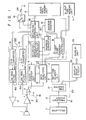
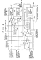
- Fig. 1 shows an electronic timepiece 100 such as a wrist watch, according to one embodiment, including a semiconductor memory for recording and reproducing sound information, e.g., voices and music.
- the electronic timepiece 100 has two functions, i.e., the ordinary time function, and the recording/reproducing function which is electronically communicated with the time function.
- the desirable sound information such as conversation and music is recorded in serial conditions in the RAM after the undesirable sound information, e.g., noises is deleted from the original sound information.
- the recorded desirable sound information is reproduced with the deleted undesirable information superimposed on it, so that the original sound information is ultimately reproduced.
- An acoustic converter 1 is provided as a microphone in the recording mode and a speaker in the reproducing mode. Audio information, e.g., voice or music is first converted into an audio signal. The audio signal is amplified in a recording amplifier 2 to a given signal level, and then the amplified signal is supplied to a negative input terminal of a comparator 3. To a positive input terminal of this comparator 3 a reference voltage Vr is being applied from a DC source 50. An output signal of the comparator 3, as described hereinafter, is supplied to a silent time counter unit 5. The output represents whether levels of the audio signal derived from the amplifier 2 exceed the reference voltage level.
- An oscillator 7 oscillates a signal in a given frequency.
- the signal is frequency-divided into a predetermined clock signal by a frequency divider 8.
- the clock signal has two frequency components of ⁇ 1 and ⁇ 0 .
- the former signal ⁇ 1 is used as a sampling signal.
- the latter clock signal ⁇ 0 is supplied to the silent - time counter unit 5 and the data analyzing unit 6 respectively.
- the silent time counter unit 5 measures the silent time, i.e., no audio signal by counting the clock signal ⁇ 0 .
- the silent time information is given from the comparator outputs.
- the resultant data i.e., the silent time
- the data analyzing unit 6 receives set time data from a set time memory unit 9. Also another time is preset by an external switch (not shown). When the measured silent time is longer than the preset set time of the set time memory unit 9, time difference data "A" and discrimination signals "J O " and "J l " are derived as undesirable audio time data from the data analyzing unit 6.
- the time difference data "A” is transferred via a silent time memory controller 10 to a silent time memory unit 11 where it is stored under the control of the silent time memory controller 10.
- Another function of the silent time memory controller 10 is to control reproduction operations, data of which have been stored in a digital form in the silent time memory unit 11.
- a pushbotton switch SW is provided as an operation mode selector.
- the pushbotton switch SW is connected to a trigger terminal T of a triggerable flip-flop (T-FF) 13.
- T-FF triggerable flip-flop
- the switching conditions of the mode selector switch SW are inverted in the flip-flop 13.
- mode designation signals for the recording and reproducing modes are supplied to a recording/reproducing unit 14.
- the recording mode or the reproducing mode is selected by the recording/reproducing unit 14.
- the analogue aural signal derived from the amplifier 2 is filtered in a low pass filter 15a and then converted into a digital aural data by an analogue- to-digital (A/D) converter 15b.
- A/D analogue- to-digital
- the digital audio data is supplied to the recording/reproducing unit 14.
- the low pass filter 15a and the A/D converter 15b constitute an A/D conversion unit 15.
- the digital audio data is sequentially stored in an audio data memory unit 12, as described in detail hereinafter.
- the reproducing mode is selected by the selector switch SW, the digital audio data is sequentially read out from the audio data memory unit 12, and D/A-converted by a D/A converter 16b into the corresponding analogue audio signal.
- the analogue audio signal is further processed in a low pass filter 16a and an amplifier 17.
- the amplified audio signal is converted in the acoustic converter 1 into the original acoustic information as described in detail hereinafter.
- one control signal of a recording/reproducing controller 20 is supplied to the recording/reproducing unit 14.
- the recording/reproducing controller 20 causes the recording operation of the recording/reproducing unit 14 to be interrupted upon receipt of one analysis or discrimination signal "J O ".
- the analysis signal "J O " is produced from the data analyzing unit 6 in a case that the measured silent time is longer than the preset time of the set time memory unit 9.
- the recording/reproducing controller 20 interrupts the reproducing operation of the recording/reproducing unit 14 when the time difference data is read out from the silent time memory unit 11.
- a time clock signal of 1 Hz is produced from the frequency divider 8 to be sent to a time counter 21.
- the time and date data are obtained in the time counter 21 by counting the time clock signal.
- The. time and date data are sent to a display drive circuit 22 in which they are converted into display data. This display data is further sent to a display unit 23 to be opto- electronically displayed.
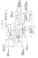
- Fig. 2 is an internal circuit diagram of the data analyzing unit 6 in connection with the silent time counter unit 5 and the set time memory unit 9.
- the output signal Y of the comparator 3 is supplied to one input of an AND gate 5a and the clock signal of the frequency divider 8 is supplied to the other input of the AND gate 5a.
- An output of this AND gate 5a is supplied to a counter 5b.
- the comparator output Y is also supplied via an inverter 5c to a reset terminal of the counter 5b.
- the comparator output Y is supplied via an AND gate 6a to a rising edge detector 6b.
- An output pulse signal "J o " of the rising edge detector 6b is supplied to a reset terminal of a flip-flop 6c and to an arithmetic operation circuit 6d as an operation command signal, and is derived from the data analyzing unit 6.
- the arithmetic operation circuit 6d calculates a difference between the output of the counter 5b and the output of the set time memory unit 9, i.e., the preset time.
- a coincidence detector 6e of the data analyzing unit 6 receives the output of the counter 5b and the preset time of the set time memory unit 9. As a consequence, the detector 6e detects the data coincidence of these inputs in synchronism with the clock signal ⁇ 0 . The coincidence signal is then supplied to the set terminal of the flip-flop 6c. From the set output Q of this flip-flop 6c, an output or discrimination signal "Ji" is derived and also supplied to the AND gate 6a.
- the first discrimination signal "J I " is the coincidence signal produced when the measured silent time reaches the set time
- the second discrimination signal "J o " is the rising-edge detection signal produced when the succeeding audio signal is detected.
- Fig. 3 is an internal circuit diagram of the recording/reproducing unit 14 and its relevant units 10 and 20.
- the output signal of the output terminal Q of the mode selecting flip-flop 13 is supplied to a rising edge detector 14a for the recording mode of the recording/reproducing unit 14.
- An output of the rising edge detector 14a is supplied to a set terminal S of a flip-flop 14b.
- An output of an output terminal Q of the flip-flop 14b is supplied as an operation command signal to the amplifier 2 and the A/D converter unit 15, and supplied via an OR gate 14c to one input terminal of an AND gate 14d.
- an output of an AND gate 14e is supplied to other input terminal of the AND gate 14d.
- This AND gate 14e has two input terminals; one receiving the sampling signal ⁇ 1 of the frequency divider 8 and the other receiving an output of an inverter 20a of the recording/reproducing controller 20.
- the output of the output terminal Q of the mode selecting flip-flop 13 is sent to a rising edge detector 14h for the reproducing mode.
- An output of the rising edge detector 14h is delivered to a set terminal S of a flip-flop 14i.
- An output of the flip-flop 14i is supplied as a reproduction command signal to the amplifier 17 and the D/A converter unit 16, and also supplied to an OR gate 14c, so that the sampling pulse ⁇ 1 is counted in the address counter 14g.
- the audio data sequentially read out from the audio data memory unit 12 can be transferred through the above gate circuit G I to the D/A converter unit 16.
- the audio information is reproduced from the acoustic converter 1.
- the discrimination signal "J l " derived from the data analyzing unit 6 is sent via an inverter 20a to an OR gate 20b, and via an OR gate 18b to the address counter 18 as a logic 1-level signal.
- the other discrimination signal “J O " is supplied through an inverter 12a to the audio data memory unit 12.
- This signal "J 0 " is supplied to gate circuits G 2 and G 3 of the silent time memory controller 10 so as to open these gate circuits G 2 and G 3 , and also supplied as a destination signal to the address converter 19.
- the silent time data read out from the silent time memory unit 11 is preset via the gate circuit G 4 into a subtraction timer 10a of the silent time memory controller 10.
- This gate circuit G 4 is opened by an output of the inverter 12a into which 1-bit data is input from the audio data memory unit 12. While a certain counting number is still present in this subtraction timer 10a, a logic 1-level signal is output from a pulse number detector 10b to the OR gate 20b of the recording/reproducing controller 20.
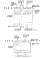
- Fig. 4 the memory format and the relative input/output data for the audio data memory unit 12 are depicted and in Fig. 5, those for the silent time memory unit 11 are shown.
- the audio data memory unit 12 is divided into three regions, i.e., an address number region, an audio data code region and an audio data region.
- a voice code "I” or a no voice code "0" is stored in accordance with the address numbers 0001 , 0002 , --- 1111 , these codes being sent via the inverter 12a from the data analyzing unit 6.
- the audio data #1, #2 or the 8-bit address data of the silent time memory unit 11, e.g., 00000001 is stored respectively.
- the address region corresponding to the voice code "1" stores the audio data
- one corresponding to the no voice code "0" stores the address data corresponding to the read address for the silent time memory unit 11 when the silent time data is stored in the silent time memory unit 11 (as described in detail hereinafter).
- the corresponding silent time data is stored in 8-bit data, e.g., 00000111 . It is to be understood that the address number of the silent time memory unit 11 is 4-bit data, and this 4-bit data is converted into 8-bit data in the address converter 19 for the address number of the audio data memory unit 12.
- the switch SW is operated to derive the output signal from the output terminal Q of the flip-flop 13.
- the rising edge of the output signal is detected in the rising edge detector 14a, so that the following flip-flop 14b is set (see Fig. 3).
- the amplifier 2 and the A/D converter unit 15 are in operation.
- this audio signal is supplied to one input of the comparator 3.
- the reference voltage Vr is being applied to the other input of the comparator 3.
- a logic 1-level signal is produced from the comparator 3.
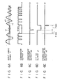
- the comparator 3 outputs a rectangular waveform Y as shown in Fig. 6B.
- the 1-level signal represents the audio signal components such as voice or music
- the 0-level signal indicates no signal component, or smaller signal components than the given range ⁇ a, e.g., noise components or no voice condition.
- the comparator output Y is pulse-width-modulated in the comparator 3, the width thereof represents the amplitude of the audio signal components or the duration time (for instance 10 seconds) of no signal component.
- the audio signal in the logic level derived from the comparator 3 is supplied to the silent time counter unit 5 and the data analyzing unit 6 respectively.
- the content of the counter unit 5 is reset when the level of the input audio logic signal is changed from “0" to “1”, and it starts the counting operation when the logic level is changed from “1” to "0". Since the silent time counter unit 5 performs its counting operations in accordance with the comparator's output signals i.e., the logic levels, the counted data corresponds to the silent time, e.g., 10 seconds in the present embodiment.
- the data analyzing unit 6 effects its comparison on both the input data every clock signal $ 0 .
- the counting time of the counter unit 5 does not yet reach the set time of the set time memory unit 9, the discrimination signals "Jo" and "J 1 " remain “0” levels.
- the silent time the counted values of the silent time counter unit 5
- the set time e.g., 3 seconds
- the recording/reproducing unit 14 performs the following write-in operation.
- the sequentially transferred groups of the audio data are successively written into the designated memory regions of the audio data memory unit 12 by designating the memory address from the top address to the bottom address. Accordingly, while the input silent time (i.e., the counted value) is shorter than the predetermined set time (e.g., 3 seconds) that is judged by the data analyzing unit 6, the acoustic information received by the acoustic converter 1 is recorded in a digital form in the audio memory unit 12 according to the normal recording process. Therefore, the recorded audio data (acoustic information) is recognized as the desirable audio data. It is understood that both the discrimination signals "Jo" and "J l " remain "zero(0)" during such a normal recording operation.
- the output (coincidence signal) of the coincidence detector 6e can set the followed flip-flop 6c so that one discrimination signal "J l " becomes "1" (see Figs. 6C and 6D).
- the inverter 20a of the recording/reproducing controller 20 derives a "0" level signal, the gate circuit GO is closed, and simultaneously no sampling pulse ⁇ 1 is produced from the AND gate 14e. This causes the recording/reproducing unit 14 to be nonoperative. Thus, the recording operation is interrupted.
- the silent time memory controller 10 Upon receipt of the other discrimination signal "J O " the silent time memory controller 10 enables the gate circuits G 2 and G 3 to be opened (Fig. 3). Addresses for the silent time memory unit 11 are designated depending upon the contents of the memory address counter 18. Consequently, the above 8-bit silent time data is written as the undesirable audio time data in the designated memory region under the control of the silent time memory controller 10 (see Fig. 7).
- the memory address converter 19 converts the 4-bit address data stored in the address counter 18 into the 8-bit address data. The resultant 8-bit address data corresponding to the above silent time data is transferred to the recording/reproducing unit 14 as the recording data on the silent time.
- the contents of the address counter are counted up by (+1), while the output ("0" level signal due to the discriminating signal "J 1 ") of the inverter 12a and also the contents of the address counter 18 fed through the address converter 19 are stored in the memory regions of the audio data unit 12 designated by the address counter 14g.
- the silent time data is stored in the silent time memory unit 11, and both the audio data and the memory address indicating the silent time data are stored in the separate memory unit 12. That is, since only the audio data (desirable acoustic information) and the memory address representing silent time data are stored in the audio data memory unit 12, the memory capacity thereof can be considerably saved for the silent time data.
- the contents of the address counter 18 is counted up by (+1) in response to the output of the inverter 12b (see Fig. 4).
- the silent time data is read out from the silent time memory unit 11 and thereafter preset into the subtraction timer 10a.
- the pulse number detector 10b outputs its detection signal to the OR gate 20b of the recording/reproducing controller 20, the signal level of the inverter 20a becomes "0", so that the count-up operation of the address counter 14g is interrupted (see Figs. 3 and 5).
- the reproducing operation is.interrupted while the silent time data is processed, with the result that the silent time occurred in the input acoustic information can be completely reproduced in conjunction with the desirable acoustic information.
- Fig. 7 schematically shows another memory format of the audio data memory unit 12.
- the silent time data was stored in the silent time memory unit 11 different from the audio data memory unit 12.
- the present invention is not restricted to the above example.
- Fig. 8 is a schematic diagram of another recording/reproducing unit 80 according to the invention.
- the same reference numerals of the circuit elements in the previous unit 14 shown in Fig. 3 are used for the same or similar circuit elements in this unit 80.
- the output Q of the flip-flop 14b at the output side of the rising edge detector 14a is supplied to one input terminal of the AND gate 14j, while the other input, terminal of the AND gate 14j receives a signal having 1 Hz which is a time clock signal of the frequency divider 8.
- the outputs of the AND gate 14j are counted by the recording counter 14k.
- the resultant data of this recording counter 14 together with the contents of the address counter 14g are sent to the display drive unit 22 so as to display these data in the display unit 23.
- the recording/reproducing apparatus including the digital memory device according to the present invention may be applied to a so-called "data bank" in which various kinds of data such as telephone numbers, addresses, and names can be stored in the digital memory device.
Landscapes
- Engineering & Computer Science (AREA)
- Physics & Mathematics (AREA)
- General Physics & Mathematics (AREA)
- Theoretical Computer Science (AREA)
- Health & Medical Sciences (AREA)
- Audiology, Speech & Language Pathology (AREA)
- General Health & Medical Sciences (AREA)
- Human Computer Interaction (AREA)
- General Engineering & Computer Science (AREA)
- Signal Processing For Digital Recording And Reproducing (AREA)
- Signal Processing Not Specific To The Method Of Recording And Reproducing (AREA)
- Indexing, Searching, Synchronizing, And The Amount Of Synchronization Travel Of Record Carriers (AREA)
Applications Claiming Priority (2)
| Application Number | Priority Date | Filing Date | Title |
|---|---|---|---|
| JP90891/84U | 1984-06-20 | ||
| JP9089184U JPS616923U (ja) | 1984-06-20 | 1984-06-20 | 録音機能付小型電子機器 |
Publications (2)
| Publication Number | Publication Date |
|---|---|
| EP0165604A2 true EP0165604A2 (fr) | 1985-12-27 |
| EP0165604A3 EP0165604A3 (fr) | 1986-02-05 |
Family
ID=14011033
Family Applications (1)
| Application Number | Title | Priority Date | Filing Date |
|---|---|---|---|
| EP85107597A Withdrawn EP0165604A3 (fr) | 1984-06-20 | 1985-06-19 | Appareil d'enregistrement/reproduction comprenant un dispositif de mémoire numérique |
Country Status (2)
| Country | Link |
|---|---|
| EP (1) | EP0165604A3 (fr) |
| JP (1) | JPS616923U (fr) |
Cited By (2)
| Publication number | Priority date | Publication date | Assignee | Title |
|---|---|---|---|---|
| GB2253078A (en) * | 1991-02-21 | 1992-08-26 | Radamec Group Plc | Apparatus for the storage and playback of spoken messages |
| GB2305750A (en) * | 1995-09-30 | 1997-04-16 | Samsung Electronics Co Ltd | Recording audio to IC card with silence detection |
Family Cites Families (3)
| Publication number | Priority date | Publication date | Assignee | Title |
|---|---|---|---|---|
| US3641500A (en) * | 1970-06-30 | 1972-02-08 | Ibm | Voice entry system |
| GB2063528B (en) * | 1979-09-27 | 1983-05-11 | Casio Computer Co Ltd | Electronic timepiece |
| US4376874A (en) * | 1980-12-15 | 1983-03-15 | Sperry Corporation | Real time speech compaction/relay with silence detection |
-
1984
- 1984-06-20 JP JP9089184U patent/JPS616923U/ja active Pending
-
1985
- 1985-06-19 EP EP85107597A patent/EP0165604A3/fr not_active Withdrawn
Cited By (4)
| Publication number | Priority date | Publication date | Assignee | Title |
|---|---|---|---|---|
| GB2253078A (en) * | 1991-02-21 | 1992-08-26 | Radamec Group Plc | Apparatus for the storage and playback of spoken messages |
| GB2305750A (en) * | 1995-09-30 | 1997-04-16 | Samsung Electronics Co Ltd | Recording audio to IC card with silence detection |
| GB2305750B (en) * | 1995-09-30 | 1998-02-18 | Samsung Electronics Co Ltd | Recording method and apparatus of an audio signal using an integrated circuit memory card |
| US5754979A (en) * | 1995-09-30 | 1998-05-19 | Samsung Electronics Co., Ltd. | Recording method and apparatus of an audio signal using an integrated circuit memory card |
Also Published As
| Publication number | Publication date |
|---|---|
| JPS616923U (ja) | 1986-01-16 |
| EP0165604A3 (fr) | 1986-02-05 |
Similar Documents
| Publication | Publication Date | Title |
|---|---|---|
| US5014317A (en) | Recording/reproducing apparatus with voice recognition function | |
| CA2054880A1 (fr) | Dispositif d'enregistrement et de lecture d'informations | |
| JPS6238179B2 (fr) | ||
| US4508457A (en) | Electronic timepiece with record/playback circuits | |
| US5173888A (en) | Playback system for audio memory disks | |
| EP0165604A2 (fr) | Appareil d'enregistrement/reproduction comprenant un dispositif de mémoire numérique | |
| KR900003837A (ko) | 음성 메세지 기억 회로 및 이를 위한 마이콤 제어 방법 | |
| JPH0341322Y2 (fr) | ||
| US5499317A (en) | Audio message storing circuit and control method therefor | |
| JPH0535510B2 (fr) | ||
| JP2605663B2 (ja) | 録音機能付電子機器 | |
| JPH0526594Y2 (fr) | ||
| JP3416340B2 (ja) | ビデオテープレコーダ | |
| JPH0532860Y2 (fr) | ||
| KR0117510Y1 (ko) | 멀티디스크재생시스템의 디스크판별장치(apparatus for disc distinction in multi-disc reproducing system) | |
| JPS5850608A (ja) | 音響信号の再生装置 | |
| KR930003175B1 (ko) | 디지틀 신호재생및 녹음장치 | |
| KR910002024B1 (ko) | 음성 축적장치 | |
| JPS635039Y2 (fr) | ||
| KR100229536B1 (ko) | 브이씨알의 오디오 신호 디지털 처리 방법 | |
| JPH059737Y2 (fr) | ||
| JPS61163394A (ja) | 音声発生装置 | |
| JPS59216195A (ja) | 音声処理方式 | |
| JPH0632038B2 (ja) | 電子式録音装置 | |
| JPS6166260A (ja) | サンプリング周波数切換装置 |
Legal Events
| Date | Code | Title | Description |
|---|---|---|---|
| PUAI | Public reference made under article 153(3) epc to a published international application that has entered the european phase |
Free format text: ORIGINAL CODE: 0009012 |
|
| PUAL | Search report despatched |
Free format text: ORIGINAL CODE: 0009013 |
|
| AK | Designated contracting states |
Designated state(s): CH DE FR GB LI |
|
| AK | Designated contracting states |
Designated state(s): CH DE FR GB LI |
|
| 17P | Request for examination filed |
Effective date: 19860708 |
|
| 17Q | First examination report despatched |
Effective date: 19880728 |
|
| STAA | Information on the status of an ep patent application or granted ep patent |
Free format text: STATUS: THE APPLICATION IS DEEMED TO BE WITHDRAWN |
|
| 18D | Application deemed to be withdrawn |
Effective date: 19881208 |
|
| RIN1 | Information on inventor provided before grant (corrected) |
Inventor name: FUJII, HIROSHI |