EP0165766B1 - Circuit filtre intégré - Google Patents
Circuit filtre intégré Download PDFInfo
- Publication number
- EP0165766B1 EP0165766B1 EP85304174A EP85304174A EP0165766B1 EP 0165766 B1 EP0165766 B1 EP 0165766B1 EP 85304174 A EP85304174 A EP 85304174A EP 85304174 A EP85304174 A EP 85304174A EP 0165766 B1 EP0165766 B1 EP 0165766B1
- Authority
- EP
- European Patent Office
- Prior art keywords
- conductive plate
- resistor
- resistors
- filter
- capacitor
- Prior art date
- Legal status (The legal status is an assumption and is not a legal conclusion. Google has not performed a legal analysis and makes no representation as to the accuracy of the status listed.)
- Expired
Links
Images

Classifications
-
- H—ELECTRICITY
- H03—ELECTRONIC CIRCUITRY
- H03H—IMPEDANCE NETWORKS, e.g. RESONANT CIRCUITS; RESONATORS
- H03H11/00—Networks using active elements
- H03H11/02—Multiple-port networks
- H03H11/04—Frequency selective two-port networks
- H03H11/0405—Non-linear filters
-
- H—ELECTRICITY
- H10—SEMICONDUCTOR DEVICES; ELECTRIC SOLID-STATE DEVICES NOT OTHERWISE PROVIDED FOR
- H10D—INORGANIC ELECTRIC SEMICONDUCTOR DEVICES
- H10D84/00—Integrated devices formed in or on semiconductor substrates that comprise only semiconducting layers, e.g. on Si wafers or on GaAs-on-Si wafers
- H10D84/201—Integrated devices formed in or on semiconductor substrates that comprise only semiconducting layers, e.g. on Si wafers or on GaAs-on-Si wafers characterised by the integration of only components covered by H10D1/00 or H10D8/00, e.g. RLC circuits
- H10D84/204—Integrated devices formed in or on semiconductor substrates that comprise only semiconducting layers, e.g. on Si wafers or on GaAs-on-Si wafers characterised by the integration of only components covered by H10D1/00 or H10D8/00, e.g. RLC circuits of combinations of diodes or capacitors or resistors
- H10D84/206—Integrated devices formed in or on semiconductor substrates that comprise only semiconducting layers, e.g. on Si wafers or on GaAs-on-Si wafers characterised by the integration of only components covered by H10D1/00 or H10D8/00, e.g. RLC circuits of combinations of diodes or capacitors or resistors of combinations of capacitors and resistors
-
- H—ELECTRICITY
- H10—SEMICONDUCTOR DEVICES; ELECTRIC SOLID-STATE DEVICES NOT OTHERWISE PROVIDED FOR
- H10D—INORGANIC ELECTRIC SEMICONDUCTOR DEVICES
- H10D88/00—Three-dimensional [3D] integrated devices
Definitions
- This invention relates to the design and structure of electronic filters, and more particularly to an electronic filter which can be implemented in an integrated circuit having a substantially reduced die area as compared with prior art filters.
- Filters are well known in the prior art. Such filters serve as means for rejecting signals above a selected frequency (low pass filter), rejecting signals below a selected frequency (high pass filter), rejecting signals of a selected frequency (notch filter), or rejecting frequencies other than those within a predefined frequency range (band pass filter). Oftentimes, it is desirable to sample an analog signal; for example, for use in a sampled data system. Such sampled data systems are widespread and provide the advantages of allowing a digital circuit to perform analog functions. One of the problems associated with such sampled systems is known as "aliasing". Aliasing is the undesired effect that, in addition to passing selected frequencies within its desired pass band, a sampled data system will pass signals having a frequency near the sampling frequency.
- Figure 1 illustrates this aspect of aliasing.
- Fig. 1 shows a frequency domain graph of a sampled data system in which it is desired to pass audio signals within the frequency range of 0-3 kHz.
- the filter characteristics are such as are shown on the left-hand side of Fig. 1.
- the sampled data rate is 128 kHz
- the same transfer function is provided on both sides of 128 kHz.
- signals within the range of 128 ⁇ 3 kHz are passed by the sampled data system.
- these signals appear at the base band by virtue of being "mixed" with the 128 kHz clock frequency. It is therefore desirable to eliminate the presence of such high frequency signals prior to being fed to the sampled data system.
- a low pass prefilter or "antialiasing filter”
- the graph of the transfer function of a typical antialiasing filter is shown superimposed on the graph of Fig. 1.
- Antialiasing filters are well known in the prior art and typically comprise a simple low pass filter. In many instances, a fair amount of attenuation is desired, and thus a two-pole filter is utilized.
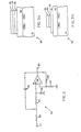
- One such two-pole filter is shown in the schematic diagram of Figure 2.
- Antialiasing filter 20 includes operational amplifier 26 having its inverting input terminal connected through resistor 27 to ground and also through resistor 28 to output terminal 29. The noninverting input terminal of operational amplifier 26 is connected through capacitor 25 to ground and through resistor 23 and resistor 22 to input terminal 21. The node between resistors 22 and 23 is connected through capacitor 24 to the output terminal of operational amplifier 26.
- the transfer function for the two-pole low pass filter 20 is as follows: where where where
- resistors 22, 23, 27 and 28 and capacitors 24 and 25 are selected by well-known principles, such as are stated in "Rapid Practical Design of Active Filters” by D. E. Johnson and J. L. Hilburn, John Wiley & Son, (particularly pages 12, 13 and 27-29), which is hereby incorporated by reference.
- Prior art techniques for fabricating such antialiasing filters utilize portions of the polycrystalline silicon interconnect layer as resistors 22, 23, 27 and 28. While the use of polycrystalline silicon resistors is well known, and easily implemented in order to fabricate the antialiasing filter 20 of Fig. 2, the use of polycrystalline silicon resistors requires a substantial amount of die area. Polycrystalline silicon resistors typically have a resistance of approximately 20 ohms per square. Typically resistor values needed are within the range of approximately 50 kO to 400 kO. Using polycrystalline silicon requires a large number of squares (for example, 1 square of polycrystalline silicon may be designed to be 8 microns square); further, resistors are spaced at least 5 microns apart and thus require a large area.
- Table 1 shows an approximate area calculation for a voice band filter having a closed loop gain of unity.
- the prior art antialiasing filter 20 of Fig. 2 fabricated on an integrated circuit device utilizing prior art techniques including the use of polycrystalline silicon resistors, and allowing approximately 10% additional area for proper spacing and interconnection, requires approximately 1730 sq. mils per antialiasing filter.
- This is a substantial amount of integrated circuit device area, and substantially limits the number of integrated circuits which may be formed on a single semiconductor wafer.
- the smaller the die area required for an integrated circuit the more integrated circuits may be fit onto a single semiconductor wafer, and the greater number of finished integrated circuits possible for a given amount of semiconductor processing. This, of course, decreases the cost of each finished integrated circuit device.
- a semiconductor element having a substrate with a channel zone which may act as a resistor with distributed capacitance to an overlying gate electrode and to the substrate is described in GB-A-2077 496.
- a semiconductor structure including a substrate of a first conductivity type, a resistor formed within the substrate, the resistor being lightly doped to a second conductivity type opposite to the first conductivity type and a first conductive plate formed above and insulated from the resistor, wherein the first conductive plate is intended for coupling to a fixed voltage to shield the underlying resistor, characterised by a second conductive plate formed above and insulated from the first conductive plate, the first and second conductive plates forming a capacitor.
- a method for forming a semiconductor structure including the steps of forming within a semiconductor substrate of a first conductivity type a resistor being lightly doped to a second conductivity type opposite to the first conductivity type, forming a first insulation layer over the semiconductor substrate, and forming a first conductive plate on the first insulation layer above the resistor, wherein the first conductive plate is intended for coupling to a fixed voltage to shield the underlying resistor, characterised by including the steps of forming a second insulation layer on the first conductive plate and forming a second conductive plate on the second insulation layer.
- an integrated circuit filter in a semiconductor body including an operation amplifier, a capacitor, and a resistor, wherein the resistor is formed as a lightly doped region within the semiconductor body and the capacitor is formed by a first conductive plate and a second conductive plate wherein the first conductive plate is formed above and insulated from the resistor so that when a fixed voltage is coupled to the first conductive plate the plate will shield the underlying resistor, characterised in that the second conductive plate is formed above and insulated from the first conductive plate.
- an electronic filter which has particular application for use as an antialiasing filter in sampled data systems.
- the filter of this invention is fabricated so as to utilize high resistivity diffused regions within the semiconductor body, as opposed to low resistivity polycrystalline silicon resistors.
- the values of the resistor and capacitor will be such that the high resistivity resistor requires a small amount of space, and is physically located under the lower plate of the capacitor used in the filter of this invention.
- the lower plate of the capacitor is intended to be connected to a fixed voltage potential, thereby in effect shielding the underlying resistor from the deleterious effect of changes in voltage, and thus preventing the modulation of the resistance value of the resistors located beneath the capacitor. In this manner, the resistance value is highly constant.
- Figure 3a is a cross-sectional view of the resistors and capacitors formed in accordance with the teachings of this invention in order to fabricate a filter in accordance with the teachings of this invention.
- Figure 3b is a cross-sectional view of another embodiment of the resistors and capacitors utilized in accordance with the teachings of this invention.
- a filter is designed in such a manner that the resistors required are fabricated of relatively high resistivity diffused areas within a semiconductor body, rather than the relatively low resistivity polycrystalline silicon resistors utilized in the prior art or relatively low resistivity diffused resistors utilized in the prior art.
- polycrystalline silicon resistors typically have a resistance of approximately 20 ohms per square, which is significantly less than the resistivity of the high resistivity diffused regions utilized as resistors in accordance with the teachings of this invention, which have resistivities of approximately 2000 ohms per square. Accordingly, the use of such higher resistivity resistors allows an integrated circuit areas savings for the formation of resistors of approximately 100-fold.
- resistors of diffused regions having relatively high resistivities within a semiconductor body it is also contemplated that this may be accomplished without the need for additional masking or doping steps.
- well regions are formed having relatively high resistivites.
- the high resistivity resistors fabricated in accordance with the teachings of this invention are fabricated simultaneously with the fabrication of such well regions, thereby not requiring any additional masking or doping steps.
- the resistance values themselves and the capacitance values are selected such that the resistors may be located in the area beneath the capacitors.
- the resistors may be located in the area beneath the capacitors.
- a significant saving in die area is achieved.
- FIG. 3a the cross-sectional view of a portion of an integrated circuit including resistor diffusions 36 and 37 is shown beneath the capacitor formed of plates 33 and 35 and interplate dielectric layer 34.
- Resistors 36 and 37 are insulated from plate 33 by insulation layer 32, which in one embodiment is field oxide having a thickness on the order of 10,000 A.
- resistor diffusions 36 and 37 are used to provide electrical interconnection to resistor diffusions 36 and 37. These portions of rseistor diffusions 36 and 37 can, if desired, extend out from beneath capacitor plate 33 to provide easy electrical connection to other circuit elements (not shown).
- the lower plate 33 is connected to ground (or any other suitable constant voltage) in order to effectively shield the resistance diffusions 36 and 37 from the undesirable effect of changing voltage levels.
- ground or any other suitable constant voltage
- the resistance of a lightly doped diffused region varies depending upon the voltages impressed upon it.
- diffused resistance regions 36 and 37 are not influenced by various voltages in the integrated circuit device, and thus exhibit highly constant resistance values. This is particularly important because, if the resistor values are not constant, their resistance values are not linear with voltage and current, they may serve as multipliers and in effect provide harmonics of the signals passing through them.
- the lower plate 33 of the capacitor shown in Fig. 3a corresponds to the lower plate of capacitor 25 shown in Figure 2, which is connected to ground.
- the resistance and capacitance values of the filter be selected such that the resistors may be fabricated beneath the capacitors and, preferably, that the resistors be fabricated beneath only those capacitors in the filter having their lower plate connected to ground or a fixed voltage level.
- the lower plate be expanded in area in order to cover the underlying resistors. This is depicted in Fig. 3b in which the lower plate 43 of the capacitor, which is connected to ground or a suitable reference voltage, is significantly larger than the upper plate 45. While the added area of lower plate 43 has minimal effect on the capacitance value of the capacitor, it has great effect in shielding the underlying resistors.
- a plate having a substantially fixed voltage impressed thereon is formed over and insulated from underlying diffused resistors in order to shield those resistors from spurious voltages created in other parts of the circuit.
- the low pass antialiasing filter of Fig. 2 was constructed having substantially the same transfer characteristic as in the priorart example set out in Table 1. However, the resistance values of resistors 22, 23, 27 and 28 were selected such that they conveniently are located beneath the lower plate of capacitor 25.
- the resistance and capacitance values and sizes are given as shown below in Table 2, where the resistances of resistors 27 and 28 are selected such that the closed loop gain of operational amplifier 26 is unity.
- the resistance and capacitance values and sizes in an alternative embodiment of this invention, where the resistances of resistors 27 and 28 are selected such that the closed loop gain of operational amplifier 26 is equal to four, is shown in Table 3.
- filters fabricated in accordance with the teachings of this invention are fabricated utilizing significantly less integrated circuit die area than comparable filters constructed in accordance with prior art techniques.
- the term "lightly doped” refers to a semiconductor region which is doped to an extent which is appropriate for the formation of a diffused resistor and is low relative to the doping levels of doped regions commonly used in other types of semiconductor devices.
Landscapes
- Physics & Mathematics (AREA)
- Nonlinear Science (AREA)
- Semiconductor Integrated Circuits (AREA)
- Networks Using Active Elements (AREA)
Claims (6)
Applications Claiming Priority (2)
| Application Number | Priority Date | Filing Date | Title |
|---|---|---|---|
| US62241484A | 1984-06-20 | 1984-06-20 | |
| US622414 | 1984-06-20 |
Publications (2)
| Publication Number | Publication Date |
|---|---|
| EP0165766A1 EP0165766A1 (fr) | 1985-12-27 |
| EP0165766B1 true EP0165766B1 (fr) | 1989-08-30 |
Family
ID=24494085
Family Applications (1)
| Application Number | Title | Priority Date | Filing Date |
|---|---|---|---|
| EP85304174A Expired EP0165766B1 (fr) | 1984-06-20 | 1985-06-12 | Circuit filtre intégré |
Country Status (4)
| Country | Link |
|---|---|
| EP (1) | EP0165766B1 (fr) |
| JP (1) | JPH0693487B2 (fr) |
| CA (1) | CA1228175A (fr) |
| DE (1) | DE3572751D1 (fr) |
Families Citing this family (2)
| Publication number | Priority date | Publication date | Assignee | Title |
|---|---|---|---|---|
| FR2597278A1 (fr) * | 1986-04-11 | 1987-10-16 | Efcis | Cellule de filtrage passe-bas pour circuit integre |
| US4853759A (en) * | 1986-09-29 | 1989-08-01 | American Microsystems, Inc. | Integrated circuit filter with reduced die area |
Family Cites Families (4)
| Publication number | Priority date | Publication date | Assignee | Title |
|---|---|---|---|---|
| JPS5810863B2 (ja) * | 1978-04-24 | 1983-02-28 | 株式会社日立製作所 | 半導体装置 |
| JPS5593252A (en) * | 1979-01-05 | 1980-07-15 | Mitsubishi Electric Corp | Substrate potential generating apparatus |
| US4399417A (en) * | 1980-06-06 | 1983-08-16 | Bell Telephone Laboratories, Incorporated | Integrated CRC filter circuit |
| JPS5870566A (ja) * | 1981-10-23 | 1983-04-27 | Hitachi Ltd | 半導体装置 |
-
1985
- 1985-05-14 CA CA000481462A patent/CA1228175A/fr not_active Expired
- 1985-06-03 JP JP60118991A patent/JPH0693487B2/ja not_active Expired - Lifetime
- 1985-06-12 DE DE8585304174T patent/DE3572751D1/de not_active Expired
- 1985-06-12 EP EP85304174A patent/EP0165766B1/fr not_active Expired
Also Published As
| Publication number | Publication date |
|---|---|
| DE3572751D1 (en) | 1989-10-05 |
| JPH0693487B2 (ja) | 1994-11-16 |
| EP0165766A1 (fr) | 1985-12-27 |
| JPS618967A (ja) | 1986-01-16 |
| CA1228175A (fr) | 1987-10-13 |
Similar Documents
| Publication | Publication Date | Title |
|---|---|---|
| US5514612A (en) | Method of making a semiconductor device with integrated RC network and schottky diode | |
| US7262681B2 (en) | Integrated semiconductor inductor and method therefor | |
| EP0555995A2 (fr) | Capacité monolithique à haute tension | |
| WO1996003770A9 (fr) | Dispositif a semi-conducteurs a circuit resistance-condensateur integre et diode schottky | |
| EP0013173B1 (fr) | Dispositif monolithique avec résistance et capacité distribuées utilisant du matériau semi-conducteur polycristallin | |
| JP2711023B2 (ja) | 集積rc回路網とショットキーダイオードを有する半導体デバイス | |
| US4626881A (en) | Capacitor produced of a layer combination of metal, insulator and semiconductor | |
| Voorman et al. | Integration of analog filters in a bipolar process | |
| CA1154544A (fr) | Dispositifs a circuits integres a semiconducteur | |
| US4853759A (en) | Integrated circuit filter with reduced die area | |
| EP0165766B1 (fr) | Circuit filtre intégré | |
| JPH0547943A (ja) | 半導体集積装置 | |
| US6373118B1 (en) | High-value integrated circuit resistor | |
| US6522223B1 (en) | Zero-IF-converter with RC filters | |
| JPH0897367A (ja) | 半導体装置 | |
| US6684371B2 (en) | Layout of semiconductor integrated circuit | |
| JP2000299709A5 (fr) | ||
| JP2515263B2 (ja) | 集積回路用低域フィルタ | |
| EP0398908A1 (fr) | Appareil electronique. | |
| JPS61224348A (ja) | 半導体集積回路装置 | |
| DE2826192C2 (de) | Schaltungsanordnung mit einem Halbleiterbauelement mit einer MOS-Kapazität | |
| JPS63133652A (ja) | 容量性結合による電気的干渉を抑制する構造及び方法 | |
| JPH0257730B2 (fr) | ||
| JPH09186046A (ja) | サージおよびノイズ吸収素子とこの素子を用いた部品 | |
| JPH07176697A (ja) | Lc素子,半導体装置及びlc素子の製造方法 |
Legal Events
| Date | Code | Title | Description |
|---|---|---|---|
| PUAI | Public reference made under article 153(3) epc to a published international application that has entered the european phase |
Free format text: ORIGINAL CODE: 0009012 |
|
| AK | Designated contracting states |
Designated state(s): DE FR GB NL |
|
| 17P | Request for examination filed |
Effective date: 19860529 |
|
| 17Q | First examination report despatched |
Effective date: 19871230 |
|
| GRAA | (expected) grant |
Free format text: ORIGINAL CODE: 0009210 |
|
| AK | Designated contracting states |
Kind code of ref document: B1 Designated state(s): DE FR GB NL |
|
| REF | Corresponds to: |
Ref document number: 3572751 Country of ref document: DE Date of ref document: 19891005 |
|
| ET | Fr: translation filed | ||
| PLBE | No opposition filed within time limit |
Free format text: ORIGINAL CODE: 0009261 |
|
| STAA | Information on the status of an ep patent application or granted ep patent |
Free format text: STATUS: NO OPPOSITION FILED WITHIN TIME LIMIT |
|
| 26N | No opposition filed | ||
| NLS | Nl: assignments of ep-patents |
Owner name: AMI SPINCO INC., A DELAWARE CORPORATION;AMERICAN M |
|
| NLS | Nl: assignments of ep-patents |
Owner name: AMI SEMICONDUCTOR, INC. |
|
| REG | Reference to a national code |
Ref country code: FR Ref legal event code: TP Ref country code: FR Ref legal event code: CD |
|
| REG | Reference to a national code |
Ref country code: GB Ref legal event code: IF02 |
|
| REG | Reference to a national code |
Ref country code: FR Ref legal event code: TP |
|
| REG | Reference to a national code |
Ref country code: FR Ref legal event code: TP |
|
| PGFP | Annual fee paid to national office [announced via postgrant information from national office to epo] |
Ref country code: NL Payment date: 20040517 Year of fee payment: 20 |
|
| PGFP | Annual fee paid to national office [announced via postgrant information from national office to epo] |
Ref country code: GB Payment date: 20040609 Year of fee payment: 20 |
|
| PGFP | Annual fee paid to national office [announced via postgrant information from national office to epo] |
Ref country code: FR Payment date: 20040618 Year of fee payment: 20 |
|
| PGFP | Annual fee paid to national office [announced via postgrant information from national office to epo] |
Ref country code: DE Payment date: 20040802 Year of fee payment: 20 |
|
| PG25 | Lapsed in a contracting state [announced via postgrant information from national office to epo] |
Ref country code: GB Free format text: LAPSE BECAUSE OF EXPIRATION OF PROTECTION Effective date: 20050611 |
|
| PG25 | Lapsed in a contracting state [announced via postgrant information from national office to epo] |
Ref country code: NL Free format text: LAPSE BECAUSE OF EXPIRATION OF PROTECTION Effective date: 20050612 |
|
| REG | Reference to a national code |
Ref country code: GB Ref legal event code: PE20 |
|
| NLV7 | Nl: ceased due to reaching the maximum lifetime of a patent |
Effective date: 20050612 |