EP0168312B1 - Verfahren zum Herstellen von Halleffektsensoren in Dünnschichten - Google Patents
Verfahren zum Herstellen von Halleffektsensoren in Dünnschichten Download PDFInfo
- Publication number
- EP0168312B1 EP0168312B1 EP85401285A EP85401285A EP0168312B1 EP 0168312 B1 EP0168312 B1 EP 0168312B1 EP 85401285 A EP85401285 A EP 85401285A EP 85401285 A EP85401285 A EP 85401285A EP 0168312 B1 EP0168312 B1 EP 0168312B1
- Authority
- EP
- European Patent Office
- Prior art keywords
- semiconductor
- coating
- heating resistors
- hall effect
- transducer
- Prior art date
- Legal status (The legal status is an assumption and is not a legal conclusion. Google has not performed a legal analysis and makes no representation as to the accuracy of the status listed.)
- Expired
Links
- 238000004519 manufacturing process Methods 0.000 title claims description 25
- 230000005355 Hall effect Effects 0.000 title claims description 15
- 239000010409 thin film Substances 0.000 title claims description 4
- 239000004065 semiconductor Substances 0.000 claims description 47
- 238000000034 method Methods 0.000 claims description 28
- 238000010438 heat treatment Methods 0.000 claims description 24
- 239000000758 substrate Substances 0.000 claims description 16
- 239000000463 material Substances 0.000 claims description 14
- VYPSYNLAJGMNEJ-UHFFFAOYSA-N silicon dioxide Inorganic materials O=[Si]=O VYPSYNLAJGMNEJ-UHFFFAOYSA-N 0.000 claims description 14
- WPYVAWXEWQSOGY-UHFFFAOYSA-N indium antimonide Chemical compound [Sb]#[In] WPYVAWXEWQSOGY-UHFFFAOYSA-N 0.000 claims description 13
- 230000008569 process Effects 0.000 claims description 12
- 238000001953 recrystallisation Methods 0.000 claims description 12
- 238000007711 solidification Methods 0.000 claims description 10
- 230000008023 solidification Effects 0.000 claims description 10
- 238000000151 deposition Methods 0.000 claims description 9
- 230000008018 melting Effects 0.000 claims description 8
- 238000002844 melting Methods 0.000 claims description 8
- 230000008021 deposition Effects 0.000 claims description 7
- VNNRSPGTAMTISX-UHFFFAOYSA-N chromium nickel Chemical compound [Cr].[Ni] VNNRSPGTAMTISX-UHFFFAOYSA-N 0.000 claims description 6
- 239000012535 impurity Substances 0.000 claims description 6
- 238000003486 chemical etching Methods 0.000 claims description 5
- 229910001120 nichrome Inorganic materials 0.000 claims description 5
- 229910052751 metal Inorganic materials 0.000 claims description 4
- 239000002184 metal Substances 0.000 claims description 4
- 238000001771 vacuum deposition Methods 0.000 claims description 4
- 229910052681 coesite Inorganic materials 0.000 claims description 3
- 229910052906 cristobalite Inorganic materials 0.000 claims description 3
- 230000000694 effects Effects 0.000 claims description 3
- 239000010408 film Substances 0.000 claims description 3
- 238000005070 sampling Methods 0.000 claims description 3
- 229910052814 silicon oxide Inorganic materials 0.000 claims description 3
- 229910052682 stishovite Inorganic materials 0.000 claims description 3
- 229910052905 tridymite Inorganic materials 0.000 claims description 3
- 229910045601 alloy Inorganic materials 0.000 claims description 2
- 239000000956 alloy Substances 0.000 claims description 2
- 238000011065 in-situ storage Methods 0.000 claims description 2
- WFKWXMTUELFFGS-UHFFFAOYSA-N tungsten Chemical compound [W] WFKWXMTUELFFGS-UHFFFAOYSA-N 0.000 claims description 2
- 229910052721 tungsten Inorganic materials 0.000 claims description 2
- 239000010937 tungsten Substances 0.000 claims description 2
- 239000011248 coating agent Substances 0.000 claims 8
- 238000000576 coating method Methods 0.000 claims 8
- 238000004857 zone melting Methods 0.000 claims 1
- 230000008901 benefit Effects 0.000 description 6
- 230000004927 fusion Effects 0.000 description 6
- 239000000377 silicon dioxide Substances 0.000 description 6
- 238000005516 engineering process Methods 0.000 description 5
- 230000005291 magnetic effect Effects 0.000 description 5
- 239000013078 crystal Substances 0.000 description 4
- 238000005520 cutting process Methods 0.000 description 4
- 230000006698 induction Effects 0.000 description 4
- 239000000969 carrier Substances 0.000 description 3
- 238000001816 cooling Methods 0.000 description 3
- 239000010949 copper Substances 0.000 description 3
- 238000005530 etching Methods 0.000 description 3
- 238000010849 ion bombardment Methods 0.000 description 3
- 238000001393 microlithography Methods 0.000 description 3
- 238000000746 purification Methods 0.000 description 3
- 230000035945 sensitivity Effects 0.000 description 3
- 229910001020 Au alloy Inorganic materials 0.000 description 2
- RYGMFSIKBFXOCR-UHFFFAOYSA-N Copper Chemical compound [Cu] RYGMFSIKBFXOCR-UHFFFAOYSA-N 0.000 description 2
- KRHYYFGTRYWZRS-UHFFFAOYSA-N Fluorane Chemical compound F KRHYYFGTRYWZRS-UHFFFAOYSA-N 0.000 description 2
- 239000002772 conduction electron Substances 0.000 description 2
- 229910052802 copper Inorganic materials 0.000 description 2
- 239000007788 liquid Substances 0.000 description 2
- 238000005498 polishing Methods 0.000 description 2
- 239000000243 solution Substances 0.000 description 2
- 238000004544 sputter deposition Methods 0.000 description 2
- 238000007738 vacuum evaporation Methods 0.000 description 2
- 229910000599 Cr alloy Inorganic materials 0.000 description 1
- 229910001218 Gallium arsenide Inorganic materials 0.000 description 1
- 229910000673 Indium arsenide Inorganic materials 0.000 description 1
- 229910018487 Ni—Cr Inorganic materials 0.000 description 1
- 241000287107 Passer Species 0.000 description 1
- 229910004298 SiO 2 Inorganic materials 0.000 description 1
- 239000000919 ceramic Substances 0.000 description 1
- RZVXOCDCIIFGGH-UHFFFAOYSA-N chromium gold Chemical compound [Cr].[Au] RZVXOCDCIIFGGH-UHFFFAOYSA-N 0.000 description 1
- 238000009826 distribution Methods 0.000 description 1
- 230000006870 function Effects 0.000 description 1
- 239000002223 garnet Substances 0.000 description 1
- 239000011521 glass Substances 0.000 description 1
- PCHJSUWPFVWCPO-UHFFFAOYSA-N gold Chemical compound [Au] PCHJSUWPFVWCPO-UHFFFAOYSA-N 0.000 description 1
- 239000010931 gold Substances 0.000 description 1
- 239000003353 gold alloy Substances 0.000 description 1
- 230000009931 harmful effect Effects 0.000 description 1
- 229910052734 helium Inorganic materials 0.000 description 1
- 239000001307 helium Substances 0.000 description 1
- SWQJXJOGLNCZEY-UHFFFAOYSA-N helium atom Chemical compound [He] SWQJXJOGLNCZEY-UHFFFAOYSA-N 0.000 description 1
- 230000006872 improvement Effects 0.000 description 1
- RPQDHPTXJYYUPQ-UHFFFAOYSA-N indium arsenide Chemical compound [In]#[As] RPQDHPTXJYYUPQ-UHFFFAOYSA-N 0.000 description 1
- 238000002347 injection Methods 0.000 description 1
- 239000007924 injection Substances 0.000 description 1
- 238000005259 measurement Methods 0.000 description 1
- 230000015654 memory Effects 0.000 description 1
- 238000004377 microelectronic Methods 0.000 description 1
- 230000004048 modification Effects 0.000 description 1
- 238000012986 modification Methods 0.000 description 1
- 239000007787 solid Substances 0.000 description 1
- 239000000126 substance Substances 0.000 description 1
- 230000008646 thermal stress Effects 0.000 description 1
Images
Classifications
-
- H—ELECTRICITY
- H10—SEMICONDUCTOR DEVICES; ELECTRIC SOLID-STATE DEVICES NOT OTHERWISE PROVIDED FOR
- H10N—ELECTRIC SOLID-STATE DEVICES NOT OTHERWISE PROVIDED FOR
- H10N52/00—Hall-effect devices
- H10N52/01—Manufacture or treatment
Definitions
- the invention relates to a method for manufacturing Hall effect sensors in thin layers.
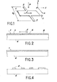
- the Hall effect is a known physical principle widely used for the measurement of magnetic fields, the essentials of which will be recalled with reference to FIG. 1.
- a semiconductor body 1 is placed in an induction B and traversed by a current 1 I and B perpendicular).
- Hall voltage is called the voltage VH which appears between the sides 2 and 3 parallel to the current 1 which flows in the semiconductor 1 when the latter is subjected to the perpendicular magnetic induction B. It is due to the deflection by magnetic induction B of the electrons in motion in the semiconductor 1.
- n is the number of conduction electrons per cubic centimeter
- t the thickness of the material
- e the charge of the electron
- Another criterion that has become important today when developing a new sensor manufacturing technology is its ability to allow collective and therefore economical manufacturing of large quantities of small sensors.
- the oldest and most used technology today to make hall effect detectors consists of taking ingots of single crystals of InSb or In As, cutting them into slices, sticking these slices on a substrate, thinning these slices by polishing , then to engrave the material to have the desired shape of the sensors.
- condition 1 is very well satisfied since an almost perfect single crystal can be used; condition 4 can be partially satisfied; on the other hand, conditions 2 and 3 are very poorly assured, because it is only at the cost of great precautions that we arrive at thicknesses of the order of 10 ⁇ m, which remains despite everything a high value.
- this high thickness limits the fineness of the etchings and therefore the sensor dimensions that can be produced (several tens of microns) while many applications require sensors of the order of a micron.
- condition 1 is very poorly satisfied.
- the material obtained by vacuum deposition is in fact polycrystalline, that is to say made up of a multitude of very small crystals which considerably limit the mobility of the electrons. Mobility is generally less than 1000 cm 2 / Vs for InSb. It can exceptionally reach 10,000 cm 2 / Vs under deposition conditions which are very difficult to control and this in any case with very poor reproducibility.
- This author has imagined a recrystallization method that can be called "hot wire method”. A mobility close to that of the single crystal could indeed be obtained.
- This method shown diagrammatically in FIG. 2, consists in placing in the vicinity of the thin layer 1 deposited on the substrate 4 a taut resistive wire 5, in melting the layer 1 over a narrow width 6 (-1 mm) by passing a electric current in the wire 5, and to move this molten zone 6 by moving the wire 5 in front of the substrate 1. The molten zone 6 thus separates the polycrystalline part 7 from the recrystallized part 8 of the semiconductor 1.
- heating wire method Another disadvantage of the heating wire method is that it can lead to very high thermal stresses in the substrate. In certain cases (detector on garnet for bubble memories for example) this is sufficient to break the substrate and to prohibit any use.
- the present invention specifically relates to a method of manufacturing Hall effect sensors in thin layers, which allows, while being a recrystallization method after deposition, to solve in a particularly simple and effective manner all the problems previously recalled from the prior art.
- the vacuum deposition of the semiconductor layer on a substrate can be carried out by vacuum evaporation.
- cathode sputtering can advantageously be used so as to obtain a homogeneous material and therefore suitable for precise subsequent microlithography operations.
- the shape chosen for the active parts of the sensors which is produced by chemical etching or by ion bombardment, consists in placing in parallel or in series elongated narrow strips , typically less than 20 wide ! lm.
- the fact of thus drawing a sensor whose active zones consist of narrow elements brings two fundamental advantages: firstly it makes it possible to have a heating current in the localized heating resistors of reasonable value, that is to say say relatively weak; then it makes it possible to avoid during recrystallization of the narrow strips of semiconductor a lack of uniformity of thickness because, over such a short width, the liquid semiconductor does not have the possibility of forming waves which would then be frozen during solidification.
- Another important advantage of the process according to the invention stems from the fact that the conductive metal layer which covers the areas to be recrystallized is well located and makes it possible to obtain heating of this latter area and only of this area very precisely.
- the various stages of manufacture of the method which is the subject of the invention allow without difficulty the simultaneous production of a large number of microscopic Hall effect sensors, from the same layer of semiconductors deposited on a substrate. This is a non-negligible advantage of the present process compared to the previously used mobile heating wire method.
- the heating resistors are etched slightly off center with respect to the longitudinal axis of the part of the narrow strip of semiconductor used in the sensor.
- the two solidification fronts which are symmetrical with respect to the resistance, and which symmetrically approach one of the other during cooling, come to meet along a line slightly offset by a few micrometers, for example relative to the center of the future active band of the Hall effect sensor.
- a zone fusion entrainment of the impurities possibly contained in the semiconductor is produced towards one of the lateral edges of the active strip, which eliminates the harmful effect of these impurities by allowing a significant improvement in the ratio 1 / ne in which n is the number of conduction electrons per cm 3 of the semiconductor and e the elementary charge of each electron.
- n is the number of conduction electrons per cm 3 of the semiconductor and e the elementary charge of each electron.
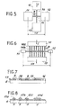
- Figure 3 there is shown the first step of the manufacturing process object of the invention which comprises depositing on a substrate 4, for example glass or ceramic, a semiconductor layer 1 of indium antimonide InSb.
- a substrate 4 for example glass or ceramic
- This deposition can be done by any known means, such as vacuum evaporation or preferably sputtering which gives a much more homogeneous material and therefore facilitates subsequent precise microlithography operations.
- Step 4 we have shown the following step which is a delimitation by cutting into a number of strips such as 9 of the previous semiconductor layer 1 in order to obtain active elements in the form of narrow strips, preferably of width less than 20 p, m.
- This cutting is also obtained by any known means such as chemical etching using a mask or ion bombardment making it possible to remove the semiconductor material with great precision at the desired locations.
- the senor it is preferable to draw the sensor in such a way that the active parts which are involved in the generation of the Hall voltage are made up of a certain number of bands or narrow elements placed in parallel or in series as is the case. shows in Figures 5 and 6 which give two possible examples of implementation.
- the sensor shown comprises four contact zones 10, 11, 12 and 13 which have not undergone recrystallization and two active strips 14 and 15 at right angles which are intended to undergo recrystallization in order to have mobility of the high negative charges.
- the electrodes 10 and 13 are used for the circulation of the bias current I in the conductive strip 14 and the electrodes 11 and 12 are used for sampling the Hall Vh voltage.
- the next step (FIG. 7) consists in depositing an insulating layer of silica SiO z on the structure obtained in FIG. 4.
- This layer 16 has a thickness of the order of 1 ! lm for example.
- the subsequent step of the process which is the subject of the invention consists in covering the silica layer 16 with a conductive and resistive metallic layer. 17 with a thickness of the order of 100 p, m (1000 A). This layer 17 most often consists of either a nickel-chromium NiCr alloy or tungsten W.
- this metallic layer After the deposition of this metallic layer, it is etched so as to constitute a certain number of heating resistors 17a, 17b, 17c and 17d visible in FIG. 8, each of which is located in line with the strips 9 of semiconductor material intended to be recrystallized .
- These different heating resistors are cut using a mask which can in particular be the same as that which was used for the etching of the semiconductor strips 9.
- the current of the heating resistors 17 causes the melting of the indium antimonide InSb, the current injection being able to be done for example using spikes.
- this structure makes it possible to use a relatively low heating current therefore of reasonable value and thus avoids the lack of uniformity in thickness of the layer of indium antimonide because, over such a short width, the phase liquid does not have the possibility of forming waves which could then be frozen during solidification.
- the heating resistors 17 are first removed and then the layer of SiO z on the non-recrystallized zones.
- the heating resistors 17 are removed using a solution containing S0 4 H z at 25% and at 60 ° C. in a commercial solution “CHROME-ETCH” well known.
- Silica Si0 2 is attacked chemically, for example using hydrofluoric acid.
- the last operation intervenes which consists in etching a conductive layer (for example an alloy of chromium and gold CrAu or copper Cu) in the holes of silica to obtain the contacts necessary for the electrical exploitation of the sensor .
- a conductive layer for example an alloy of chromium and gold CrAu or copper Cu
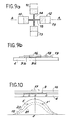
- the conductive layer of copper or chromium-gold alloy is shown at 18; the semiconductor layer InSb comprises parts 9a which have been recrystallized during the previous melting operations using local heating resistors 17 and parts 9b which are not recrystallized.
- the conductive layer 18 allows the connection of the connections 19 connecting the sensor to the outside.
- the heating resistors 17 are slightly displaced by a few micrometers relative to the axis of the active part a, b, of the semiconductor conductive strips 9 so that during solidification from the molten zone 9, the projections of the solidification fronts c, b, cause them to meet at a point from which the impurities which will have been displaced by zone fusion will be concentrated; point d is offset from the center of the active band a, b, actually used for the Hall effect.
- the cooling curves 19, 20 and 21 are shown showing the temperatures in the molten zone 9 as a function of the distance from the axis of the resistor 17.
- the curve 19 shows the maximum temperature obtained at the time of the merger; the curve 21 corresponds to the case where this maximum temperature is the melting temperature, that is to say at the time when the solidification fronts c and b meet.
- curve 20 illustrates the case of an intermediate temperature at the center of the molten zone and the arrows F and F 'drawn make it possible to know, for this cooling temperature and at this time, the position of the solidification fronts.
- the process which is the subject of the invention which has just been described has the great advantage of requiring no mechanical operation and of being able to be carried out in the open air with the conventional equipment of microelectronics. It allows the production of Hall effect sensors with good efficiency thanks to a high mobility of negative charges where it is useful and having dimensions and thicknesses as small as desired with the advantages of collective manufacturing on any what a substrate even fragile. It only requires a very low total energy supply during the recrystallization step.
Landscapes
- Engineering & Computer Science (AREA)
- Manufacturing & Machinery (AREA)
- Hall/Mr Elements (AREA)
Claims (3)
Applications Claiming Priority (2)
| Application Number | Priority Date | Filing Date | Title |
|---|---|---|---|
| FR8410363A FR2566964B1 (fr) | 1984-06-29 | 1984-06-29 | Procede de fabrication de capteurs a effet hall en couches minces |
| FR8410363 | 1984-06-29 |
Publications (2)
| Publication Number | Publication Date |
|---|---|
| EP0168312A1 EP0168312A1 (de) | 1986-01-15 |
| EP0168312B1 true EP0168312B1 (de) | 1988-12-28 |
Family
ID=9305634
Family Applications (1)
| Application Number | Title | Priority Date | Filing Date |
|---|---|---|---|
| EP85401285A Expired EP0168312B1 (de) | 1984-06-29 | 1985-06-25 | Verfahren zum Herstellen von Halleffektsensoren in Dünnschichten |
Country Status (5)
| Country | Link |
|---|---|
| US (1) | US4667391A (de) |
| EP (1) | EP0168312B1 (de) |
| JP (1) | JPS6119182A (de) |
| DE (1) | DE3567129D1 (de) |
| FR (1) | FR2566964B1 (de) |
Cited By (1)
| Publication number | Priority date | Publication date | Assignee | Title |
|---|---|---|---|---|
| WO2016131565A1 (de) * | 2015-02-18 | 2016-08-25 | Robert Bosch Gmbh | Verfahren zur herstellung eines hallsensors |
Families Citing this family (10)
| Publication number | Priority date | Publication date | Assignee | Title |
|---|---|---|---|---|
| JP2522214B2 (ja) * | 1989-10-05 | 1996-08-07 | 日本電装株式会社 | 半導体装置およびその製造方法 |
| US5054467A (en) * | 1990-12-10 | 1991-10-08 | Videtto Jr Donald W | Solar hot dog cooker |
| US6002252A (en) * | 1991-05-22 | 1999-12-14 | Wolff Controls Corporation | Compact sensing apparatus having transducer and signal conditioner with a plurality of mounting pins |
| US5543988A (en) * | 1993-04-30 | 1996-08-06 | International Business Machines Corporation | Hall sensor with high spatial resolution in two directions concurrently |
| JP3227985B2 (ja) * | 1994-04-06 | 2001-11-12 | 富士電機株式会社 | 磁気センサ |
| US6180419B1 (en) * | 1996-09-19 | 2001-01-30 | National Science Council | Method of manufacturing magnetic field transducer with improved sensitivity by plating a magnetic film on the back of the substrate |
| US9007060B2 (en) | 2011-07-21 | 2015-04-14 | Infineon Technologies Ag | Electronic device with ring-connected hall effect regions |
| US8988072B2 (en) | 2011-07-21 | 2015-03-24 | Infineon Technologies Ag | Vertical hall sensor with high electrical symmetry |
| US9312472B2 (en) | 2012-02-20 | 2016-04-12 | Infineon Technologies Ag | Vertical hall device with electrical 180 degree symmetry |
| US8876413B2 (en) * | 2013-03-14 | 2014-11-04 | Avago Technologies General Ip (Singapore) Pte. Ltd. | Method and system for providing electromagnetic interference (EMI) shielding in an optical communications module |
Family Cites Families (10)
| Publication number | Priority date | Publication date | Assignee | Title |
|---|---|---|---|---|
| JPS529515B2 (de) * | 1972-11-08 | 1977-03-16 | ||
| JPS5190288A (en) * | 1975-02-05 | 1976-08-07 | Hakumakukanjisoshi | |
| JPS5426369U (de) * | 1977-07-25 | 1979-02-21 | ||
| JPS55123185A (en) * | 1979-03-16 | 1980-09-22 | Pioneer Electronic Corp | Manufacture of semiconductor hall element |
| US4429321A (en) * | 1980-10-23 | 1984-01-31 | Canon Kabushiki Kaisha | Liquid jet recording device |
| DE3279842D1 (en) * | 1981-04-16 | 1989-08-31 | Massachusetts Inst Technology | Lateral epitaxial growth by seeded solidification |
| JPS5861622A (ja) * | 1981-10-09 | 1983-04-12 | Hitachi Ltd | 単結晶薄膜の製造方法 |
| JPS598691A (ja) * | 1982-07-06 | 1984-01-17 | Alps Electric Co Ltd | マイクロ・ゾ−ンメルト法 |
| JPS59128292A (ja) * | 1983-01-05 | 1984-07-24 | Seiko Instr & Electronics Ltd | 薄膜の結晶化方法 |
| US4576676A (en) * | 1983-05-24 | 1986-03-18 | Massachusetts Institute Of Technology | Thick crystalline films on foreign substrates |
-
1984
- 1984-06-29 FR FR8410363A patent/FR2566964B1/fr not_active Expired
-
1985
- 1985-06-19 JP JP60132124A patent/JPS6119182A/ja active Pending
- 1985-06-19 US US06/746,534 patent/US4667391A/en not_active Expired - Fee Related
- 1985-06-25 EP EP85401285A patent/EP0168312B1/de not_active Expired
- 1985-06-25 DE DE8585401285T patent/DE3567129D1/de not_active Expired
Cited By (1)
| Publication number | Priority date | Publication date | Assignee | Title |
|---|---|---|---|---|
| WO2016131565A1 (de) * | 2015-02-18 | 2016-08-25 | Robert Bosch Gmbh | Verfahren zur herstellung eines hallsensors |
Also Published As
| Publication number | Publication date |
|---|---|
| EP0168312A1 (de) | 1986-01-15 |
| FR2566964A1 (fr) | 1986-01-03 |
| FR2566964B1 (fr) | 1986-11-14 |
| US4667391A (en) | 1987-05-26 |
| DE3567129D1 (en) | 1989-02-02 |
| JPS6119182A (ja) | 1986-01-28 |
Similar Documents
| Publication | Publication Date | Title |
|---|---|---|
| EP0168312B1 (de) | Verfahren zum Herstellen von Halleffektsensoren in Dünnschichten | |
| EP0350351B1 (de) | Fotodiode und Fotodiodenmatrix aus II-VI-Halbleitermaterial und Herstellungsverfahren dafür | |
| JP3112680B2 (ja) | 半導体膜ボロメータ熱性赤外検出器 | |
| EP0596456B1 (de) | Methode zur Herstellung eines integrierten kapazitiven Transduktors | |
| CA1071743A (en) | Pyroelectric-field effect electromagnetic radiation detector | |
| EP0152325B1 (de) | Herstellungsverfahren einer Wicklung für Aufnahmemagnetkopf und Wicklung hergestellt nach diesem Verfahren | |
| FR2463978A1 (fr) | Cellule solaire integree avec une diode de derivation et son procede de fabrication | |
| CH691559A5 (fr) | Micro-contacteur magnétique et son procédé de fabrication. | |
| EP3577683B1 (de) | Struktur für funkfrequenzanwendungen | |
| EP0096611B1 (de) | Hochfrequenter piezoelektrischer Schwinger und Herstellungsverfahren | |
| EP0199638B1 (de) | Verfahren zur Herstellung auf einem Isoliersubstrat eines gerichteten einkristallinen Siliziumfilms mit lokalisierten Fehlern | |
| EP1402585B1 (de) | Verfahren zur massenherstellung einer grossen anzahl von magnetischen sensoren | |
| FR3062398A1 (fr) | Procede de fabrication d'un substrat pour la croissance d'un film bidimensionnel de structure cristalline hexagonale | |
| EP0229574B1 (de) | Photovoltaischer HgCdTe-Heteroübergang-Detektor und Verfahren zu seiner Herstellung | |
| EP0339069B1 (de) | Verfahren zur detektion des endes eines schleifvorganges für einen dünnschichtmagnetkopf | |
| EP3633336A1 (de) | Pyroelektrische detektionsvorrichtung mit starrer membran | |
| FR2910456A1 (fr) | Procede de realisation de microfils et/ou de nanofils | |
| EP0874379B1 (de) | Magnetischer Mikroschalter und Herstellungsverfahren | |
| FR2580672A1 (fr) | Procede de fabrication sur un support isolant d'un film de silicium monocristallin oriente et a defauts localises | |
| FR2781931A1 (fr) | Thermopiles a thermojonctions du type distribuees, fluxmetres thermiques radiatif et conductif mettant en oeuvre ces thermopiles, ainsi que leurs procedes de fabrication | |
| FR2604822A1 (fr) | Procede de formation d'une resistance sur un substrat | |
| FR2663157A1 (fr) | Procede d'autoalignement des contacts metalliques sur un dispositif semiconducteur et semiconducteur autoaligne. | |
| JP2742287B2 (ja) | 赤外線センサおよびその製造方法 | |
| CH620545A5 (en) | Method of manufacturing electrical resistors from a metal foil or film, application to obtaining thermoelectrical probes or strain gauges | |
| FR3119888A1 (fr) | Dispositif pyroelectrique comprenant un substrat a couche superficielle pyroelectrique et procede de realisation |
Legal Events
| Date | Code | Title | Description |
|---|---|---|---|
| PUAI | Public reference made under article 153(3) epc to a published international application that has entered the european phase |
Free format text: ORIGINAL CODE: 0009012 |
|
| AK | Designated contracting states |
Designated state(s): DE GB IT NL |
|
| 17P | Request for examination filed |
Effective date: 19860623 |
|
| RAP1 | Party data changed (applicant data changed or rights of an application transferred) |
Owner name: COMMISSARIAT A L'ENERGIE ATOMIQUE |
|
| 17Q | First examination report despatched |
Effective date: 19880105 |
|
| GRAA | (expected) grant |
Free format text: ORIGINAL CODE: 0009210 |
|
| AK | Designated contracting states |
Kind code of ref document: B1 Designated state(s): DE GB IT NL |
|
| ITF | It: translation for a ep patent filed | ||
| REF | Corresponds to: |
Ref document number: 3567129 Country of ref document: DE Date of ref document: 19890202 |
|
| GBT | Gb: translation of ep patent filed (gb section 77(6)(a)/1977) | ||
| PGFP | Annual fee paid to national office [announced via postgrant information from national office to epo] |
Ref country code: DE Payment date: 19890526 Year of fee payment: 5 |
|
| ITTA | It: last paid annual fee | ||
| PGFP | Annual fee paid to national office [announced via postgrant information from national office to epo] |
Ref country code: NL Payment date: 19890630 Year of fee payment: 5 Ref country code: GB Payment date: 19890630 Year of fee payment: 5 |
|
| PLBE | No opposition filed within time limit |
Free format text: ORIGINAL CODE: 0009261 |
|
| STAA | Information on the status of an ep patent application or granted ep patent |
Free format text: STATUS: NO OPPOSITION FILED WITHIN TIME LIMIT |
|
| 26N | No opposition filed | ||
| PG25 | Lapsed in a contracting state [announced via postgrant information from national office to epo] |
Ref country code: GB Effective date: 19900625 |
|
| PG25 | Lapsed in a contracting state [announced via postgrant information from national office to epo] |
Ref country code: NL Effective date: 19910101 |
|
| NLV4 | Nl: lapsed or anulled due to non-payment of the annual fee | ||
| GBPC | Gb: european patent ceased through non-payment of renewal fee | ||
| PG25 | Lapsed in a contracting state [announced via postgrant information from national office to epo] |
Ref country code: DE Effective date: 19910301 |