EP3577683B1 - Struktur für funkfrequenzanwendungen - Google Patents
Struktur für funkfrequenzanwendungen Download PDFInfo
- Publication number
- EP3577683B1 EP3577683B1 EP18705431.7A EP18705431A EP3577683B1 EP 3577683 B1 EP3577683 B1 EP 3577683B1 EP 18705431 A EP18705431 A EP 18705431A EP 3577683 B1 EP3577683 B1 EP 3577683B1
- Authority
- EP
- European Patent Office
- Prior art keywords
- layer
- dielectric layer
- conductive
- trapping
- radio frequency
- Prior art date
- Legal status (The legal status is an assumption and is not a legal conclusion. Google has not performed a legal analysis and makes no representation as to the accuracy of the status listed.)
- Active
Links
Images



Classifications
-
- H—ELECTRICITY
- H01—ELECTRIC ELEMENTS
- H01Q—ANTENNAS, i.e. RADIO AERIALS
- H01Q23/00—Antennas with active circuits or circuit elements integrated within them or attached to them
-
- H—ELECTRICITY
- H10—SEMICONDUCTOR DEVICES; ELECTRIC SOLID-STATE DEVICES NOT OTHERWISE PROVIDED FOR
- H10D—INORGANIC ELECTRIC SEMICONDUCTOR DEVICES
- H10D30/00—Field-effect transistors [FET]
- H10D30/01—Manufacture or treatment
- H10D30/021—Manufacture or treatment of FETs having insulated gates [IGFET]
- H10D30/031—Manufacture or treatment of FETs having insulated gates [IGFET] of thin-film transistors [TFT]
- H10D30/0321—Manufacture or treatment of FETs having insulated gates [IGFET] of thin-film transistors [TFT] comprising silicon, e.g. amorphous silicon or polysilicon
- H10D30/0323—Manufacture or treatment of FETs having insulated gates [IGFET] of thin-film transistors [TFT] comprising silicon, e.g. amorphous silicon or polysilicon comprising monocrystalline silicon
-
- H—ELECTRICITY
- H01—ELECTRIC ELEMENTS
- H01Q—ANTENNAS, i.e. RADIO AERIALS
- H01Q1/00—Details of, or arrangements associated with, antennas
- H01Q1/12—Supports; Mounting means
- H01Q1/22—Supports; Mounting means by structural association with other equipment or articles
- H01Q1/2283—Supports; Mounting means by structural association with other equipment or articles mounted in or on the surface of a semiconductor substrate as a chip-type antenna or integrated with other components into an IC package
-
- H—ELECTRICITY
- H10—SEMICONDUCTOR DEVICES; ELECTRIC SOLID-STATE DEVICES NOT OTHERWISE PROVIDED FOR
- H10D—INORGANIC ELECTRIC SEMICONDUCTOR DEVICES
- H10D30/00—Field-effect transistors [FET]
- H10D30/60—Insulated-gate field-effect transistors [IGFET]
- H10D30/67—Thin-film transistors [TFT]
- H10D30/6704—Thin-film transistors [TFT] having supplementary regions or layers in the thin films or in the insulated bulk substrates for controlling properties of the device
- H10D30/6708—Thin-film transistors [TFT] having supplementary regions or layers in the thin films or in the insulated bulk substrates for controlling properties of the device for preventing the kink effect or the snapback effect, e.g. discharging the minority carriers of the channel region for preventing bipolar effect
- H10D30/6711—Thin-film transistors [TFT] having supplementary regions or layers in the thin films or in the insulated bulk substrates for controlling properties of the device for preventing the kink effect or the snapback effect, e.g. discharging the minority carriers of the channel region for preventing bipolar effect by using electrodes contacting the supplementary regions or layers
-
- H—ELECTRICITY
- H10—SEMICONDUCTOR DEVICES; ELECTRIC SOLID-STATE DEVICES NOT OTHERWISE PROVIDED FOR
- H10D—INORGANIC ELECTRIC SEMICONDUCTOR DEVICES
- H10D30/00—Field-effect transistors [FET]
- H10D30/60—Insulated-gate field-effect transistors [IGFET]
- H10D30/67—Thin-film transistors [TFT]
- H10D30/6758—Thin-film transistors [TFT] characterised by the insulating substrates
-
- H—ELECTRICITY
- H10—SEMICONDUCTOR DEVICES; ELECTRIC SOLID-STATE DEVICES NOT OTHERWISE PROVIDED FOR
- H10P—GENERIC PROCESSES OR APPARATUS FOR THE MANUFACTURE OR TREATMENT OF DEVICES COVERED BY CLASS H10
- H10P90/00—Preparation of wafers not covered by a single main group of this subclass, e.g. wafer reinforcement
- H10P90/19—Preparing inhomogeneous wafers
- H10P90/1904—Preparing vertically inhomogeneous wafers
- H10P90/1906—Preparing SOI wafers
- H10P90/1914—Preparing SOI wafers using bonding
-
- H—ELECTRICITY
- H10—SEMICONDUCTOR DEVICES; ELECTRIC SOLID-STATE DEVICES NOT OTHERWISE PROVIDED FOR
- H10W—GENERIC PACKAGES, INTERCONNECTIONS, CONNECTORS OR OTHER CONSTRUCTIONAL DETAILS OF DEVICES COVERED BY CLASS H10
- H10W10/00—Isolation regions in semiconductor bodies between components of integrated devices
- H10W10/10—Isolation regions comprising dielectric materials
- H10W10/181—Semiconductor-on-insulator [SOI] isolation regions, e.g. buried oxide regions of SOI wafers
-
- H—ELECTRICITY
- H10—SEMICONDUCTOR DEVICES; ELECTRIC SOLID-STATE DEVICES NOT OTHERWISE PROVIDED FOR
- H10W—GENERIC PACKAGES, INTERCONNECTIONS, CONNECTORS OR OTHER CONSTRUCTIONAL DETAILS OF DEVICES COVERED BY CLASS H10
- H10W20/00—Interconnections in chips, wafers or substrates
- H10W20/01—Manufacture or treatment
- H10W20/031—Manufacture or treatment of conductive parts of the interconnections
- H10W20/032—Manufacture or treatment of conductive parts of the interconnections of conductive barrier, adhesion or liner layers
- H10W20/033—Manufacture or treatment of conductive parts of the interconnections of conductive barrier, adhesion or liner layers in openings in dielectrics
- H10W20/035—Manufacture or treatment of conductive parts of the interconnections of conductive barrier, adhesion or liner layers in openings in dielectrics combinations of barrier, adhesion or liner layers, e.g. multi-layered barrier layers
Definitions
- the present invention relates to structures for radio frequency applications. It relates in particular to a silicon-on-insulator type structure comprising a trapping layer and a buried electrode.
- Integrated devices are usually developed on substrates in the form of wafers, which mainly serve as a support for their manufacture.
- the increase in the degree of integration and the performance expected from these devices leads to an increasingly important coupling between their performance and the characteristics of the substrate on which they are formed.
- This is particularly the case of radiofrequency (RF) devices, processing signals whose frequency is between about 3kHz and 300GHz, which find their application in particular in the field of telecommunications (cellular telephony, Wi-Fi, Bluetooth, etc.). .
- RF radiofrequency
- the electromagnetic fields originating from the high-frequency signals propagating in the devices, penetrate into the depth of the substrate and interact with any charge carriers therein. This leads to problems of non-linear distortion of the signal (harmonics), unnecessary consumption of part of the signal energy by insertion loss and possible influences between components.
- high resistivity silicon-based substrates comprising a support substrate, a trapping layer placed on the support substrate, a dielectric layer placed on the trapping layer, and a layer of semiconductor disposed on the dielectric layer.
- the support substrate usually has a resistivity greater than 1 kOhm.cm.
- the trapping layer may comprise undoped polycrystalline silicon.
- the document US2016/336991 proposes a solution for improving the performance of RF devices on SOI, comprising in particular a contact layer electrically connected to the support substrate.
- An object of the invention is in particular to propose a structure for radiofrequency application allowing the production of RF devices with improved performance.
- the present invention relates to a structure for radio frequency application according to claim 1.
- the figures are schematic representations which, for the purpose of readability, are not to scale.
- the thicknesses of the layers along the z axis are not to scale with respect to the lateral dimensions along the x and y axes.
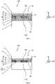
- the invention relates to a structure 100 for radio frequency application comprising a support substrate 1 with high resistivity.
- high resistivity is meant a resistivity greater than 1000 ohm.cm; it is advantageously between 4 and 10 kohm.cm.
- the support substrate 1 can be made of materials usually used in the microelectronics, optics, optoelectronics, photovoltaics industry.
- the support substrate 1 can comprise at least one material selected from the following group: silicon, silicon germanium, silicon carbide, etc.
- the front face la of the support substrate 1 defines a main plane (x,y) as illustrated in FIG.
- the support substrate 1 has the shape of a circular plate, with a diameter of 150, 200, 300, or even 450 mm.
- the structure 100 also comprises a charge trapping layer 2 arranged on the front face 1a of the support substrate 1.
- a charge trapping layer 2 arranged on the front face 1a of the support substrate 1.
- the trapping layer 2 can be either directly in contact with the front face 1a of the support substrate 1, either secured thereto via one or more intermediate layers.
- the term “disposed” used hereafter should be interpreted in a similar manner.
- the trapping layer 2 comprises a material of polycrystalline silicon type, the defect density of which is favorable to the trapping of free electric charges, able to develop in the support substrate 1.
- the trapping layer 2 could also include other types of materials capable of ensuring the trapping function and compatible with the structure 100 and its use.
- the trapping layer 2 has a thickness comprised between a few tens of nanometers and a few microns, for example between 50 nm and 3 microns.
- the structure 100 further comprises a first dielectric layer 3 placed on the trapping layer 2.
- the first dielectric layer 3 will constitute, in certain embodiments according to the invention, the buried insulating layer of the structure 100, which will in particular insulate electrically the active layer 4 of the support substrate 1.
- the first dielectric layer 3 will comprise at least one of the materials from among: silicon dioxide, silicon nitride, aluminum oxide, etc. thickness can for example vary between 10 nm and 3 ⁇ m.
- the structure 100 also comprises an active layer 4 placed on the first dielectric layer 3.
- the active layer 4 corresponds to the layer in and/or on which RF components can be produced. It has a free face or face front 4a and a rear face 4b integral with the underlying layers.
- the active layer 4 may advantageously consist of semiconductor materials and/or piezoelectric materials.
- the active layer 4 comprises at least one of the materials from among: silicon, silicon carbide, silicon germanium, lithium niobate, lithium tantalate, quartz, aluminum nitride, etc.
- active layer 4 can have a thickness ranging from a few nanometers (for example 10 nm) to a few microns, or even a few tens of microns (for example 50 ⁇ m), depending on the components to be manufactured.
- the structure 100 according to the invention comprises at least one buried electrode 10 arranged above or in the trapping layer 2:
- FIG. la illustrates an embodiment in which the buried electrode 10 is located above the trapping layer 2; in particular, it is located just below the active layer 4.
- the buried electrode 10 comprises an electrically conductive layer 11 and a dielectric layer 13 (hereinafter called second dielectric layer 13).
- the buried electrode 10 is intended to be polarized by the application of a voltage to the conductive layer 11, and to generate an effect on the electric carriers of the active layer 4.
- the conductive layer 11 comprises a material chosen from monocrystalline silicon, polycrystalline silicon, amorphous silicon, etc. or other materials usually used for the manufacture of gate electrodes or resistors in microelectronics .
- the material forming the conductive layer 11 advantageously has a resistivity ranging from a few ohms.cm to a few thousand ohms.cm. It will preferably be chosen to be compatible with high temperature treatments, the structure 100 being likely to be subjected to such treatments for the manufacture of radio frequency components.
- the conductive layer 11 has a typical thickness comprised between 50 nm and 500 nm.
- the second dielectric layer 13 can comprise at least one of the materials from among: silicon dioxide, silicon nitride, aluminum oxide, etc. It advantageously has a thickness of between 5 nm and 100 nm. Nevertheless, its thickness may vary between 1 nm and 3 ⁇ m, depending on the embodiments of the invention.
- Conductive layer 11 has two faces 11a, 11b along the main plane (x,y): in the example of picture 1a , the first face 11a is in contact with the second dielectric layer 13 and the second face 11b is in contact with the first dielectric layer 3.
- the electrode 10 comprises a plurality of electrically insulating walls 14, extending between the first dielectric layer 3 and the second dielectric layer 13 ( figure 1b and 2b ). Said insulating walls 14 segment the conductive layer 11 into a plurality of conductive blocks 12, insulated from each other by said insulating walls 14.
- the conductive block 12 of the buried electrode 10 which is electrically insulated from the other layers of the structure 100, and in particular from the active layer 4 and from the support substrate 1.
- the conductive block 12 is advantageously located at least opposite the active region of a transistor which will be produced in the active layer 4: said transistor can then benefit from a bias at the level of the face rear 4b of active layer 4, in addition to its usual polarization by a gate electrode.
- a back bias (back bias" according to the Anglo-Saxon terminology) makes it possible to increase the breakdown voltage of the transistor and thus limits the number of transistors to be put in series to withstand the voltage applied to the terminals of the RF device (switch for example).
- the series resistance of the device can be reduced and its linearity is improved.
- electrode 10 is placed between active layer 4 and first dielectric layer 3, second dielectric layer 13 being in contact with active layer 4, along the plane main (x,y).
- the second dielectric layer 13 has a thickness of less than 400 nm, preferably of the order of 50-100 nm, so that the voltage applied to the conductive layer 11 of the buried electrode 10 can have an effect on the electric carriers of the active layer 4.
- the structure 100 presented in FIG. 1a can be produced by different methods. Some manufacturing variants are described below.
- Charge trapping layer 2 is first deposited on support substrate 1.
- a layer of polycrystalline silicon constituting trapping layer 2 may be deposited by a chemical vapor deposition technique or by liquid phase or else by epitaxy on a support substrate 1 made of silicon.
- the trapping layer 2 has a thickness comprised in the range stated previously, for example of the order of 2 microns.
- the bonding interface is located between the second dielectric layer 13 and the conductive layer 11.
- the second dielectric layer 13 has been formed on the donor substrate; by way of example, this layer consists of a layer of silicon oxide, thermally greened on the donor substrate.
- the first dielectric layer 3, then the conductive layer 11, are successively deposited on the trapping layer 2.
- the first dielectric layer 3 consists for example of a layer of thermally raw silicon oxide on the trapping layer 2 or deposited by chemical deposition; the conductive layer 11 consists of a layer of polycrystalline silicon, the resistivity of which may be between a few ohms.cm and a few kohms.cm.
- the conductive layer 11 comprises insulating walls 14, which define a plurality of conductive blocks 12.
- the formation of the conductive layer 11 then requires at least one step of lithography and etching to define the distribution in the plane (x,y) of the conductive blocks 12 and the insulating walls 14 and form them successively.
- the bonding interface is located between the conductive layer 11 and the first dielectric layer 3.
- the second dielectric layer 13 is formed on the donor substrate, then the conductive layer 11 is formed on second dielectric layer 13.
- first dielectric layer 3 is deposited on trapping layer 2 secured to support substrate 1.
- the bonding interface is located between the first dielectric layer 3 and the trapping layer 2.
- the second dielectric layer 13 is first formed on the donor substrate, then the layer conductive layer 11 is formed on the second dielectric layer 13, finally the first dielectric layer 3 is formed on the conductive layer 11.
- the bonding interface can be located in one of the intermediate layers, for example in the middle of the first dielectric layer 3.
- a first part of the first dielectric layer 3 is formed on the donor substrate (from which the active layer 4 originates); a second part of the first dielectric layer 3 is formed on the side of the support substrate 1, after the formation of the underlying layers.
- the donor and support substrates are assembled by molecular adhesion.
- the implementation of one or other of the previous layer transfer techniques then leads to the formation of the active layer 4.
- the electrode 10 is placed between the first dielectric layer 3 and the charge trapping layer 2, the second dielectric layer 13 being in contact with the trapping layer, along the main plane (x,y).
- the first face 11a of the conductive layer 11 is in contact with the first dielectric layer 3 and its second face 11b is in contact with second dielectric layer 13.
- the first dielectric layer 3 has a thickness of less than 400 nm, preferably less than 200 nm, so that the voltage applied to the conductive layer 11 of the buried electrode 10 can have an effect on the electric carriers of the layer. active 4.
- the second dielectric layer 13 can itself have a thickness of up to a few microns, if this is required for the application.
- the electrode 10 is arranged as before between the first dielectric layer 3 and the charge trapping layer 2 and it comprises conductive blocks 12 electrically insulated from each other by insulating walls 14; moreover, the buried electrode 10 is discontinuous in the main plane (x,y) and a plurality of charge trapping zones 22 extend between the first dielectric layer 3 and the charge trapping layer 2.
- the charge trapping zones trapping 22 are isolated from the conductive blocks 12 by the insulating walls 14.
- the trapping zones 22 may be formed by the same material as the trapping layer 2 or by a different material, having properties for trapping electric charges.
- the first dielectric layer 3 has a thickness of less than 400 nm, preferably less than 200 nm, so that the voltage applied to the conductive layer 11 of the buried electrode 10 can have an effect on the electrical carriers of the active layer 4.
- the layer transfer techniques detailed for the first embodiment also apply to this third embodiment.
- an assembly option consisting in placing the bonding interface in the first dielectric layer 3 will be implemented.
- a first part of the first dielectric layer 3 is formed on the donor substrate (from which the active layer 4 originates); a second part of the first dielectric layer 3 is formed on the side of the support substrate 1, after the formation of the underlying layers.
- the trapping layer 2 is first produced on the support substrate 1.
- the second dielectric layer 13 is then deposited (chemical deposition or thermal growth). A lithography and etching step makes it possible to eliminate the second dielectric layer 13 at the level of the future trapping zones 22.
- the donor and support substrates are then assembled by molecular adhesion.
- the implementation of one or the other of the previously stated layer transfer techniques then leads to the formation of the active layer 4.
- the electrode 10 is placed in the charge trapping layer 2.
- the second dielectric layer 13 is in contact with the front face 1a of the support substrate 1 along the main plane (x, y).
- the electrode 10 comprises a plurality of insulating walls 14 extending between the first 3 and the second 13 dielectric layer and defining a plurality of conductive blocks 12 of the conductive layer 11, insulated from each other by said insulating walls 14.
- Each conductive pad 12 is electrically insulated from at least one charge trapping zone 23 forming the trapping layer 2, by the insulating walls 14.
- the charge trapping zone 23 extends between the first dielectric layer 3 and the support substrate 1.
- the structure 100 can comprise a third dielectric layer 30, arranged between the trapping layer 2 (or the charge trapping zones 23) and the support substrate 1. It can comprise at at least one of the materials among: silicon dioxide, silicon nitride, aluminum oxide, etc. It is particularly advantageous in that it prevents or at least strongly limits the recrystallization of the trapping layer 2, when the latter is for example made of polycrystalline silicon) during the heat treatments at high temperatures likely to be applied. for the manufacture of the structure according to the invention.
- At least one conductive block 12 can be electrically connected to a contact pad 40 by a conductive via 41.
- the latter crosses a part of the structure 100 to go from the conductive pad 12 to said contact pad 40; in the example of figure 5a , the conductive via 41 in particular passes through the active layer 4 and the second dielectric layer 13.
- the contact pad 40 is arranged on a free face 4a of the active layer 4, electrically insulated therefrom.
- the contact pad 40 is formed by an electrically conductive material through which a voltage can be applied to the conductive pad 12 of the buried electrode 10.
- the conductive via 41 is formed, by techniques known to those skilled in the art , by making a trench whose walls are electrically insulated from the layers through which it passes and which is filled with a conductive material, for example doped polycrystalline silicon.
- a plurality of conductive vias 41 can be made to independently connect each conductive block 12 buried to a contact pad 40.
- Alignment marks will advantageously have been formed on the support substrate 1 (or on the donor substrate from which the active layer 4 originates) during the development of the conductive pads 12. These alignment marks are used during the manufacturing steps conductive vias 41, in order to form the vias plumb with the conductive blocks 12.
- Structure 100 may also comprise a device in and/or on active layer 4, comprising at least one transistor 50, one gate electrode 51 of which disposed on free face 4a of active layer 4 facing at least least one conductive block 12 of the buried electrode 10 ( figure 5b ).
- the alignment marks formed during the development of the conductive pads 12 of the buried electrode 10 are also used during the manufacturing steps of the electronic device on the active layer 4.
- the structure 100 according to the invention is particularly suitable for radiofrequency devices such as in particular antenna switches or adapters for cellular telephones.
- the integration of the buried electrode 10 in the structure 100 allows easier manufacture of devices comprising transistors with “back bias”.
- the use of a buried electrode 10 to bias the active region 52 of a transistor 50 via the rear face (“back bias”) makes it possible to increase the breakdown voltage of the transistor and thus to limit the number of transistors to be put in parallel in each device.
- back bias the presence of the charge trapping layer 2 in the structure 100 ensures the maintenance of a high resistivity of the support substrate 1.
- the structure 100 according to the invention thus makes it possible to achieve high performance in the field of high-frequency applications.
Landscapes
- Engineering & Computer Science (AREA)
- Microelectronics & Electronic Packaging (AREA)
- Thin Film Transistor (AREA)
- Semiconductor Integrated Circuits (AREA)
- Waveguides (AREA)
- Physical Vapour Deposition (AREA)
Claims (11)
- Struktur (100) für Hochfrequenzanwendung, umfassend:• ein Trägersubstrat (1) mit hohem spezifischem Widerstand, dessen Vorderseite (1a) eine Hauptebene definiert,• eine auf der Vorderseite (1a) des Trägersubstrats (1) angeordnete Ladungseinfangschicht (2),• eine auf der Einfangschicht (2) angeordnete erste dielektrische Schicht (3),• eine auf der ersten dielektrischen Schicht (3) angeordnete aktive Schicht (4),wobei die Struktur (100) dadurch gekennzeichnet ist, dass sie mindestens eine verdeckte Elektrode (10) umfasst, die über oder in der Einfangschicht (2) angeordnet ist, wobei die Elektrode (10) umfasst:• eine leitfähige Schicht (11) und eine zweite dielektrische Schicht (13), wobei die leitfähige Schicht (11) von der aktiven Schicht (4), von der Einfangschicht (2) und von dem Trägersubstrat (1) elektrisch isoliert ist und die leitfähige Schicht (11) zwei Seiten (11a, 11b) entlang der Hauptebene aufweist, wobei eine Seite in Kontakt mit der ersten dielektrischen Schicht (3) steht und eine andere Seite in Kontakt mit der zweiten dielektrischen Schicht (13) steht,• mehrere isolierende Wände (14), die sich zwischen der ersten (3) und der zweiten (13) dielektrischen Schicht erstrecken und die leitfähige Schicht (11) in mehrere leitfähige Pads (12) segmentieren, wobei die Pads (12) voneinander durch die isolierenden Wände (14) isoliert sind, wobei mindestens ein leitfähiges Pad (12) so konfiguriert ist, dass es einem in der aktiven Schicht (4) herzustellenden Transistor eine Rückwärtsvorspannung bereitstellt.
- Struktur (100) für Hochfrequenzanwendung nach dem vorhergehenden Anspruch, bei der die Elektrode (10) zwischen der aktiven Schicht (4) und der ersten dielektrischen Schicht (3) angeordnet ist, wobei die zweite dielektrische Schicht (13) entlang der Hauptebene mit der aktiven Schicht (4) in Kontakt steht.
- Struktur (100) für Hochfrequenzanwendung nach Anspruch 1, bei der die Elektrode (10) zwischen der ersten dielektrischen Schicht (3) und der Ladungseinfangschicht (2) angeordnet ist, wobei die zweite dielektrische Schicht (13) entlang der Hauptebene mit der Einfangschicht (2) in Kontakt steht.
- Struktur (100) für Hochfrequenzanwendung nach dem vorhergehenden Anspruch, bei der die Elektrode (10) in der Hauptebene diskontinuierlich ist und sich eine Vielzahl von Ladungseinfangzonen (22) zwischen der ersten dielektrischen Schicht (3) und der Ladungseinfangschicht (2) erstrecken, wobei die Einfangzonen (22) von den leitfähigen Pads (12) durch die isolierenden Wände (14) isoliert sind.
- Struktur (100) für Hochfrequenzanwendung nach Anspruch 1, bei der die Elektrode (10) in der Ladungseinfangschicht (2) angeordnet ist, wobei die zweite dielektrische Schicht (13) mit der Vorderseite (1a) des Trägersubstrats (1) entlang der Hauptebene in Kontakt steht und bei dem die Elektrode (10) mehrere isolierende Wände (14) umfasst, die sich zwischen der ersten (3) und der zweiten (13) dielektrischen Schicht erstrecken und mehrere leitfähige Pads (12) der leitfähigen Schicht (11) definieren, wobei jedes leitfähige Pad (12) durch die isolierenden Wände (14) von mindestens einer Einfangzone (23) isoliert ist, die die Einfangschicht (2) bildet.
- Struktur (100) für Hochfrequenzanwendung nach Anspruch 1, bei der mindestens ein leitfähiges Pad (12) elektrisch mit einer Kontaktanschlussfläche (40), die auf einer freien Seite (4a) der aktiven Schicht (4) angeordnet ist, durch eine leitfähige Durchkontaktierung (41) verbunden ist, die durch einen Teil der Struktur (100) hindurchgeht, um vom leitfähigen Pad (12) zur Kontaktanschlussfläche (40) zu verlaufen.
- Struktur (100) für Hochfrequenzanwendung nach dem vorhergehenden Anspruch, die ferner eine Vorrichtung in und/oder auf der aktiven Schicht (4) umfasst, die mindestens einen Transistor (50) umfasst, dessen eine Gate-Elektrode (51), die auf der freien Seite (4a) der aktiven Schicht (4) angeordnet ist, sich gegenüber mindestens einem leitfähigen Pad (12) der verdeckten Elektrode (10) befindet.
- Struktur (100) für Hochfrequenzanwendung nach einem der vorhergehenden Ansprüche, bei der die zweite dielektrische Schicht (13) eine Dicke zwischen 5 nm und 100 nm aufweist.
- Struktur (100) für Hochfrequenzanwendung nach einem der vorhergehenden Ansprüche, bei der die leitfähige Schicht (11) ein Material umfasst, das aus monokristallinem Silizium, polykristallinem Silizium, amorphem Silizium ausgewählt ist.
- Struktur (100) für Hochfrequenzanwendung nach einem der vorhergehenden Ansprüche, bei der die leitfähige Schicht (11) eine Dicke zwischen 50 nm und 500 nm aufweist.
- Struktur (100) für Hochfrequenzanwendung nach einem der vorhergehenden Ansprüche, bei der die leitfähige Schicht einen spezifischen Widerstand zwischen einigen Ohm·cm und einigen tausend Ohm·cm aufweist.
Applications Claiming Priority (2)
| Application Number | Priority Date | Filing Date | Title |
|---|---|---|---|
| FR1750870A FR3062517B1 (fr) | 2017-02-02 | 2017-02-02 | Structure pour application radiofrequence |
| PCT/FR2018/050196 WO2018142052A1 (fr) | 2017-02-02 | 2018-01-29 | Structure pour application radiofréquence |
Publications (2)
| Publication Number | Publication Date |
|---|---|
| EP3577683A1 EP3577683A1 (de) | 2019-12-11 |
| EP3577683B1 true EP3577683B1 (de) | 2022-09-21 |
Family
ID=58779151
Family Applications (1)
| Application Number | Title | Priority Date | Filing Date |
|---|---|---|---|
| EP18705431.7A Active EP3577683B1 (de) | 2017-02-02 | 2018-01-29 | Struktur für funkfrequenzanwendungen |
Country Status (9)
| Country | Link |
|---|---|
| US (3) | US11043756B2 (de) |
| EP (1) | EP3577683B1 (de) |
| JP (1) | JP7098851B2 (de) |
| KR (1) | KR102520751B1 (de) |
| CN (1) | CN110235238B (de) |
| FR (1) | FR3062517B1 (de) |
| SG (1) | SG11201906975PA (de) |
| TW (1) | TWI764978B (de) |
| WO (1) | WO2018142052A1 (de) |
Families Citing this family (9)
| Publication number | Priority date | Publication date | Assignee | Title |
|---|---|---|---|---|
| FR3062517B1 (fr) * | 2017-02-02 | 2019-03-15 | Soitec | Structure pour application radiofrequence |
| FR3086096B1 (fr) * | 2018-09-14 | 2021-08-27 | Soitec Silicon On Insulator | Procede de realisation d'un substrat avance pour une integration hybride |
| FR3091004B1 (fr) * | 2018-12-24 | 2020-12-04 | Soitec Silicon On Insulator | Structure de type semi-conducteur pour applications digitales et radiofréquences |
| FR3091010B1 (fr) * | 2018-12-24 | 2020-12-04 | Soitec Silicon On Insulator | Structure de type semi-conducteur pour applications digitales et radiofréquences, et procédé de fabrication d’une telle structure |
| US11271079B2 (en) * | 2020-01-15 | 2022-03-08 | Globalfoundries U.S. Inc. | Wafer with crystalline silicon and trap rich polysilicon layer |
| TWI761255B (zh) * | 2021-07-08 | 2022-04-11 | 環球晶圓股份有限公司 | 晶圓及晶圓的製造方法 |
| FR3136325B1 (fr) * | 2022-06-02 | 2025-10-03 | Soitec Silicon On Insulator | Dispositif a ondes elastiques de surface |
| JP7609154B2 (ja) | 2022-11-11 | 2025-01-07 | 信越半導体株式会社 | 高周波デバイス用基板およびその製造方法 |
| CN116207036A (zh) * | 2023-02-28 | 2023-06-02 | 上海华虹宏力半导体制造有限公司 | 射频开关的形成方法 |
Citations (1)
| Publication number | Priority date | Publication date | Assignee | Title |
|---|---|---|---|---|
| WO2016087728A1 (fr) * | 2014-12-04 | 2016-06-09 | Soitec | Structure pour applications radiofréquences |
Family Cites Families (43)
| Publication number | Priority date | Publication date | Assignee | Title |
|---|---|---|---|---|
| EP0159601A3 (de) * | 1984-04-10 | 1987-08-19 | Hartwig Wolfgang Prof.Dr. Thim | Logik-Schaltungsanordnung mit dazu angepasst ausgebildeten Feldeffekt-Transistoren |
| US5841623A (en) * | 1995-12-22 | 1998-11-24 | Lam Research Corporation | Chuck for substrate processing and method for depositing a film in a radio frequency biased plasma chemical depositing system |
| JPH1041512A (ja) * | 1996-07-23 | 1998-02-13 | Denso Corp | 半導体装置 |
| JP2000058844A (ja) | 1998-08-10 | 2000-02-25 | Denso Corp | 半導体装置及び半導体装置の製造方法 |
| JP2004207271A (ja) * | 2002-12-20 | 2004-07-22 | Nec Electronics Corp | Soi基板及び半導体集積回路装置 |
| US6956278B2 (en) * | 2003-06-30 | 2005-10-18 | Matrix Semiconductor, Inc. | Low-density, high-resistivity titanium nitride layer for use as a contact for low-leakage dielectric layers |
| JP4773697B2 (ja) * | 2004-06-30 | 2011-09-14 | ルネサスエレクトロニクス株式会社 | Soi基板およびその製造方法ならびに半導体装置 |
| US7709313B2 (en) * | 2005-07-19 | 2010-05-04 | International Business Machines Corporation | High performance capacitors in planar back gates CMOS |
| US20100027355A1 (en) * | 2007-07-31 | 2010-02-04 | Dao Thuy B | Planar double gate transistor storage cell |
| US7993752B2 (en) * | 2008-03-17 | 2011-08-09 | Nano PV Technologies, Inc. | Transparent conductive layer and method |
| JP2010114165A (ja) * | 2008-11-04 | 2010-05-20 | Nikon Corp | 半導体装置、積層半導体装置および積層半導体装置の製造方法 |
| JP4917085B2 (ja) * | 2008-12-15 | 2012-04-18 | 東京エレクトロン株式会社 | 半導体装置 |
| US8133774B2 (en) * | 2009-03-26 | 2012-03-13 | International Business Machines Corporation | SOI radio frequency switch with enhanced electrical isolation |
| US8742459B2 (en) * | 2009-05-14 | 2014-06-03 | Transphorm Inc. | High voltage III-nitride semiconductor devices |
| FR2954626B1 (fr) * | 2009-12-23 | 2013-12-06 | Commissariat Energie Atomique | Resonateur acoustique comprenant un electret, et procede de fabrication de ce resonateur, application aux filtres commutables a resonateurs couples |
| FR2967812B1 (fr) * | 2010-11-19 | 2016-06-10 | S O I Tec Silicon On Insulator Tech | Dispositif electronique pour applications radiofrequence ou de puissance et procede de fabrication d'un tel dispositif |
| US8536021B2 (en) | 2010-12-24 | 2013-09-17 | Io Semiconductor, Inc. | Trap rich layer formation techniques for semiconductor devices |
| EP3734645B1 (de) | 2010-12-24 | 2025-09-10 | Qualcomm Incorporated | Schicht mit hoher haftstellendichte für halbleiterbauelemente |
| US8481405B2 (en) * | 2010-12-24 | 2013-07-09 | Io Semiconductor, Inc. | Trap rich layer with through-silicon-vias in semiconductor devices |
| FR2973158B1 (fr) | 2011-03-22 | 2014-02-28 | Soitec Silicon On Insulator | Procédé de fabrication d'un substrat de type semi-conducteur sur isolant pour applications radiofréquences |
| US9525399B2 (en) * | 2011-10-31 | 2016-12-20 | Avago Technologies General Ip (Singapore) Pte. Ltd. | Planarized electrode for improved performance in bulk acoustic resonators |
| CN103199110B (zh) * | 2012-01-09 | 2015-10-14 | 上海华虹宏力半导体制造有限公司 | 一种nldmos器件及其制造方法 |
| KR102360695B1 (ko) * | 2014-01-23 | 2022-02-08 | 글로벌웨이퍼스 씨오., 엘티디. | 고 비저항 soi 웨이퍼 및 그 제조 방법 |
| US20150228714A1 (en) * | 2014-02-13 | 2015-08-13 | Rfaxis, Inc. | Isolation methods for leakage, loss and non-linearity mitigation in radio-frequency integrated circuits on high-resistivity silicon-on-insulator substrates |
| US9269591B2 (en) | 2014-03-24 | 2016-02-23 | Taiwan Semiconductor Manufacturing Co., Ltd. | Handle wafer for high resistivity trap-rich SOI |
| US9209198B2 (en) * | 2014-05-12 | 2015-12-08 | Macronix International Co., Ltd. | Memory cell and manufacturing method thereof |
| US9917571B2 (en) * | 2014-06-13 | 2018-03-13 | Georgia Tech Research Corporation | Resonant gyroscopes and methods of making and using the same |
| FR3024587B1 (fr) * | 2014-08-01 | 2018-01-26 | Soitec | Procede de fabrication d'une structure hautement resistive |
| JP6650463B2 (ja) * | 2014-11-18 | 2020-02-19 | グローバルウェーハズ カンパニー リミテッドGlobalWafers Co.,Ltd. | 電荷トラップ層を備えた高抵抗率の半導体・オン・インシュレーターウェハーの製造方法 |
| TWI732383B (zh) * | 2015-02-06 | 2021-07-01 | 日商半導體能源研究所股份有限公司 | 裝置及其製造方法以及電子裝置 |
| JP6344271B2 (ja) | 2015-03-06 | 2018-06-20 | 信越半導体株式会社 | 貼り合わせ半導体ウェーハ及び貼り合わせ半導体ウェーハの製造方法 |
| WO2016161029A1 (en) * | 2015-03-31 | 2016-10-06 | Skyworks Solutions, Inc. | Substrate bias for field-effect transistor devices |
| TW201724510A (zh) * | 2015-05-15 | 2017-07-01 | 西凱渥資訊處理科技公司 | 使用基板開口之射頻隔離 |
| JP6595804B2 (ja) * | 2015-05-27 | 2019-10-23 | ソニーセミコンダクタソリューションズ株式会社 | 固体撮像素子および撮像装置 |
| US9514987B1 (en) * | 2015-06-19 | 2016-12-06 | International Business Machines Corporation | Backside contact to final substrate |
| US20160379943A1 (en) * | 2015-06-25 | 2016-12-29 | Skyworks Solutions, Inc. | Method and apparatus for high performance passive-active circuit integration |
| US9711521B2 (en) * | 2015-08-31 | 2017-07-18 | Taiwan Semiconductor Manufacturing Co., Ltd. | Substrate fabrication method to improve RF (radio frequency) device performance |
| FR3042648B1 (fr) * | 2015-10-20 | 2018-09-07 | Soitec Silicon On Insulator | Dispositif a ondes acoustiques de surface et procede de fabrication associe |
| FR3052592B1 (fr) * | 2016-06-08 | 2018-05-18 | Soitec | Structure pour applications radiofrequences |
| FR3062238A1 (fr) * | 2017-01-26 | 2018-07-27 | Soitec | Support pour une structure semi-conductrice |
| FR3062517B1 (fr) * | 2017-02-02 | 2019-03-15 | Soitec | Structure pour application radiofrequence |
| KR102722507B1 (ko) * | 2017-12-07 | 2024-10-29 | 인피니언 테크놀로지스 아게 | 음향적으로 결합된 공진기 노치 및 대역 통과 필터 |
| DE102018215018A1 (de) * | 2018-09-04 | 2020-03-05 | Infineon Technologies Ag | Feuchtigkeitssensor |
-
2017
- 2017-02-02 FR FR1750870A patent/FR3062517B1/fr active Active
-
2018
- 2018-01-29 WO PCT/FR2018/050196 patent/WO2018142052A1/fr not_active Ceased
- 2018-01-29 US US16/480,249 patent/US11043756B2/en active Active
- 2018-01-29 SG SG11201906975PA patent/SG11201906975PA/en unknown
- 2018-01-29 JP JP2019538653A patent/JP7098851B2/ja active Active
- 2018-01-29 EP EP18705431.7A patent/EP3577683B1/de active Active
- 2018-01-29 KR KR1020197024060A patent/KR102520751B1/ko active Active
- 2018-01-29 CN CN201880009739.5A patent/CN110235238B/zh active Active
- 2018-01-29 TW TW107103106A patent/TWI764978B/zh active
-
2021
- 2021-05-25 US US17/330,237 patent/US11502428B2/en active Active
-
2022
- 2022-08-01 US US17/816,599 patent/US12418120B2/en active Active
Patent Citations (1)
| Publication number | Priority date | Publication date | Assignee | Title |
|---|---|---|---|---|
| WO2016087728A1 (fr) * | 2014-12-04 | 2016-06-09 | Soitec | Structure pour applications radiofréquences |
Also Published As
| Publication number | Publication date |
|---|---|
| JP2020509576A (ja) | 2020-03-26 |
| CN110235238B (zh) | 2023-08-29 |
| WO2018142052A1 (fr) | 2018-08-09 |
| JP7098851B2 (ja) | 2022-07-12 |
| KR102520751B1 (ko) | 2023-04-12 |
| CN110235238A (zh) | 2019-09-13 |
| US20210280990A1 (en) | 2021-09-09 |
| US20190372243A1 (en) | 2019-12-05 |
| FR3062517A1 (fr) | 2018-08-03 |
| US20220368036A1 (en) | 2022-11-17 |
| TWI764978B (zh) | 2022-05-21 |
| TW201830660A (zh) | 2018-08-16 |
| US11043756B2 (en) | 2021-06-22 |
| SG11201906975PA (en) | 2019-08-27 |
| KR20190112738A (ko) | 2019-10-07 |
| FR3062517B1 (fr) | 2019-03-15 |
| US11502428B2 (en) | 2022-11-15 |
| EP3577683A1 (de) | 2019-12-11 |
| US12418120B2 (en) | 2025-09-16 |
Similar Documents
| Publication | Publication Date | Title |
|---|---|---|
| EP3577683B1 (de) | Struktur für funkfrequenzanwendungen | |
| EP3227905B1 (de) | Struktur für radiofrequenzanwendungen | |
| EP3175477B1 (de) | Struktur für radiofrequenzanwendungen | |
| EP4189734B1 (de) | Verfahren zum übertragen einer dünnen schicht auf ein trägersubstrat mit ladungseinfangschicht | |
| EP0996150B1 (de) | Herstellungsverfahren für passive und aktive Bauelemente auf demselben isolierten Substrat | |
| EP1993138B1 (de) | Transistorvorrichtung mit verspanntem Kanal | |
| FR2857153A1 (fr) | Micro-commutateur bistable a faible consommation. | |
| FR3052592A1 (fr) | Structure pour applications radiofrequences | |
| EP3818561B1 (de) | Substrat für eine integrierte hochfrequenzvorrichtung und verfahren zur herstellung davon | |
| EP3900029A1 (de) | Substrat vom halbleiter-auf-isolatortyp für hochfrequenzanwendungen | |
| FR3051595A1 (fr) | Procede de fabrication d'un substrat de type semi-conducteur contraint sur isolant | |
| WO2006070167A1 (fr) | Procede de report d'un circuit sur un plan de masse | |
| EP4088312B1 (de) | Verfahren zur herstellung einer halbleiter-auf-isolator-struktur für hochfrequenzanwendungen | |
| FR3079662A1 (fr) | Substrat pour applications radiofrequences et procede de fabrication associe | |
| EP4154306A1 (de) | Verfahren zur herstellung eines halbleiter-auf-isolator-substrats für hochfrequenzanwendungen | |
| EP3903340A1 (de) | Halbleiterstruktur für digitale und hochfrequente anwendungen | |
| WO2026087452A1 (fr) | Substrat pour la fabrication d'un transistor a haute mobilite d'electrons | |
| WO2025202118A1 (fr) | Dispositif monolithique incluant un transistor et un condensateur cointégrés sur un substrat à base de diamant, et procédé de fabrication d'un tel dispositif | |
| WO2025202121A1 (fr) | Dispositif monolithique incluant un transistor et un condensateur cointégrés sur un substrat à base de diamant, et procédé de fabrication d'un tel dispositif | |
| WO2010023308A1 (fr) | Substrat pour composant électronique ou électromécanique et nanoelements |
Legal Events
| Date | Code | Title | Description |
|---|---|---|---|
| STAA | Information on the status of an ep patent application or granted ep patent |
Free format text: STATUS: UNKNOWN |
|
| STAA | Information on the status of an ep patent application or granted ep patent |
Free format text: STATUS: THE INTERNATIONAL PUBLICATION HAS BEEN MADE |
|
| PUAI | Public reference made under article 153(3) epc to a published international application that has entered the european phase |
Free format text: ORIGINAL CODE: 0009012 |
|
| STAA | Information on the status of an ep patent application or granted ep patent |
Free format text: STATUS: REQUEST FOR EXAMINATION WAS MADE |
|
| 17P | Request for examination filed |
Effective date: 20190731 |
|
| AK | Designated contracting states |
Kind code of ref document: A1 Designated state(s): AL AT BE BG CH CY CZ DE DK EE ES FI FR GB GR HR HU IE IS IT LI LT LU LV MC MK MT NL NO PL PT RO RS SE SI SK SM TR |
|
| AX | Request for extension of the european patent |
Extension state: BA ME |
|
| DAV | Request for validation of the european patent (deleted) | ||
| DAX | Request for extension of the european patent (deleted) | ||
| STAA | Information on the status of an ep patent application or granted ep patent |
Free format text: STATUS: EXAMINATION IS IN PROGRESS |
|
| 17Q | First examination report despatched |
Effective date: 20210428 |
|
| GRAP | Despatch of communication of intention to grant a patent |
Free format text: ORIGINAL CODE: EPIDOSNIGR1 |
|
| STAA | Information on the status of an ep patent application or granted ep patent |
Free format text: STATUS: GRANT OF PATENT IS INTENDED |
|
| RIC1 | Information provided on ipc code assigned before grant |
Ipc: H01L 29/78 20060101ALI20220421BHEP Ipc: H01L 29/66 20060101ALI20220421BHEP Ipc: H01L 29/786 20060101ALI20220421BHEP Ipc: H01L 21/762 20060101AFI20220421BHEP |
|
| INTG | Intention to grant announced |
Effective date: 20220512 |
|
| GRAS | Grant fee paid |
Free format text: ORIGINAL CODE: EPIDOSNIGR3 |
|
| GRAA | (expected) grant |
Free format text: ORIGINAL CODE: 0009210 |
|
| STAA | Information on the status of an ep patent application or granted ep patent |
Free format text: STATUS: THE PATENT HAS BEEN GRANTED |
|
| AK | Designated contracting states |
Kind code of ref document: B1 Designated state(s): AL AT BE BG CH CY CZ DE DK EE ES FI FR GB GR HR HU IE IS IT LI LT LU LV MC MK MT NL NO PL PT RO RS SE SI SK SM TR |
|
| REG | Reference to a national code |
Ref country code: GB Ref legal event code: FG4D Free format text: NOT ENGLISH |
|
| REG | Reference to a national code |
Ref country code: CH Ref legal event code: EP |
|
| REG | Reference to a national code |
Ref country code: IE Ref legal event code: FG4D Free format text: LANGUAGE OF EP DOCUMENT: FRENCH |
|
| REG | Reference to a national code |
Ref country code: DE Ref legal event code: R096 Ref document number: 602018040861 Country of ref document: DE |
|
| REG | Reference to a national code |
Ref country code: AT Ref legal event code: REF Ref document number: 1520383 Country of ref document: AT Kind code of ref document: T Effective date: 20221015 |
|
| REG | Reference to a national code |
Ref country code: LT Ref legal event code: MG9D |
|
| REG | Reference to a national code |
Ref country code: NL Ref legal event code: MP Effective date: 20220921 |
|
| PG25 | Lapsed in a contracting state [announced via postgrant information from national office to epo] |
Ref country code: SE Free format text: LAPSE BECAUSE OF FAILURE TO SUBMIT A TRANSLATION OF THE DESCRIPTION OR TO PAY THE FEE WITHIN THE PRESCRIBED TIME-LIMIT Effective date: 20220921 Ref country code: RS Free format text: LAPSE BECAUSE OF FAILURE TO SUBMIT A TRANSLATION OF THE DESCRIPTION OR TO PAY THE FEE WITHIN THE PRESCRIBED TIME-LIMIT Effective date: 20220921 Ref country code: NO Free format text: LAPSE BECAUSE OF FAILURE TO SUBMIT A TRANSLATION OF THE DESCRIPTION OR TO PAY THE FEE WITHIN THE PRESCRIBED TIME-LIMIT Effective date: 20221221 Ref country code: LV Free format text: LAPSE BECAUSE OF FAILURE TO SUBMIT A TRANSLATION OF THE DESCRIPTION OR TO PAY THE FEE WITHIN THE PRESCRIBED TIME-LIMIT Effective date: 20220921 Ref country code: LT Free format text: LAPSE BECAUSE OF FAILURE TO SUBMIT A TRANSLATION OF THE DESCRIPTION OR TO PAY THE FEE WITHIN THE PRESCRIBED TIME-LIMIT Effective date: 20220921 Ref country code: FI Free format text: LAPSE BECAUSE OF FAILURE TO SUBMIT A TRANSLATION OF THE DESCRIPTION OR TO PAY THE FEE WITHIN THE PRESCRIBED TIME-LIMIT Effective date: 20220921 |
|
| PG25 | Lapsed in a contracting state [announced via postgrant information from national office to epo] |
Ref country code: HR Free format text: LAPSE BECAUSE OF FAILURE TO SUBMIT A TRANSLATION OF THE DESCRIPTION OR TO PAY THE FEE WITHIN THE PRESCRIBED TIME-LIMIT Effective date: 20220921 Ref country code: GR Free format text: LAPSE BECAUSE OF FAILURE TO SUBMIT A TRANSLATION OF THE DESCRIPTION OR TO PAY THE FEE WITHIN THE PRESCRIBED TIME-LIMIT Effective date: 20221222 |
|
| PG25 | Lapsed in a contracting state [announced via postgrant information from national office to epo] |
Ref country code: SM Free format text: LAPSE BECAUSE OF FAILURE TO SUBMIT A TRANSLATION OF THE DESCRIPTION OR TO PAY THE FEE WITHIN THE PRESCRIBED TIME-LIMIT Effective date: 20220921 Ref country code: RO Free format text: LAPSE BECAUSE OF FAILURE TO SUBMIT A TRANSLATION OF THE DESCRIPTION OR TO PAY THE FEE WITHIN THE PRESCRIBED TIME-LIMIT Effective date: 20220921 Ref country code: PT Free format text: LAPSE BECAUSE OF FAILURE TO SUBMIT A TRANSLATION OF THE DESCRIPTION OR TO PAY THE FEE WITHIN THE PRESCRIBED TIME-LIMIT Effective date: 20230123 Ref country code: ES Free format text: LAPSE BECAUSE OF FAILURE TO SUBMIT A TRANSLATION OF THE DESCRIPTION OR TO PAY THE FEE WITHIN THE PRESCRIBED TIME-LIMIT Effective date: 20220921 Ref country code: CZ Free format text: LAPSE BECAUSE OF FAILURE TO SUBMIT A TRANSLATION OF THE DESCRIPTION OR TO PAY THE FEE WITHIN THE PRESCRIBED TIME-LIMIT Effective date: 20220921 |
|
| PG25 | Lapsed in a contracting state [announced via postgrant information from national office to epo] |
Ref country code: SK Free format text: LAPSE BECAUSE OF FAILURE TO SUBMIT A TRANSLATION OF THE DESCRIPTION OR TO PAY THE FEE WITHIN THE PRESCRIBED TIME-LIMIT Effective date: 20220921 Ref country code: PL Free format text: LAPSE BECAUSE OF FAILURE TO SUBMIT A TRANSLATION OF THE DESCRIPTION OR TO PAY THE FEE WITHIN THE PRESCRIBED TIME-LIMIT Effective date: 20220921 Ref country code: IS Free format text: LAPSE BECAUSE OF FAILURE TO SUBMIT A TRANSLATION OF THE DESCRIPTION OR TO PAY THE FEE WITHIN THE PRESCRIBED TIME-LIMIT Effective date: 20230121 Ref country code: EE Free format text: LAPSE BECAUSE OF FAILURE TO SUBMIT A TRANSLATION OF THE DESCRIPTION OR TO PAY THE FEE WITHIN THE PRESCRIBED TIME-LIMIT Effective date: 20220921 |
|
| REG | Reference to a national code |
Ref country code: DE Ref legal event code: R097 Ref document number: 602018040861 Country of ref document: DE |
|
| PG25 | Lapsed in a contracting state [announced via postgrant information from national office to epo] |
Ref country code: NL Free format text: LAPSE BECAUSE OF FAILURE TO SUBMIT A TRANSLATION OF THE DESCRIPTION OR TO PAY THE FEE WITHIN THE PRESCRIBED TIME-LIMIT Effective date: 20220921 Ref country code: AL Free format text: LAPSE BECAUSE OF FAILURE TO SUBMIT A TRANSLATION OF THE DESCRIPTION OR TO PAY THE FEE WITHIN THE PRESCRIBED TIME-LIMIT Effective date: 20220921 |
|
| PLBE | No opposition filed within time limit |
Free format text: ORIGINAL CODE: 0009261 |
|
| STAA | Information on the status of an ep patent application or granted ep patent |
Free format text: STATUS: NO OPPOSITION FILED WITHIN TIME LIMIT |
|
| PG25 | Lapsed in a contracting state [announced via postgrant information from national office to epo] |
Ref country code: DK Free format text: LAPSE BECAUSE OF FAILURE TO SUBMIT A TRANSLATION OF THE DESCRIPTION OR TO PAY THE FEE WITHIN THE PRESCRIBED TIME-LIMIT Effective date: 20220921 |
|
| 26N | No opposition filed |
Effective date: 20230622 |
|
| PG25 | Lapsed in a contracting state [announced via postgrant information from national office to epo] |
Ref country code: SI Free format text: LAPSE BECAUSE OF FAILURE TO SUBMIT A TRANSLATION OF THE DESCRIPTION OR TO PAY THE FEE WITHIN THE PRESCRIBED TIME-LIMIT Effective date: 20220921 |
|
| REG | Reference to a national code |
Ref country code: CH Ref legal event code: PL |
|
| PG25 | Lapsed in a contracting state [announced via postgrant information from national office to epo] |
Ref country code: LU Free format text: LAPSE BECAUSE OF NON-PAYMENT OF DUE FEES Effective date: 20230129 |
|
| REG | Reference to a national code |
Ref country code: BE Ref legal event code: MM Effective date: 20230131 |
|
| PG25 | Lapsed in a contracting state [announced via postgrant information from national office to epo] |
Ref country code: LI Free format text: LAPSE BECAUSE OF NON-PAYMENT OF DUE FEES Effective date: 20230131 Ref country code: CH Free format text: LAPSE BECAUSE OF NON-PAYMENT OF DUE FEES Effective date: 20230131 |
|
| REG | Reference to a national code |
Ref country code: AT Ref legal event code: UEP Ref document number: 1520383 Country of ref document: AT Kind code of ref document: T Effective date: 20220921 |
|
| PG25 | Lapsed in a contracting state [announced via postgrant information from national office to epo] |
Ref country code: BE Free format text: LAPSE BECAUSE OF NON-PAYMENT OF DUE FEES Effective date: 20230131 |
|
| PG25 | Lapsed in a contracting state [announced via postgrant information from national office to epo] |
Ref country code: IE Free format text: LAPSE BECAUSE OF NON-PAYMENT OF DUE FEES Effective date: 20230129 |
|
| PG25 | Lapsed in a contracting state [announced via postgrant information from national office to epo] |
Ref country code: MC Free format text: LAPSE BECAUSE OF FAILURE TO SUBMIT A TRANSLATION OF THE DESCRIPTION OR TO PAY THE FEE WITHIN THE PRESCRIBED TIME-LIMIT Effective date: 20220921 |
|
| PG25 | Lapsed in a contracting state [announced via postgrant information from national office to epo] |
Ref country code: MC Free format text: LAPSE BECAUSE OF FAILURE TO SUBMIT A TRANSLATION OF THE DESCRIPTION OR TO PAY THE FEE WITHIN THE PRESCRIBED TIME-LIMIT Effective date: 20220921 |
|
| PG25 | Lapsed in a contracting state [announced via postgrant information from national office to epo] |
Ref country code: BG Free format text: LAPSE BECAUSE OF FAILURE TO SUBMIT A TRANSLATION OF THE DESCRIPTION OR TO PAY THE FEE WITHIN THE PRESCRIBED TIME-LIMIT Effective date: 20220921 |
|
| PG25 | Lapsed in a contracting state [announced via postgrant information from national office to epo] |
Ref country code: BG Free format text: LAPSE BECAUSE OF FAILURE TO SUBMIT A TRANSLATION OF THE DESCRIPTION OR TO PAY THE FEE WITHIN THE PRESCRIBED TIME-LIMIT Effective date: 20220921 |
|
| PG25 | Lapsed in a contracting state [announced via postgrant information from national office to epo] |
Ref country code: CY Free format text: LAPSE BECAUSE OF FAILURE TO SUBMIT A TRANSLATION OF THE DESCRIPTION OR TO PAY THE FEE WITHIN THE PRESCRIBED TIME-LIMIT; INVALID AB INITIO Effective date: 20180129 |
|
| PG25 | Lapsed in a contracting state [announced via postgrant information from national office to epo] |
Ref country code: HU Free format text: LAPSE BECAUSE OF FAILURE TO SUBMIT A TRANSLATION OF THE DESCRIPTION OR TO PAY THE FEE WITHIN THE PRESCRIBED TIME-LIMIT; INVALID AB INITIO Effective date: 20180129 |
|
| REG | Reference to a national code |
Ref country code: DE Ref legal event code: R079 Ref document number: 602018040861 Country of ref document: DE Free format text: PREVIOUS MAIN CLASS: H01L0021762000 Ipc: H10W0010100000 |
|
| PG25 | Lapsed in a contracting state [announced via postgrant information from national office to epo] |
Ref country code: TR Free format text: LAPSE BECAUSE OF FAILURE TO SUBMIT A TRANSLATION OF THE DESCRIPTION OR TO PAY THE FEE WITHIN THE PRESCRIBED TIME-LIMIT Effective date: 20220921 |
|
| PGFP | Annual fee paid to national office [announced via postgrant information from national office to epo] |
Ref country code: GB Payment date: 20251211 Year of fee payment: 9 |
|
| PGFP | Annual fee paid to national office [announced via postgrant information from national office to epo] |
Ref country code: FR Payment date: 20251208 Year of fee payment: 9 |
|
| PGFP | Annual fee paid to national office [announced via postgrant information from national office to epo] |
Ref country code: DE Payment date: 20251203 Year of fee payment: 9 |
|
| PGFP | Annual fee paid to national office [announced via postgrant information from national office to epo] |
Ref country code: AT Payment date: 20251230 Year of fee payment: 9 |
|
| PGFP | Annual fee paid to national office [announced via postgrant information from national office to epo] |
Ref country code: IT Payment date: 20251219 Year of fee payment: 9 |