EP0169241B1 - Verfahren zur bildung hermetisch geschlossener elektrischer durchführungsleiter - Google Patents
Verfahren zur bildung hermetisch geschlossener elektrischer durchführungsleiter Download PDFInfo
- Publication number
- EP0169241B1 EP0169241B1 EP85901155A EP85901155A EP0169241B1 EP 0169241 B1 EP0169241 B1 EP 0169241B1 EP 85901155 A EP85901155 A EP 85901155A EP 85901155 A EP85901155 A EP 85901155A EP 0169241 B1 EP0169241 B1 EP 0169241B1
- Authority
- EP
- European Patent Office
- Prior art keywords
- feedthrough conductor
- planar
- semiconductor substrate
- insulator
- conductor
- Prior art date
- Legal status (The legal status is an assumption and is not a legal conclusion. Google has not performed a legal analysis and makes no representation as to the accuracy of the status listed.)
- Expired - Lifetime
Links
Images
Classifications
-
- G—PHYSICS
- G01—MEASURING; TESTING
- G01L—MEASURING FORCE, STRESS, TORQUE, WORK, MECHANICAL POWER, MECHANICAL EFFICIENCY, OR FLUID PRESSURE
- G01L9/00—Measuring steady of quasi-steady pressure of fluid or fluent solid material by electric or magnetic pressure-sensitive elements; Transmitting or indicating the displacement of mechanical pressure-sensitive elements, used to measure the steady or quasi-steady pressure of a fluid or fluent solid material, by electric or magnetic means
- G01L9/0041—Transmitting or indicating the displacement of flexible diaphragms
- G01L9/0072—Transmitting or indicating the displacement of flexible diaphragms using variations in capacitance
- G01L9/0073—Transmitting or indicating the displacement of flexible diaphragms using variations in capacitance using a semiconductive diaphragm
-
- Y—GENERAL TAGGING OF NEW TECHNOLOGICAL DEVELOPMENTS; GENERAL TAGGING OF CROSS-SECTIONAL TECHNOLOGIES SPANNING OVER SEVERAL SECTIONS OF THE IPC; TECHNICAL SUBJECTS COVERED BY FORMER USPC CROSS-REFERENCE ART COLLECTIONS [XRACs] AND DIGESTS
- Y10—TECHNICAL SUBJECTS COVERED BY FORMER USPC
- Y10T—TECHNICAL SUBJECTS COVERED BY FORMER US CLASSIFICATION
- Y10T29/00—Metal working
- Y10T29/43—Electric condenser making
- Y10T29/435—Solid dielectric type
Definitions
- the present invention is generally directed to hermetically sealed semiconductor devices and more particularly relates to methods and devices for providing hermetically sealed electrical feedthrough conductors across the periphery or boundary between a hermetically sealed region formed on a semiconductor substrate and a second or external region thereof.
- a capacitive pressure sensor formed on a silicon substrate may include a thin diaphragm formed in the silicon which is designed to deform under the influence of variations in pressure. One side of the diaphragm is exposed to the environment and the other side forms a part of a sealed chamber whose walls comprise the parallel plates of the variable capacitor of the sensor.
- the protection problem is further complicated where integrated circuits are added in close proximity to the sensor.
- the advantage of on-board integrated circuitry is that it can eliminate the effect of output lead stray capacitance, which may be as large as the capacitance of the transducer's capacitor. Unstable lead capacitances provide a noise source that can obscure the actual pressure signal.
- a major problem with integrated circuits formed on a silicon substrate, however, is that such circuits are sensitive, for example, to temperature, moisture, magnetic fields, electrostatic fields, electomagnetic interference and visible light.
- This type of bonding involves a mating of an optically flat insulator substrate, typically glass, to a corresponding flat surface on a silicon substrate. It has been found that the best anodic bonding occurs with Corning No. 7740 Pyrex glass, a glass substrate that has thermal expansion characteristics that closely match that of silicon. It is important to have matching thermal expansion characteristics to avoid freezing into the bond high stresses that may contribute to early failure of the bond seal.
- the planar surfaces of the glass and silicon substrates are placed contiguous to one another and heated to between 300 o and 600 o C. At this temperature, the glass insulator becomes conductive. Then a large DC voltage, in the range of 400-2,000 volts, is applied between the two substrates, with a negative polarity on the glass substrate. When both substrates are conductive, the high applied voltage becomes concentrated across the gap between them. This high electric field results in very large electrostatic forces pulling the two substrates together into intimate contact.
- the high temperature combined with large electrostatic forces hermetically seals the silicon substrate to the glass substrate on an atomic scale. Note that similar hermetic seals can be obtained between glass and any metal, provided the metal forms a strong adherent oxide during the bonding process.
- a problem with the above described electrostatic bonding method is that it is highly sensitive to topographical variations in the surface of either the silicon or the glass substrate.
- no steps or other surface irregularities in either the silicon substrate or glass substrate surface can be greater than about 500 angstroms-1,000 angstroms in height. Steps greater than about 500 angstroms (.05 micrometers) may cause the glass to "tent" over the step, leaving an air passage at the base of the step.
- a significant problem in the use of anodic bonding in state of the art sensor devices has been the difficulty encountered in the design of electrical feedthrough conductors from inside a hermetically sealed cavity across the sealed boundary or periphery to the outside environment.
- Prior art feedthrough conductors formed on the surface of the silicon substrate have been defective in that they created uncontrolled "steps" in the surface of the silicon or glass substrate in the bonding area, thereby creating tenting and subsequent air leakage into the sealed area.
- a significant problem with this latter technique is that electrical leakage between the n and p layers is induced during the bonding process, which tends to degrade the p-n junction.
- Such a diffused feedthrough also has a fairly high resistance, which limits the amount of current it can supply to any integrated circuit formed inside the hermetically sealed region. See, e.g., Y. S. Lee and K. D. Wise, "A Batch-Fabricated Silicon Capacitive Pressure Transducer With Low Temperature Sensitivity," IEEE Transactions on Electron Devices , Vol. Ed-29, page 42, 1982, and W. H. Ko, et al., "A High Sensitivity Integrated Circuit Capacitive Pressure Transducer," IEEE Transactions on Electron Devices , Volt. Ed-29, page 48, 1982. None of these attempts has been successful in obtaining a low resistance, low leakage, high quality feedthrough conductor across a hermetically sealed boundary.
- hermetically sealed electrical feedthrough conductors that are low resistance, low leakage, and of high quality, and which can be formed during batch fabrication on a planar semiconductor substrate across the periphery between a hermetically sealed chamber or region and a second chamber or the external environment.
- Another object of the present invention is to provide a hermetically sealed electrical feedthrough conductor which uses sharp planar projections, sharp edges and deformable thin film topographical structures to form a hermetic seal during electrostatic bonding of a silicon substrate to a glass substrate.
- Yet another object of the present invention is to provide hermetically sealed electrical feedthrough conductors having a plurality of sharp planar projections to enhance the reliability of the hermetic bond resulting therefrom.
- the present invention is directed to providing one or more hermetically sealed electrical feedthrough conductors across the peripheral boundary between a first region of a semiconductor substrate to be hermetically sealed and a second region of said substrate.
- the feedthrough conductor is formed by first forming a planar oxide layer on the surface of the silicon substrate along the predetermined path of the feedthrough conductor across the periphery where the sealing is to take place. This oxide layer has at least one planar projection extending out on each side of the path and shaped so as to come to a point.
- the two substrates are electrostatically bonded together by first heating the insulator element to a point where it is electrostatically conductive and then applying an electrical potential of predetermined value across the insulator element and the silicon substrate while externally temporarily grounding the feedthrough conductor to the silicon substrate, thereby causing the planar insulator element to be attracted into intimate contact with the feedthrough conductor and the silicon substrate progressively so as to close all gaps and form a hermetic bond therebetween and a compression seal across the exposed border of the oxide layer.
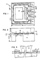
- FIGURE 1 is a top view of an exemplary hermetically sealed integrated circuit pressure sensor 10 which includes a plurality of electrical feedthrough conductors, formed in regions 12, 14 and 16, each extending across the sealed boundary area or periphery, shown at 18, between respective outside electrical contact pads or bonding pads 20, 22 and 24 and an interior sealed region 26.
- interior region 26 includes a capacitive pressure transducer region 28 and a region of on-chip electronics 30.
- Conventional integrated circuit conductors 32 e.g. thin film metal strips, connect the on-chip integrated circuit electronics 30 with the capacitive transducer region 28 and each of the feedthrough conductor regions 12, 14 and 16.
- FIGURE 2 A side view of the sensor 10 of FIGURE 1 is shown in FIGURE 2.
- a parallel plate capacitive pressure transducer 28 may be created by depositing a first metallization layer 32 on the surface 34 of a semiconductor substrate 36, and depositing a second metallization layer 38 on an opposite surface 39 of an insulator substrate or element 40 that is positioned in parallel with surface 34 and spaced a predetermined distance thereform, and forming a thin diaphragm 42 in the semiconductor substrate 36 in region 28.
- silicon is commonly used as the semiconductor substrate in integrated circuits, and Pyrex glass is preferred for use as insulator 40, since it has thermal expansion characteristics that closely matches that of silicon so as to provide the best anodic bonding therewith.
- the gap between metal plates 32 and 38 in chamber 44 may normally be on the order of 2 micrometers.
- An exemplary height for glass substrate 40 is shown as 200-500 micrometers, the thickness of diaphragm 42 may be on the order of 25 micrometers and the thickness of silicon substrate 36 may be 200-500 micrometers.
- the overall surface dimensions of sensor 10 may be 3 millimeters.
- hermetically sealed reference chamber 44 may be conventionally formed by etching a depression in the surface of glass 40 corresponding to the area or region 26 of reference chamber 44 that is to be hermetically sealed. This etching process creates glass 40 surface 39 and a mesa region 46 which extends down below the surface 39 of glass element 40. Mesa region 46 of glass element 40 defines the perimeter or periphery of the hermetically sealed region 44. To enable hermetic sealing, the mesa 46 needs to have a substantially planar surface, and the surface of the semiconductor substrate 36 on which mesa 46 rests must have a correspondingly planar surface so as to enable anodic or Mallory bonding of the two surfaces to form the hermetically sealed reference chamber 44.
- the glass element 40 is anodically bonded to the silicon substrate 36 in a vacuum so as to prevent any substantial temperature effects which otherwise would be caused by gas expansion of any remaining gas in the sealed chamber 44 after hermetic sealing had been completed.
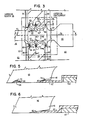
- FIGURE 3 illustrated therein is a detailed top view of an exemplary feedthrough conductor 50 according to the present invention which is in the region 12 shown in FIGURE 1. Corresponding feedthrough conductors are formed in regions 14 and 16, and are therefore not described further herein.
- FIGURE 4 shows a cross-sectional side view of the feedthrough conductor 50 viewed along the line 4-4 of FIGURE 3.
- a thick oxide layer 60 is first formed on opposide sides of the periphery 18 on top of the silicon substrate 34. Then a thinner planar oxide layer 62 is formed across periphery 18 along the predetermined path of the feedthrough conductor 50.
- a plurality of planar projections 64, 66 are formed on each side of the center line 56 of the path of said feedthrough conductor.
- planar projections are shaped to come to a point preferably at a position along a perpendicular direction with respect to center line 56 and be sufficiently sharp so as to create deformation of the glass substrate 40 against the oxide point during mallory bonding and thereby perfect a hermetic seal at this point.
- more than one projection 64, 66 is desirable to increase the reliability of the resultant seal. Only one such projection is required on each side of feedthrough conductor 50.
- Planar feedthrough conductor 50 is thereafter formed on top of the planar oxide layer 62, preferably by depositing the metal layer on the surface of the oxide in a conventional manner.
- a further projection 78 may also be formed in the metal feedthrough conductor 50 where shown in each side of the centerline 56 of the path of said conductor to provide further protection against the loss of a hermetic seal across periphery 18.
- the thick oxide 60 is formed to have a depth of about 15,000 angstroms (1.5 micrometers) and the thin oxide 62 is formed to have a thickness of 1,000 angstroms (0.1 micrometers).
- the titanium layer feedthrough conductor 50 formed on the surface of oxide layer 62 is formed to have a thickness of approximately 1,000 angstroms (0.1 micrometers).
- the portion of feedthorugh conductor 50 on opposite sides of periphery 18 is preferably thicker in regions 68 and 70, e.g., on the order of 5,000 angstroms (0.5 micrometers).
- planar metal feedthrough conductor 50 including at least one projection on each side of the conductor along the predetermined path thereof, in combination with the underlying oxide layer and its corresponding one or more projections on each side of the predetermined path of the conductor enable a hermetic seal to be formed across the periphery 18 between the interior region 26 to be hermetically sealed and the exterior environment during mallory bonding of the glass substrate 40 thereto.
- these two substrates 36, 40 can be electrostatically bonded together in a conventional manner, as above described, by first heating the glass (preferably Corning Pyrex glass) to a point where it is electrically conductive, e.g. between 300 o C and 600 o C and then applying a large DC voltage in the range of 400-2,000 volts between the two substrates 36, 40 so as to concentrate the electrostatic forces between the two substrates. It is estimated that substantial bonding forces in excess of 1,000 psi result during this bonding process.
- the glass preferably Corning Pyrex glass
- the present invention takes advantage of these large electrostatic bonding forces occurring when the surface of glass 40 is attracted into forceable intimate contact with the periphery 18 in a progressive manner to provide a seal wherein all gaps across said periphery are eliminated between the internal chamber 26 and the exterior environment.
- the forces created thereby are used to create a compression bond across the surfaces of the feedthrough conductors 50 formed across the periphery 18.
- the sealing problem in prior art devices has been that the overlying glass surface ramps over the edges of the conductors and any underlying insulator layers creating gaps or tenting regions at these edges which would extent across the bond periphery thereby creating an imperfect seal.
- the step up to the oxide 62 at the exterior side of the periphery 18 also creates a tenting region 80, but this is contiguous along the entire length of periphery 18 along most of its length, as seen in dotted line phantom in FIGURE 1, between conductors 50, such that the sharp edge of oxide layer 62 also creates a compression seal across this border of the periphery 18.
- Oxide layer 62 is formed on the external environment side of periphery 18 to ensure that no surface of silicon substrate 36 is exposed to the external environment.
- the compression bond formed across the surface of conductor 50 is sufficient to create a reliable hermetic seal
- titanium is preferably used for the feedthrough conductor 50, according to the present invention, because it also creates a electrostatic bond with the surface of glass substrate 40.
- compression bonding and electrostatic bonding of conductor 50 to the surface of glass substrate 40 also will occur only if the planar surface of conductor 50 does not have any substantial irregularities or step defects.
- the mesa 46 is about 250 micrometers across and the feedthrough conductor 50 is approximately, 150 micrometers wide at its narrowest across the periphery 18.
- FIGURE 5 illustrates a cross sectional side view of the feedthrough conductor of FIGURE 3 taken along the line 5-5.
- the mesa 46 of glass element 40 conforms its shape around the points formed on projections 72, 74 of feedthrough conductor 50 and the points formed on projections 64, 66 of oxide layer 62.
- a tenting region 80 is formed about points 72 and 74 and points 64 and 66, but, as will be seen with respect to FIGURE 7, these regions are reduced to substantially zero at the end-point of each projection.
- FIGURE 5 illustrates how the surface of glass substrate 40 is deformed during the bonding process as a result of the high electrostatic forces generated thereby.
- FIGURE 6 is a cross-sectional side view of the feedthrough conductor of FIGURE 3 taken along line 6-6. As seen in FIGURE 3, this side view is solely of the glass element 40 in contact, substantially across the entire periphery 18, with the planar surface 34 of silicon substrate 36. Only at the right-hand exterior edge of periphery 18 does the glass substrate abut against the edge of oxide layer 62, thereby creating a tenting region 80. However, the edge of oxide step 62 creates a sharp edge compression seal which prevents any air passage along this step across the length of the periphery 18.
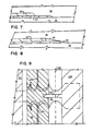
- FIGURE 7 is a cross-sectional side view of the feedthrough conductor 50 of FIGURE 3 taken along the line 7-7.
- FIGURE 7 illustrates the compressive seal forces at the farthest end point of the projections of both oxide 62 and feedthrough conductor 50.
- the pointed shapes at these end points magnifies the effective clamping forces in the vicinity thereof during electrostatic bonding, thereby increasing the deformation of the glass substrate 40 around these points and eliminate any leak path there, thereby perfecting the hermetic seal desired.
- the edge of the metal feedthrough conductor may also compress during this process since it is a deformable metal to thereby facilitate the elimination of any potential leak path at the metal oxide step. It should be realized, however, that the glass is the softest and most deformable of the various materials, mentioned above, during the mallory bonding process.
- FIGURE 8 is a cross-sectional side view of the feedthrough conductor 50 of FIGURE 3 taken along line 8-8 and illustrating the tenting regions 80 along those portions of the edge of feedthrough conductor 50 and oxide layer 62 other than at the end point of projections 72, 74 and 64, 66 respectively.
- FIGURE 9 illustrates a top view of an electrical feedthrough conductor 50 according to the present invention illustrating a preferred method of grounding the feedthrough conductor during electrostatic bonding so as to enable electrostatic bonding of the top surface of feedthrough conductor 50 to the surface of glass substrate 40 during this process.
- the diagonal cross-hatched lines at 100 represent a thin-film metal layer or plate deposited on the underside surface of glass 40. This metal layer 100 is coupled to the feedthrough conductor 50 by means of a tab 102 which extends across a line 104 of the glass substrate 40.
- Tab 102 is designed to extend down and be in intimate contact with feedthrough conductor 50 when the mesa 46 of the glass substrate 40 is placed in contact with the feedthrough conductor 50 and the surrounding periphery 18 of silicon substrate 36.
- Line 104 is a dicing line and illustrates that a portion of the glass substrate 40 indicated at 102 is cut away after electrostatic bonding so that feedthrough conductor 50 will no longer be coupled to the glass substrate metal plate 100.
- a different view of this portion 102 of glass substrate 40 is shown in phantom in FIGURE 2 at 210.
- the diagonal cross-hatched lines at 101 in FIGURE 9 represent a thin film metal layer or plate deposited on the underside surface of glass substrate 40 in the area corresponding to the interior sealed region 26 of sensor 10.
- Metal plate 101 functions to protect the on-chip electronics 30 from the high voltages that would otherwise be coupled across this integrated circuit during the electrostatic bonding process. The on-chip electronics 30 would very likely be damaged or destroyed if such a metal protection plate were not there to prevent the application of the high voltages across the circuits formed in the silicon semiconductor 36.
- Metal plate 101 may be part of metal layer 38, described previously, or may be formed separate therefrom in a conventional manner.
- the height of the chamber 44 in the area of electronics 30 may be different from the height of the chamber 44 in region 28 merely by separately etching this region of the surface of glass 40.
- the interior metal protection plate 101 is coupled to the interior surface 34 of silicon substrate 36, e.g. at the four corners of the interior region 26, so as to provide reliable contact with the silicon substrate 36 during the bonding process.
- contact between metal layers 101 and 102 may be made via the use of one of the conductors 50 as a ground conductor.
- the present invention relates in general to the formation of a hermetically sealed feedthrough conductor between an external environment and an internal hermetically sealed chamber.
- the above-described use of such a structure in a capacitive transducer, wherein a diaphragm is formed in the silicon substrate, is merely an exemplary use to show one application of the present invention. It would be obvious to one of ordinary skill in the art to apply the teachings of the present invention relating to the formation of hermetically sealed feedthrough conductors to other applications, and the present invention is envisioned as encompassing such additional applications.
Landscapes
- Physics & Mathematics (AREA)
- General Physics & Mathematics (AREA)
- Measuring Fluid Pressure (AREA)
- Pressure Sensors (AREA)
- Manufacturing Of Electrical Connectors (AREA)
- Resistance Heating (AREA)
- Ladders (AREA)
- Cylinder Crankcases Of Internal Combustion Engines (AREA)
Claims (7)
- Verfahren zum Bilden eines hermetisch geschlossenen metallischen Durchführungsleiters (50) über die planare Fläche eines Halbleitersubstrates (36), mit den Schritten(a) Bilden einer planaren Isolatorschicht (62) auf der Fläche entlang eines vorbestimmten Weges, wobei die Isolatorschicht (62) auf jeder Seite des Weges wenigstens einen planaren Vorsprung (64, 66) hat, der sich seitwärts erstreckt und so geformt ist, daß er auf einen Punkt zuläuft;(b) Bilden eines planaren metallischen Durchführungsleiters (50) auf der Oberfläche der Isolatorschicht (62) auf eine solche Weise, daß die Oberfläche der Isolatorschicht (62), die die Vorsprünge (64, 66) umfaßt, wenigstens teilweise von dem metallischen Durchführungsleiter (50) bedeckt ist, ohne die Bildung eines leitenden Weges zwischen dem Durchführungsleiter (50) und dem Halbleitersubstrat (36), wobei der Durchführungsleiter (50) dem Punkt der planaren Vorsprünge (64, 66) der Isolatorschicht (62) nächstgelegen ist, um damit im wesentlichen passende Punkte (72, 74) zu bilden;(c) Anordnen der planaren Fläche eines Isolatorelementes (40) in Kontakt mit der planaren Fläche des Halbleitersubstrates (36) und des metallischen Durchführungsleiters (50); und(d) elektrostatisches Verbinden des Isolatorelementes (40) mit dem Halbleitersubstrat (36), wobei der Punkt auf den planaren Vorsprüngen (64, 66) der Isolatorschicht (62) und des Durchführungsleiters (50) das Bilden einer Druckverbindung zwischen dem Isolatorelement (40) und dem Durchführungsleiter (50) und den freiliegenden Bereichen der Isolatorschicht (62) bewirkt.
- Verfahren nach Anspruch 1, bei dem der Schritt des Bildens einer planaren Isolatorschicht (62) den Schritt des Bildens einer Schicht aus Siliciumdioxid auf der Oberfläche des Halbleitersubstrates (36) mit einer Tiefe von etwa 0.1 Mikrometer aufweist und bei dem der Schritt des Bildens eines planaren metallischen Durchführungsleiters (50) den Schritt des Bildens einer Schicht aus Titan durch Ablagern von Titan auf der Oberfläche der Isolatorschicht (62) und mit einer Tiefe von etwa 0.1 Mikrometer aufweist.
- Verfahren nach Anspruch 1 oder Anspruch 2, bei dem das Isolatorelement ein Glassubstrat (40) ist.
- Verfahren nach einem der vorangehenden Ansprüche, bei dem das elektrostatische Verbinden bewirkt wird durch Erwärmen des Isolatorelementes (40) auf einen Punkt, an dem es elektrisch leitend ist, und Anlegen eines elektrischen Potentials über das Isolatorelement und das Halbleitersubstrat (36), während zeitweilig der Durchführungsleiter (50) extern mit dem Halbleitersubstrat (36) verbunden wird, so daß bewirkt wird, daß das Isolatorelement (40) zu innigem Kontakt mit dem Durchführungsleiter (50) und dem Halbleitersubstrat (36) angezogen wird, damit alle Lücken geschlossen werden und eine Verbindung zwischen ihnen und eine Druckversiegelung entlang der Kante der Isolatorschicht (60) gebildet wird.
- Verfahren nach Anspruch 4, bei dem eine Einrichtung zum Koppeln des Durchführungsleiters (50) mit dem Halbleitersubstrat (36) geschaffen wird durch Bilden einer leitenden Schicht auf der Oberfläche des Isolatorelementes, die bei dem Halbleitersubstrat (36) liegt, so daß der Durchführungsleiter (50) kontaktiert wird, wenn das Isolatorelement (40) dem Halbleitersubstrat (36) benachbart ist, Koppeln der leitenden Schicht an das Halbleitersubstrat (36) und, nach dem Verbinden, Entfernen der Kopplung durch würfliges Zerteilen des Isolatorelementes (40).
- Verfahren nach einem der vorangehenden Ansprüche, bei dem der metallische Durchführungsleiter (50) an der Begrenzung (18) zwischen ersten und zweiten Bereichen (20, 26) auf dem Halbleitersubstrat (36) gebildet wird, wobei der zweite Bereich (26) den ersten Bereich (20) umgibt, wobei das Isolatorelement (40) so bemessen ist, daß es den ersten Bereich (20) einschließt und eine planare Fläche hat, die an die Begrenzung (18) zwischen dem ersten und dem zweiten Bereich (20, 26) angepaßt ist und in Kontakt mit der Begrenzung (18) und mit dem metallischen Durchführungsleiter (50) ist.
- Verfahren nach einem der vorangehenden Ansprüche, bei dem das Halbleitersubstrat (36) einen darin ausgebildeten integrierten Schaltkreis umfaßt und bei dem Mittel (101) zum Schützen des integrierten Schaltkreises vor Beschädigung während des Verbindens des Isolatorelementes (40) mit dem Halbleitersubstrat (36) vorgesehen sind.
Priority Applications (1)
| Application Number | Priority Date | Filing Date | Title |
|---|---|---|---|
| AT85901155T ATE70663T1 (de) | 1984-01-25 | 1985-01-24 | Verfahren zur bildung hermetisch geschlossener elektrischer durchfuehrungsleiter. |
Applications Claiming Priority (2)
| Application Number | Priority Date | Filing Date | Title |
|---|---|---|---|
| US06/573,508 US4525766A (en) | 1984-01-25 | 1984-01-25 | Method and apparatus for forming hermetically sealed electrical feedthrough conductors |
| US573508 | 1984-01-25 |
Publications (3)
| Publication Number | Publication Date |
|---|---|
| EP0169241A1 EP0169241A1 (de) | 1986-01-29 |
| EP0169241A4 EP0169241A4 (de) | 1988-04-26 |
| EP0169241B1 true EP0169241B1 (de) | 1991-12-18 |
Family
ID=24292270
Family Applications (1)
| Application Number | Title | Priority Date | Filing Date |
|---|---|---|---|
| EP85901155A Expired - Lifetime EP0169241B1 (de) | 1984-01-25 | 1985-01-24 | Verfahren zur bildung hermetisch geschlossener elektrischer durchführungsleiter |
Country Status (6)
| Country | Link |
|---|---|
| US (1) | US4525766A (de) |
| EP (1) | EP0169241B1 (de) |
| JP (1) | JPS61501236A (de) |
| AT (1) | ATE70663T1 (de) |
| DE (1) | DE3584917D1 (de) |
| WO (1) | WO1985003381A1 (de) |
Families Citing this family (34)
| Publication number | Priority date | Publication date | Assignee | Title |
|---|---|---|---|---|
| JPH0711461B2 (ja) * | 1986-06-13 | 1995-02-08 | 株式会社日本自動車部品総合研究所 | 圧力検出器 |
| US4769622A (en) * | 1986-11-28 | 1988-09-06 | General Instrument Corporation | Reed switch having improved glass-to-metal seal |
| GB8718637D0 (en) * | 1987-08-06 | 1987-09-09 | Spectrol Reliance Ltd | Sealing electrical feedthrough |
| US4996627A (en) * | 1989-01-30 | 1991-02-26 | Dresser Industries, Inc. | High sensitivity miniature pressure transducer |
| US5164328A (en) * | 1990-06-25 | 1992-11-17 | Motorola, Inc. | Method of bump bonding and sealing an accelerometer chip onto an integrated circuit chip |
| US5513793A (en) * | 1994-10-07 | 1996-05-07 | Advanced Bionics Corporation | Brazeless ceramic-to-metal bond for use in implantable devices |
| US5738270A (en) * | 1994-10-07 | 1998-04-14 | Advanced Bionics Corporation | Brazeless ceramic-to-metal bonding for use in implantable devices |
| JP3077543B2 (ja) * | 1995-01-13 | 2000-08-14 | セイコーエプソン株式会社 | 被覆導電体およびその製造方法、およびこれを用いた電子部品、電子機器 |
| US6484585B1 (en) | 1995-02-28 | 2002-11-26 | Rosemount Inc. | Pressure sensor for a pressure transmitter |
| US5637802A (en) * | 1995-02-28 | 1997-06-10 | Rosemount Inc. | Capacitive pressure sensor for a pressure transmitted where electric field emanates substantially from back sides of plates |
| US5817984A (en) * | 1995-07-28 | 1998-10-06 | Medtronic Inc | Implantable medical device wtih multi-pin feedthrough |
| US5871513A (en) * | 1997-04-30 | 1999-02-16 | Medtronic Inc. | Centerless ground feedthrough pin for an electrical power source in an implantable medical device |
| JPH1174396A (ja) * | 1997-08-28 | 1999-03-16 | Kyocera Corp | 高周波用入出力端子ならびに高周波用半導体素子収納用パッケージ |
| US6516808B2 (en) | 1997-09-12 | 2003-02-11 | Alfred E. Mann Foundation For Scientific Research | Hermetic feedthrough for an implantable device |
| US6309494B1 (en) | 1998-12-04 | 2001-10-30 | Bridgestone/Firestone Research, Inc. | Method of attaching sensitive electronic equipment to the inner surface of a tire |
| US6244104B1 (en) | 1998-12-04 | 2001-06-12 | Bridgestone/Firestone Research, Inc. | Method for preparing an innerliner of a pneumatic tire for the quick bonding of an electronic monitoring device |
| US6508129B1 (en) | 2000-01-06 | 2003-01-21 | Rosemount Inc. | Pressure sensor capsule with improved isolation |
| DE60108217T2 (de) | 2000-01-06 | 2005-12-29 | Rosemount Inc., Eden Prairie | Kornwachstumsverfahren zur herstellung einer elektrischen verbindung für mikroelektromechanische systeme (mems) |
| US6561038B2 (en) | 2000-01-06 | 2003-05-13 | Rosemount Inc. | Sensor with fluid isolation barrier |
| US6505516B1 (en) | 2000-01-06 | 2003-01-14 | Rosemount Inc. | Capacitive pressure sensing with moving dielectric |
| US6520020B1 (en) | 2000-01-06 | 2003-02-18 | Rosemount Inc. | Method and apparatus for a direct bonded isolated pressure sensor |
| US8266465B2 (en) | 2000-07-26 | 2012-09-11 | Bridgestone Americas Tire Operation, LLC | System for conserving battery life in a battery operated device |
| US7161476B2 (en) | 2000-07-26 | 2007-01-09 | Bridgestone Firestone North American Tire, Llc | Electronic tire management system |
| ES2381940T3 (es) | 2000-07-26 | 2012-06-01 | Bridgestone Americas Tire Operations, Llc | Sistema electrónico de gestión de neumáticos |
| GB0122165D0 (en) * | 2001-09-13 | 2001-10-31 | Randox Lab Ltd | Method of sealing electrodes |
| US20030191505A1 (en) * | 2002-04-09 | 2003-10-09 | Mark Gryzwa | Magnetic structure for feedthrough filter assembly |
| US6848316B2 (en) * | 2002-05-08 | 2005-02-01 | Rosemount Inc. | Pressure sensor assembly |
| US6759309B2 (en) * | 2002-05-28 | 2004-07-06 | Applied Materials, Inc. | Micromachined structures including glass vias with internal conductive layers anodically bonded to silicon-containing substrates |
| GB2391566B (en) * | 2002-07-31 | 2006-01-04 | Schlumberger Holdings | Multiple interventionless actuated downhole valve and method |
| US7719854B2 (en) | 2003-07-31 | 2010-05-18 | Cardiac Pacemakers, Inc. | Integrated electromagnetic interference filters and feedthroughs |
| US7622782B2 (en) * | 2005-08-24 | 2009-11-24 | General Electric Company | Pressure sensors and methods of making the same |
| US7998777B1 (en) | 2010-12-15 | 2011-08-16 | General Electric Company | Method for fabricating a sensor |
| US9010200B2 (en) | 2012-08-06 | 2015-04-21 | Amphenol Thermometrics, Inc. | Device for measuring forces and method of making the same |
| WO2016176491A1 (en) * | 2015-04-28 | 2016-11-03 | Applied Materials, Inc. | Method and apparatus for fabricating battery with mesa structures and battery comprising same |
Family Cites Families (8)
| Publication number | Priority date | Publication date | Assignee | Title |
|---|---|---|---|---|
| BE590576A (de) * | 1959-05-06 | |||
| US3174112A (en) * | 1960-07-29 | 1965-03-16 | Westinghouse Electric Corp | Semiconductor devices providing the functions of a plurality of conventional components |
| US3318744A (en) * | 1963-03-27 | 1967-05-09 | Reeves Bros Inc | Method of laminating polyurethane foam |
| US4193836A (en) * | 1963-12-16 | 1980-03-18 | Signetics Corporation | Method for making semiconductor structure |
| US3386008A (en) * | 1964-08-31 | 1968-05-28 | Cts Corp | Integrated circuit |
| US3397447A (en) * | 1964-10-22 | 1968-08-20 | Dow Corning | Method of making semiconductor circuits |
| GB1138401A (en) * | 1965-05-06 | 1969-01-01 | Mallory & Co Inc P R | Bonding |
| JPS6030102B2 (ja) * | 1980-07-14 | 1985-07-15 | ヤマハ株式会社 | 半導体装置の製法 |
-
1984
- 1984-01-25 US US06/573,508 patent/US4525766A/en not_active Expired - Fee Related
-
1985
- 1985-01-24 DE DE8585901155T patent/DE3584917D1/de not_active Expired - Fee Related
- 1985-01-24 EP EP85901155A patent/EP0169241B1/de not_active Expired - Lifetime
- 1985-01-24 WO PCT/US1985/000131 patent/WO1985003381A1/en not_active Ceased
- 1985-01-24 AT AT85901155T patent/ATE70663T1/de not_active IP Right Cessation
- 1985-01-24 JP JP60500780A patent/JPS61501236A/ja active Pending
Also Published As
| Publication number | Publication date |
|---|---|
| WO1985003381A1 (en) | 1985-08-01 |
| DE3584917D1 (de) | 1992-01-30 |
| JPS61501236A (ja) | 1986-06-19 |
| ATE70663T1 (de) | 1992-01-15 |
| EP0169241A1 (de) | 1986-01-29 |
| EP0169241A4 (de) | 1988-04-26 |
| US4525766A (en) | 1985-06-25 |
Similar Documents
| Publication | Publication Date | Title |
|---|---|---|
| US4525766A (en) | Method and apparatus for forming hermetically sealed electrical feedthrough conductors | |
| US4773972A (en) | Method of making silicon capacitive pressure sensor with glass layer between silicon wafers | |
| US4530029A (en) | Capacitive pressure sensor with low parasitic capacitance | |
| US4609966A (en) | Absolute pressure transducer | |
| EP0010204B1 (de) | Halbleiter-Absolutdruck-Wandleranordnung | |
| US5243861A (en) | Capacitive type semiconductor accelerometer | |
| US4625561A (en) | Silicon capacitive pressure sensor and method of making | |
| EP0818046B1 (de) | Verfahren zur herstellung eines kapazitiven absolutdrucksensors | |
| EP0003387B1 (de) | Elektromechanischer Druckwandler | |
| US5041900A (en) | Semiconductor device having sealed electrical feedthrough | |
| US5381299A (en) | Capacitive pressure sensor having a substrate with a curved mesa | |
| US4531267A (en) | Method for forming a pressure sensor | |
| US5381300A (en) | Capacitive micro-sensor with a low stray capacity and manufacturing method | |
| EP0136249A2 (de) | Silizium-Glas-Silizium kapazitiver Druckwandler mit drei Elektroden | |
| US4612599A (en) | Capacitive pressure sensor | |
| EP0742893B1 (de) | Kapazitiver drucksensor mit einem flächenmässig begrenzten dielektrischen distanzstück | |
| US5352918A (en) | Capacitative micro-sensor with a low stray capacity and manufacturing method | |
| US6958529B2 (en) | Acceleration sensor and method of manufacture thereof | |
| US5305643A (en) | Pressure micro-sensor | |
| JPH049727A (ja) | 容量型圧力センサ | |
| US5375034A (en) | Silicon capacitive pressure sensor having a glass dielectric deposited using ion milling | |
| JPS5982753A (ja) | 半導体装置用パツケ−ジ | |
| JPH0878556A (ja) | 封止構造体 | |
| JPH08201204A (ja) | 静電容量型圧力センサ | |
| JPH07209117A (ja) | 半導体センサの封止方法及び半導体センサ |
Legal Events
| Date | Code | Title | Description |
|---|---|---|---|
| PUAI | Public reference made under article 153(3) epc to a published international application that has entered the european phase |
Free format text: ORIGINAL CODE: 0009012 |
|
| 17P | Request for examination filed |
Effective date: 19850924 |
|
| AK | Designated contracting states |
Designated state(s): AT BE CH DE FR GB LI LU NL SE |
|
| A4 | Supplementary search report drawn up and despatched |
Effective date: 19880426 |
|
| 17Q | First examination report despatched |
Effective date: 19900927 |
|
| RAP1 | Party data changed (applicant data changed or rights of an application transferred) |
Owner name: IC SENSORS, INC. |
|
| RAP1 | Party data changed (applicant data changed or rights of an application transferred) |
Owner name: CONCHA CORPORATION |
|
| GRAA | (expected) grant |
Free format text: ORIGINAL CODE: 0009210 |
|
| AK | Designated contracting states |
Kind code of ref document: B1 Designated state(s): AT BE CH DE FR GB LI LU NL SE |
|
| PG25 | Lapsed in a contracting state [announced via postgrant information from national office to epo] |
Ref country code: SE Effective date: 19911218 Ref country code: NL Effective date: 19911218 Ref country code: LI Effective date: 19911218 Ref country code: CH Effective date: 19911218 Ref country code: BE Effective date: 19911218 Ref country code: AT Effective date: 19911218 |
|
| REF | Corresponds to: |
Ref document number: 70663 Country of ref document: AT Date of ref document: 19920115 Kind code of ref document: T |
|
| REF | Corresponds to: |
Ref document number: 3584917 Country of ref document: DE Date of ref document: 19920130 |
|
| PGFP | Annual fee paid to national office [announced via postgrant information from national office to epo] |
Ref country code: NL Payment date: 19920131 Year of fee payment: 8 Ref country code: FR Payment date: 19920131 Year of fee payment: 8 |
|
| PGFP | Annual fee paid to national office [announced via postgrant information from national office to epo] |
Ref country code: GB Payment date: 19920203 Year of fee payment: 8 |
|
| PGFP | Annual fee paid to national office [announced via postgrant information from national office to epo] |
Ref country code: AT Payment date: 19920212 Year of fee payment: 8 |
|
| PGFP | Annual fee paid to national office [announced via postgrant information from national office to epo] |
Ref country code: SE Payment date: 19920214 Year of fee payment: 8 |
|
| PGFP | Annual fee paid to national office [announced via postgrant information from national office to epo] |
Ref country code: DE Payment date: 19920228 Year of fee payment: 8 |
|
| REG | Reference to a national code |
Ref country code: CH Ref legal event code: PL |
|
| PGFP | Annual fee paid to national office [announced via postgrant information from national office to epo] |
Ref country code: LU Payment date: 19920416 Year of fee payment: 8 |
|
| EN | Fr: translation not filed | ||
| PG25 | Lapsed in a contracting state [announced via postgrant information from national office to epo] |
Ref country code: FR Effective date: 19920507 |
|
| NLV1 | Nl: lapsed or annulled due to failure to fulfill the requirements of art. 29p and 29m of the patents act | ||
| PLBE | No opposition filed within time limit |
Free format text: ORIGINAL CODE: 0009261 |
|
| STAA | Information on the status of an ep patent application or granted ep patent |
Free format text: STATUS: NO OPPOSITION FILED WITHIN TIME LIMIT |
|
| EPTA | Lu: last paid annual fee | ||
| 26N | No opposition filed | ||
| PG25 | Lapsed in a contracting state [announced via postgrant information from national office to epo] |
Ref country code: LU Free format text: LAPSE BECAUSE OF NON-PAYMENT OF DUE FEES Effective date: 19930124 Ref country code: GB Effective date: 19930124 |
|
| GBPC | Gb: european patent ceased through non-payment of renewal fee |
Effective date: 19930124 |
|
| PG25 | Lapsed in a contracting state [announced via postgrant information from national office to epo] |
Ref country code: DE Effective date: 19931001 |
|
| REG | Reference to a national code |
Ref country code: FR Ref legal event code: ST |