EP0169930A1 - Enregistreur vidéo avec un milieu d'emmagasinage en forme de bande magnétique - Google Patents
Enregistreur vidéo avec un milieu d'emmagasinage en forme de bande magnétique Download PDFInfo
- Publication number
- EP0169930A1 EP0169930A1 EP84109223A EP84109223A EP0169930A1 EP 0169930 A1 EP0169930 A1 EP 0169930A1 EP 84109223 A EP84109223 A EP 84109223A EP 84109223 A EP84109223 A EP 84109223A EP 0169930 A1 EP0169930 A1 EP 0169930A1
- Authority
- EP
- European Patent Office
- Prior art keywords
- digital
- input
- output
- signal
- frequency
- Prior art date
- Legal status (The legal status is an assumption and is not a legal conclusion. Google has not performed a legal analysis and makes no representation as to the accuracy of the status listed.)
- Granted
Links
- 238000012545 processing Methods 0.000 claims abstract description 17
- 238000005070 sampling Methods 0.000 claims description 9
- 230000006870 function Effects 0.000 claims description 8
- 238000012546 transfer Methods 0.000 claims description 6
- VYZAMTAEIAYCRO-UHFFFAOYSA-N Chromium Chemical compound [Cr] VYZAMTAEIAYCRO-UHFFFAOYSA-N 0.000 claims description 5
- 238000000926 separation method Methods 0.000 claims description 5
- 239000000203 mixture Substances 0.000 claims description 4
- 230000001360 synchronised effect Effects 0.000 claims description 4
- 239000002131 composite material Substances 0.000 claims description 3
- 238000002360 preparation method Methods 0.000 claims 1
- 230000010354 integration Effects 0.000 abstract description 3
- 238000012986 modification Methods 0.000 abstract description 3
- 230000004048 modification Effects 0.000 abstract description 3
- 238000006243 chemical reaction Methods 0.000 abstract 1
- 238000010586 diagram Methods 0.000 description 19
- 235000012239 silicon dioxide Nutrition 0.000 description 5
- 230000008901 benefit Effects 0.000 description 4
- 239000010453 quartz Substances 0.000 description 4
- VYPSYNLAJGMNEJ-UHFFFAOYSA-N silicon dioxide Inorganic materials O=[Si]=O VYPSYNLAJGMNEJ-UHFFFAOYSA-N 0.000 description 4
- 230000001419 dependent effect Effects 0.000 description 3
- 230000002349 favourable effect Effects 0.000 description 3
- 238000000034 method Methods 0.000 description 3
- 230000008569 process Effects 0.000 description 3
- 230000005540 biological transmission Effects 0.000 description 2
- 230000008878 coupling Effects 0.000 description 2
- 238000010168 coupling process Methods 0.000 description 2
- 238000005859 coupling reaction Methods 0.000 description 2
- 238000005516 engineering process Methods 0.000 description 2
- 230000001629 suppression Effects 0.000 description 2
- 230000003321 amplification Effects 0.000 description 1
- 238000012937 correction Methods 0.000 description 1
- 239000013078 crystal Substances 0.000 description 1
- 230000003247 decreasing effect Effects 0.000 description 1
- 230000006735 deficit Effects 0.000 description 1
- 238000011161 development Methods 0.000 description 1
- 230000018109 developmental process Effects 0.000 description 1
- 230000009977 dual effect Effects 0.000 description 1
- 230000000694 effects Effects 0.000 description 1
- 230000005669 field effect Effects 0.000 description 1
- 238000001914 filtration Methods 0.000 description 1
- 238000003199 nucleic acid amplification method Methods 0.000 description 1
- 230000010363 phase shift Effects 0.000 description 1
- 230000008929 regeneration Effects 0.000 description 1
- 238000011069 regeneration method Methods 0.000 description 1
- 230000009897 systematic effect Effects 0.000 description 1
Images

Classifications
-
- H—ELECTRICITY
- H04—ELECTRIC COMMUNICATION TECHNIQUE
- H04N—PICTORIAL COMMUNICATION, e.g. TELEVISION
- H04N9/00—Details of colour television systems
- H04N9/79—Processing of colour television signals in connection with recording
-
- H—ELECTRICITY
- H04—ELECTRIC COMMUNICATION TECHNIQUE
- H04N—PICTORIAL COMMUNICATION, e.g. TELEVISION
- H04N9/00—Details of colour television systems
- H04N9/79—Processing of colour television signals in connection with recording
- H04N9/7921—Processing of colour television signals in connection with recording for more than one processing mode
- H04N9/7925—Processing of colour television signals in connection with recording for more than one processing mode for more than one standard
-
- H—ELECTRICITY
- H04—ELECTRIC COMMUNICATION TECHNIQUE
- H04N—PICTORIAL COMMUNICATION, e.g. TELEVISION
- H04N9/00—Details of colour television systems
- H04N9/79—Processing of colour television signals in connection with recording
- H04N9/80—Transformation of the television signal for recording, e.g. modulation, frequency changing; Inverse transformation for playback
- H04N9/82—Transformation of the television signal for recording, e.g. modulation, frequency changing; Inverse transformation for playback the individual colour picture signal components being recorded simultaneously only
- H04N9/83—Transformation of the television signal for recording, e.g. modulation, frequency changing; Inverse transformation for playback the individual colour picture signal components being recorded simultaneously only the recorded chrominance signal occupying a frequency band under the frequency band of the recorded brightness signal
- H04N9/831—Transformation of the television signal for recording, e.g. modulation, frequency changing; Inverse transformation for playback the individual colour picture signal components being recorded simultaneously only the recorded chrominance signal occupying a frequency band under the frequency band of the recorded brightness signal using intermediate digital signal processing
Definitions
- the invention relates to a video recorder with a magnetic tape-shaped storage medium, in which, after the chroma signal has been separated from the demodulated color-picture-blanking-synchronous signal mixture, that is to say from the composite signal, the chroma signal is converted to a carrier signal with a carrier frequency that is lower than the standard color carrier frequency.
- the picture blanking-synchronous signal mixture i.e.
- the BAS signal is subjected to frequency modulation and the sum of the carrier-frequency-reduced chroma signal and the frequency-modulated BAS signal is stored in the storage medium by means of a head system and, from there, by means of the head system removed again and then transformed back into the CVBS signal, and with control circuits of the motors of the tape-shaped storage medium and the head system.
- T he ( "unte r e") color carrier frequency is for the VHS system at the PAL standard 627 kHz and at the NTSC standard 629 kHz, with the former frequency, the 40.125-fold, and the second is 40 times the respective horizontal Deflection frequency of PAL or NTSC is.
- the coupling of these carrier frequencies with the respective horizontal deflection frequency makes it possible during playback to compensate fluctuations in the speed of the tape-shaped storage medium so precisely that a phase-accurate regeneration of the original color carrier frequency can be achieved. * ) low
- the solution of this overall task according to the invention is initially based on the idea of performing the signal processing required in the respective video recorder system by means of fast digital circuits, but not storing the output signals of these digital circuits digitally on the tape-shaped storage medium, but instead converting them back into corresponding analog signals before the storage.
- a fast analog-to-digital converter is thus provided, the scanning signal of which has a constant frequency that is uniform for all three color television standards.
- the invention is based on the further idea of * carrying out the aforementioned digital signal processing at an intermediate carrier frequency which is constant for all three color television standards and which is an integer subharmonic of the scanning signal frequency. *) in the chrome channel
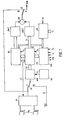
- Fig. 1 shows a schematic block diagram for a general embodiment of the invention.
- the analog input of the fast analog-digital converter aw is located via the first switch u1 either in recording mode R at the composite signal input fse or in playback mode P at the output of the two-direction amplifier arrangement zv for the head system ks, of which two heads are shown schematically are shown.
- the analog-to-digital converter aw since it is expressly intended to be a faster one, is preferably a so-called flash converter, at the output of which a parallel digital word, which has several digits in accordance with its resolution, occurs at the frequency of the frequency Fc of its scanning signal fc.
- sampling oscillator os which oscillates at a fixed frequency for all three color television standards, PAL, NTSC, SECAM. According to a preferred embodiment, this frequency is in the range of about 18 to 20 MHz, e.g. at 18M3z.
- the mentioned digital words occurring at the output of the digital converter aw are thus the digitized CVBS signal fs' in the recording mode R.
- This is now done in three high-speed digital circuits db, dc, dm x) which are mutually in data traffic.
- the digital circuit db essentially takes over the processing of the BAS signal and the separation of the synchronous signals from the BAS signal, so that pure digital luminance signals Y ultimately appear at their output.
- the chroma signal cs can be separated by means of the digital circuit db and is further processed in accordance with the standards in the digital circuit dc.
- the digital circuit dm generates control signals sm for the motors of the head or belt drive and also receives corresponding correction signals cr.
- the three fast digital circuits db, dc, dm are also operated on the frequency-constant scanning signal fc. x) processed with at least partially parallel signal processing.
- the control unit se operated on the scanning signal fc is connected on the one hand to the control elements of the video recorder and on the other hand forwards the signals or commands coming from there to the fast digital circuits db, dc, dm.
- dc is the first or second digital-to-analog converter dw1, dw2, whose respective output signal is generated by means of the analog adder aa in the aforementioned analog signal for storage on the magnetic storage medium. Its output is thus via the second switch u2 during recording operation R on the amplifier zv, the amplification properties of which can be controlled by the digital circuit d b as a function of recording / playback via the line vl.
- playback mode P the input of the analog-digital converter aw is connected to the amplifier zv via the first switch u1 and the output of the analog adder aa is connected to the CVBS output fsa via the second switch u2.
- Fig. 1 a distinction is drawn between the lines with analog signals and those with digital signals by the graphical representation of the cable routing. While the former are drawn as simple lines, the latter are strip-like buses that consist of at least as much parallel lines as the digits to be processed have digits.
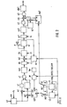
- FIG. 2 shows the block diagram of an exemplary embodiment for the chrominance signal processing, the circuit diagram beginning with the signal flow for the sake of completeness and for ease of understanding in terms of signal flow with the analog-digital converter aw, which receives its input signal from the first switch u1.
- the circuit shown in Fig. 2 is used for both recording and playback operation, only individual operating parameters are switched, but not the direction of signal flow.
- the output of the analog-digital converter aw is at the first input of the first and the second digital multiplier m1, m2, the respective second input of which is connected to the sine or cosine output sa, ca of the first digital frequency-adjustable and controllable sine generator sg1 .
- the output of the first multiplier m1 is via the first digital delay element v1, the delay of which is equal to that of the first digital 90 ° phase shifter h1, at the first input and the output of the second multiplier m2 is via the first 90 ° phase shifter h1 at the second input of the first digital adder a1.
- the frequency setting input fe of the first sine generator sg1 for the VHS system during recording operation R is the first digital signal ds1, which is the difference between a quarter of the scanning signal frequency F1 and the respective color carrier frequency, or during reproduction P the second digital signal ds2, which is the sum of a quarter of the scanning signal frequency Fc and corresponds to 40 times with the NTSC standard or with PAL or x) .
- the associated color carrier frequency or horizontal frequency is thus input into the first sine generator sg1. This is indicated in FIG.
- the two registers r1, r2 which contain or calculate the specified digital signals ds1, ds2 and emit them in accordance with the set standard, as indicated by the input marked with the three standard designations PAL, NTSC, SECAM .
- the horizontal register pulse ss is also fed to the second register r2.
- the different connection of the digital signals ds1, ds2 to the sine oscillators sg1, sg2 during recording or playback is done by means of the third and fourth electronic switch u3, u4.
- the digital signals ds1, ds2 are to be selected in the Video 2000 or Betamax system according to the associated frequency of the "lower" color subcarrier.
- the subcircuit consisting of the two multipliers m1, m2, the delay element v1, the 90 ° phase shifter h1, the adder a1 and the digital sine generator sg1 represents a digital quadrature mixer with which the color carrier frequency of the CVBS signal is exactly set in all three color television standards A quarter of the sampling frequency Fc is shifted, which frequency in the exemplary embodiment according to FIG. 2 is the intermediate carrier frequency zt.
- the output of the adder a1 is at the input of the standard band pass nb1, the pass band of which is set according to the respective color television standard. Like the two registers r1, r2, it also has a corresponding setting input, which, however, is not shown in FIG. 2 for reasons of simplification.
- the output of the standard bandpass filter nb1 is via the digital decimator dz, whose scanning signal frequency F1 is equal to one third of the scanning signal frequency, at the first input of the third multiplier m3. Its output is connected to the input of the digital forming band pass fb, the output of which is connected via the digital comb filter kf to the input of the first digital interpolator ip1 clocked by the scanning signal fc.
- the switch By means of the switch it, which is closed during recording mode R, it is achieved that the digital comb filter kf is only effective during the playback mode P.
- decimator dz and the first interpolator ip1 By means of the decimator dz and the first interpolator ip1, it is achieved for those subcircuits which process and process the chroma signal that they cannot work with the high scanning signal frequency Fc, but with a cheaper, lower clock frequency. As a result, there is sufficient time available for this processing and the amount of memory for the comb filter kf drops considerably.
- the output of the interpolator ip1 lies via the second digital standard bandpass nb2 and the second digital delay element v2 connected downstream thereof, the delay time of which is equal to that of the second 90 ° phase shifter h2, at the first input of the fourth digital multiplier m4 and via the second standard band Bandpass nb2 at the input of the second 90 ° phase shifter h2, the output of which at the first input of the fifth digital multiplier m5 is connected.
- the second input of the fourth and fifth multiplier m4, m5 is connected to the cosine and sine output ca, sa of the second digital frequency-adjustable sine generator sg2, while their outputs are connected via the second adder a2 to the input of the first digital-to-analog converter dw1 are.
- the frequency setting input fe of the second sine generator sg2 is supplied with the above-mentioned second digital word ds2 in recording mode R and the above-mentioned first digital word ds1 in playback mode P.
- the delay element v2, the 90 ° phase shifter h2, the two multipliers m4, m5, the adder a2 and the sine generator sg2 likewise form, like the corresponding subcircuits v1, h1, m1, m2, a1, arranged behind the analog-digital converter aw.
- the two signals to be mixed and phase-shifted by exactly 90 ° are first generated, which are then combined with the cosine or sine signal of the sine oscillator sg2 are mixed and then added, the first quadrature mixer with the subcircuits first mixes the input signal with the sine or cosine signal of the sine oscillator and only then generates the 90 ° phase-shifted signal from the cosine-multiplied signal.
- the first sine generator sg1 also has the phase control input fr, which is connected to the output of the digital phase control circuit pr, which compares the digital horizontal synchronizing signal ss with the signal from the digital horizontal oscillator ho.
- the sine generator sg1 is thus comparable to an analog PLL oscillator and has a frequency stability that corresponds to that of a conventional quartz oscillator.
- the second input of the third multiplier m3 is located at the output of the digital automatic color control stage ac, the signal input of which is connected to the output of the comb filter kf and the clock input of which is supplied with the synchronization pulses ss.
- the color control stage ac regulates the amplitude of the color burst signal to a constant value in order to optimally control the magnetic storage medium when recording, or amplitude fluctuations during playback, e.g. due to varying tape properties. Furthermore, the color control stage itself ensures that the color burst signal itself is boosted and decreased in accordance with the standards.
- two heads are usually used, which are alternately in contact with the storage medium.
- the control variables for the two heads are then advantageously determined separately in the color control stage ac in order to compensate for systematic differences between the two transmission paths.
- the color control stage is supplied with a further signal, not shown, which denotes the head that is currently in contact with the strip.
- the comb filter kf increases the crosstalk attenuation between adjacent tracks of the storage medium during playback using the usual phase advance of the chroma signal when recording.
- the phase of the chroma signal is changed line by line in such a way that the crosstalk components are compensated for when reproduced in a suitable comb filter.
- these phase changes are caused by corresponding signals at the frequency input fe of the sine generator sg2, or are reversed when the frequency input of the sine generator sg1 is reproduced.
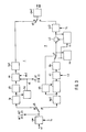
- FIG. 3 shows the block diagram of an exemplary embodiment for processing the BAS signal.
- the first subchannel r serves the recording mode R and the second subchannel p serves the playback mode P.
- the scanning signal fc is again used, the constant frequency Fc of which is preferably around 18 to 20 MHz, i.e. the analog-digital converter aw is again assumed.
- its output signal is also the fifth electronic switch ter. u5 supplied, which supplies either sub-channel r or sub-channel p according to the selected operating mode R, P.
- the output signal of the analog-digital converter aw is at the input of the low-pass filter tp, whose upper cut-off frequency is approximately 3 MHz and whose output feeds the digital synchronous pulse isolating stage ha and via the digital pre-emphasis and limiter stage pb with the input of the digital voltage-controlled Oscillator vo is connected as a frequency modulator.
- This is supplied with the third digital word ds3, which determines the carrier frequency and is dependent on the television standard.
- the output of the oscillator vo is connected to the input of the second digital-to-analog converter dw2 via the first digital high-pass filter hp1, the lower limit frequency of which is approximately 1.5 MH z, and the sixth electronic switch u6.
- the output signal of the analog-digital converter aw is fed via the changeover switch u5 to the second digital high-pass filter hp2, whose lower limit frequency is approximately 1.5 MHz and whose output is coupled to the input of the second digital-analog converter dw2 is.
- the output of the frequency demodulator fd is connected to the input of the digital decimating low-pass filter dt, the upper limit frequency of which is approximately 3 MHz and to which the clock signal f2 with half the scanning signal frequency FC / 2 is supplied, so that the digital words at its output in time with this clock frequency F2 occur.
- the digital de-emphasis and noise suppression stage du At the output of the decimating low-pass filter dt is the digital de-emphasis and noise suppression stage du, the output of which on the one hand via the first input-output path of the seventh electronic switch u7 to the first input of the third adder a3 and on the other hand via the second input-output path of the switch u7 am first input of the digital correlator kl, the second input of which is connected to the output of the third adder a3 and the output of which is connected to the second input of this adder a3.
- the output of the switch u7 is also at the input of the delay stage vs, whose delay time is equal to one picture line duration of the television system.
- the second digital interpolator ip2 clocked by the scanning signal fc the output of which is via the sixth electronic switch u6 is connected to the input of the second digital-to-analog converter dw2.
- the control input of the switch u7 is finally at the output of the dropout detector dk, the input of which is fed by the output of the second high pass hp2.
- the dropout detector dk consists of a comparison circuit which actuates the changeover switch u7 when the input level falls below a predetermined level, so that the signal from the previous medium is substituted for the weak and consequently very noisy signal from the storage medium Image line is taken from the delay stage vs.
- Correlator kl is also used for noise suppression. In this customary circuit, noise is suppressed by filtering when the signals of successive image lines are slightly different, while when there is a large difference the filter is switched off (“motion detector”) in order to counteract undesired impairment of rapid, vertical image changes.
- FIG. 4 shows the block diagram of a preferred embodiment for the frequency demodulator fd according to FIG. 4. Its input is via the third delay element v3, the delay time of which is equal to that of the third digital 90 ° phase shifter h3, and the first digital amount generator bb1 connected downstream of it at the subtrahend input s of the subtractor st and at the first signal input of the electronic multiple switch kr.
- the third 90 ° phase shifter h3 lies between the input of the frequency demodulator and that of the second digital absolute value generator bb2, the output of which is connected to the minuend input m of the subtractor st and to the second signal input of the multiple cross switch kr.
- Its control input is connected to the output va of the subtractor st, which carries the sign signal, and its two signal outputs are at the dividend or divider input dd, dr of the digital divider d, the output of which is connected to the address input of the one containing the arctangent values of the first half quadrant Read-only memory rm is connected.
- the most significant digit of the output signal of the third delay element v3 and the third 90 ° phase shifter h3 is fed to the first and the second input of the first antivalence element ex1, the output of which is at the first input of the second antivalence element ex2 and the second input of the sign output of Subtractor st is connected.
- Each output of the read-only memory rm is followed by one of the inverters of the first multiple inverter vi1, the respective inputs of which are connected to the respective first input of the individual changeover switches of the first multiple changeover switch vu1.
- Their respective second inputs are connected to the respective output of the read-only memory rm, and the common control input of the individual changeover switches is at the output of the second antivalence element ex2, while the digital differentiator dg is connected downstream of the first output of the multiple changeover switch vu1.
- the positions of the output signal of the multiple switch (vu) are supplemented on the higher value side by the output of the second antivalence element ex2 as the next higher position, the output of the first antivalence element ex1 as the second higher position and the sign position of the output signal of the third delay element v3 as the highest position.
- the output of the multiple switch (vu) is followed by the digital differentiator dg.
- the read-only memory rm only needs to contain those arctangent values that lie in the first half-quadrant, that is between 0 ° and 45 °. This makes this read-only memory optimally small.
- the additional number of digits with the associated signals which are required for a full angle of 360 ° are added to the output signal of the read-only memory rm.
- the phase-demodulated signal of the input signal to be frequency-modulated is therefore already present at the output of the multiple switch vu1, and the frequency-demodulated signal is obtained therefrom by means of the differentiating element dg.
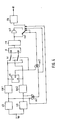
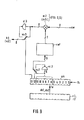
- FIG. 5 shows a further development of the arrangement according to FIG. 2, which contains additional subcircuits for SECAM operation. Specifically, it is provided that the first digital filter df1 is arranged at the output of the first standard bandpass pass nb1, the filter characteristics of which can be switched from bell-shaped during recording operation to inverse-bell-shaped during playback, which switching is again not shown in FIG. 5 for the sake of simplicity.
- the further digital frequency demodulator fd ' is connected, which is followed by the digital frequency modulator fm, the stroke of which can be switched from a first value during recording operation to a second value during playback and which can only be switched on during the by means of the horizontal synchronizing pulse ss Times with a chroma signal is activated.
- the frequency modulator fm is followed by the second digital filter df2, the filter characteristics of which can be switched from bell-shaped during playback to inverted-bell-shaped during recording operation (switchability is not shown again) and whose output is only available with SECAM operation via the first input-output path of the eighth electronic switch u8 is connected to the entrance of the second standard band pass nb2.
- the second output path of the switch u8 connects the output of the first interpolator ip1 to the input of the second standard bandpass filter nb2.
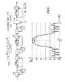
- Fig. 6 shows the block diagram and the frequency characteristic for the preferred dimensioning of the first standard bandpass filter nb1.
- the digital filter shown in FIG. 6 has a very favorable structure with regard to the number of addition stages ad and subtraction stages sb used.
- Its transfer function H (z) is the following:
- the digital filter according to FIG. 6 is composed of the already mentioned addition stages ad, the subtraction stage sb and retarders v, the delay time of which corresponds to a multiple of the period of the scanning signal of the filter, this multiple being the positive number in the exponent of the base z corresponds.
- the term (1 + z-6) is realized in that the associated circuit part is arranged behind the decimator dz in terms of signal flow, whose scanning signal f1 has a frequency F1 equal to one third of the frequency F c of the Sampling signal fc. At a frequency Fc of 18 MHz, this circuit part is therefore operated at a frequency Fc / 3 of 6 MHz.
- the delay element of the circuit part with the symbol z * and the exponent -2 arranged behind the decimator dz has a delay time of 2Fc / 3, which is 6Fc.
- the frequency characteristic shown in FIG. 6 indicates the normalized attenuation g in the attenuation measure dB above the frequency F in MHz.
- the maximum of the curve is 4.5 MHz corresponding to the intermediate carrier frequency mentioned above.
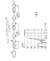
- this digital filter also has multiplier stages mp which allow the constant decimal factor 0.375 of the transfer function H (z) to take effect. This is as follows:
- This digital filter in turn has a favorable structure in terms of the number of addition and subtraction stages. Its filter characteristic is symmetrical to 1.5 MHz, which results from the fact that this filter is clocked with the scanning signal f1 of the frequency Fc / 3 and thus the intermediate carrier frequency of 4.5 MHz is also shifted to a third.
- the digital multiplexer mx is arranged at the input of the digital filter according to FIG. 8 and generates the sequence of three e, 0, -e from each input digital word e. This sequence of three corresponds to the realization of the term (1-z -2 ).
- the graphical representation of the frequency characteristic of the digital filter according to FIG. 8 is interrupted or compressed between 3.0 MHz and 4.0 MHz. This digital filter is clocked with the sampling signal fc, so that the attenuation minimum (0 dB) is 4.5 MHz if a sampling frequency Fc of 18 MHz is again assumed.
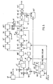
- FIG. 9 shows the block diagram for a preferred embodiment of the two sine generators sg1, sg2 * according to FIG. 2.
- Accumulators are known to be clock-accumulating circuits which add the same number to the result of the previous clock pulse for each clock pulse.
- One of the two digital words ds1, ds2 from one of the two registers r1, r2 according to FIG. 2 or 5 is thus located at the frequency setting input fe.
- the scanning signal fc is supplied to the accumulator ak as a clock signal. * ) with multiplier m2 or m5 for mixing
- the respective input of the individual inverters is located at the respective first input of the individual changeover switches of the second multiple changeover switch vu2, while their respective second input is connected to the respective output for the q digits and the common control input of the individual changeover switches at the output of (j-1) - position.
- the output of the second multiple switch vu2 is connected to the address input of the further read-only memory rm 'containing the sine values of the first quadrant, the output of which is at the first input of one of the multipliers m2, m5.
- Its second input is the signal input and one of the inverters of the third multiple inverter vi3 is connected to its output, the respective inputs of which are connected to the respective first input of the individual changeover switches of the third multiple changeover switch vu3, while their respective second input is connected to the output of the multiplier m2 or m5 is connected.
- the common control input of the individual changeover switches of the third multiple changeover switch vu3 is located at the output of the jth position of the accumulator ak, and the output of the third multiple changeover switch v u3 supplies the input signal multiplied by the sine signal.
- the sine values of the second to fourth quadrants can also be generated using the sine values of the first quadrant contained in the read-only memory rm '.
- the cosine values at the respective cosine output ca of the sine generators sg1, sg2 can be generated in a similar and analogous manner, not shown in FIG. 9.
- a further read-only memory as well as another two multiple inverters and another two lots can be used subject changeover switch are provided.
- the invention can be implemented by means of monolithically integrated circuits, as has already been mentioned at the beginning, wherein the overall circuit can be assigned to a single monolithically integrated circuit or divided into several if necessary. Since the individual subcircuits are all digital circuits, the implementation by means of insulating layer field effect transistors, that is to say in the so-called MOS technology, is particularly favorable, but fast bipolar digital circuit technologies can also be suitable for implementation.
- the principle used in the chrome channel, using quadrature mixing, to shift the digital processing to a subharmonic of the clock frequency independently of the standard-dependent color carrier frequency and thus to be able to work with a fixed sampling frequency in all color television standards, has the great advantage of only having a single clock generator with a fixed frequency for the sampling signal to have to provide. Since this is usually a quartz oscillator, only a single quartz is required, while three quartz oscillators (one each for PAL, NTSC, SECAM) or an oscillator with switchable three quartzes would be required if its frequency were "connected" to the standard-dependent fourfold color carrier frequency.
- the application of this principle is therefore not limited to video recorders, but it can be used successfully wherever color television signals of several standards are to be digitized.
Landscapes
- Engineering & Computer Science (AREA)
- Multimedia (AREA)
- Signal Processing (AREA)
- Television Signal Processing For Recording (AREA)
Priority Applications (4)
| Application Number | Priority Date | Filing Date | Title |
|---|---|---|---|
| EP84109223A EP0169930B1 (fr) | 1984-08-03 | 1984-08-03 | Enregistreur vidéo avec un milieu d'emmagasinage en forme de bande magnétique |
| DE8484109223T DE3464189D1 (en) | 1984-08-03 | 1984-08-03 | Videorecorder with a magnetic tape storage medium |
| US06/760,396 US4757390A (en) | 1984-08-03 | 1985-07-30 | Video recorder with a magnetic recording medium in the form of a tape |
| JP60170995A JPH0683476B2 (ja) | 1984-08-03 | 1985-08-02 | ビデオ処理回路 |
Applications Claiming Priority (1)
| Application Number | Priority Date | Filing Date | Title |
|---|---|---|---|
| EP84109223A EP0169930B1 (fr) | 1984-08-03 | 1984-08-03 | Enregistreur vidéo avec un milieu d'emmagasinage en forme de bande magnétique |
Publications (2)
| Publication Number | Publication Date |
|---|---|
| EP0169930A1 true EP0169930A1 (fr) | 1986-02-05 |
| EP0169930B1 EP0169930B1 (fr) | 1987-06-10 |
Family
ID=8192093
Family Applications (1)
| Application Number | Title | Priority Date | Filing Date |
|---|---|---|---|
| EP84109223A Expired EP0169930B1 (fr) | 1984-08-03 | 1984-08-03 | Enregistreur vidéo avec un milieu d'emmagasinage en forme de bande magnétique |
Country Status (4)
| Country | Link |
|---|---|
| US (1) | US4757390A (fr) |
| EP (1) | EP0169930B1 (fr) |
| JP (1) | JPH0683476B2 (fr) |
| DE (1) | DE3464189D1 (fr) |
Cited By (6)
| Publication number | Priority date | Publication date | Assignee | Title |
|---|---|---|---|---|
| EP0245532A1 (fr) * | 1986-05-10 | 1987-11-19 | Deutsche ITT Industries GmbH | Circuit numérique pour le traitement d'un signal de télévision couleur |
| US4994754A (en) * | 1988-05-24 | 1991-02-19 | Matsushita Electric Industrial Co., Inc. | Digital FM demodulating apparatus |
| US5051614A (en) * | 1988-05-26 | 1991-09-24 | Matsushita Electric Industrial Co., Ltd. | Dropout detecting apparatus |
| US5062004A (en) * | 1988-02-26 | 1991-10-29 | Deutsche Itt Industries Gmbh | Digital signal processing circuit for video tape recorder |
| EP0177320B1 (fr) * | 1984-09-29 | 1992-03-11 | Victor Company Of Japan, Limited | Système de traitement numérique du signal vidéo |
| EP0820201A3 (fr) * | 1996-07-18 | 1999-05-26 | Philips Patentverwaltung GmbH | Circuit de conversion de fréquence d'un signal couleur |
Families Citing this family (29)
| Publication number | Priority date | Publication date | Assignee | Title |
|---|---|---|---|---|
| JPS6170880A (ja) * | 1984-09-14 | 1986-04-11 | Matsushita Electric Ind Co Ltd | ビデオ信号の記録処理方法 |
| KR890015245A (ko) * | 1988-03-30 | 1989-10-28 | 무라가미 류우이찌 | 비디오신호의 휘도 및 색성분으로부터 분리클록신호를 획득하는 자기 기록재생 장치 |
| DE68928197T2 (de) * | 1988-12-23 | 1997-12-11 | Matsushita Electric Ind Co Ltd | Videobandrekorder mit Fernsehnormwandler |
| JP2797393B2 (ja) * | 1989-04-10 | 1998-09-17 | キヤノン株式会社 | 記録再生装置 |
| US5504532A (en) * | 1989-09-07 | 1996-04-02 | Advanced Television Test Center, Inc. | Bi-directional television format digital signal converter with improved luminance signal-to-noise ratio |
| US5280397A (en) * | 1989-09-07 | 1994-01-18 | Advanced Television Test Center, Inc. | Bi-directional HDTV format digital signal converter |
| JPH03101486A (ja) * | 1989-09-14 | 1991-04-26 | Hitachi Ltd | 映像信号記録再生方法及び装置 |
| JP2954328B2 (ja) * | 1990-06-27 | 1999-09-27 | 株式会社日立製作所 | 映像信号の記録再生装置 |
| DE69122338T2 (de) * | 1990-08-03 | 1997-02-13 | Canon Kk | Synchronsignal-Detektorschaltung und dieselbe enthaltender Synchronsignal-Detektorapparat |
| US6718122B1 (en) * | 1991-01-18 | 2004-04-06 | Canon Kabushiki Kaisha | Image processing apparatus |
| KR930010485B1 (ko) * | 1991-09-17 | 1993-10-25 | 삼성전자 주식회사 | 자막정보 처리장치 |
| TW232739B (fr) * | 1991-12-16 | 1994-10-21 | Sony Co Ltd | |
| US5804741A (en) * | 1996-11-08 | 1998-09-08 | Schlumberger Industries, Inc. | Digital phase locked loop signal processing for coriolis mass flow meter |
| US6233287B1 (en) * | 1997-04-04 | 2001-05-15 | Motorola, Inc. | Method and apparatus for mixing signals |
| US7784360B2 (en) | 1999-11-22 | 2010-08-31 | Invensys Systems, Inc. | Correcting for two-phase flow in a digital flowmeter |
| US6311136B1 (en) * | 1997-11-26 | 2001-10-30 | Invensys Systems, Inc. | Digital flowmeter |
| US20030216874A1 (en) * | 2002-03-29 | 2003-11-20 | Henry Manus P. | Drive techniques for a digital flowmeter |
| US8447534B2 (en) | 1997-11-26 | 2013-05-21 | Invensys Systems, Inc. | Digital flowmeter |
| US7124646B2 (en) * | 1997-11-26 | 2006-10-24 | Invensys Systems, Inc. | Correcting for two-phase flow in a digital flowmeter |
| US8467986B2 (en) * | 1997-11-26 | 2013-06-18 | Invensys Systems, Inc. | Drive techniques for a digital flowmeter |
| US7404336B2 (en) | 2000-03-23 | 2008-07-29 | Invensys Systems, Inc. | Correcting for two-phase flow in a digital flowmeter |
| DE01918944T1 (de) * | 2000-03-23 | 2004-10-21 | Invensys Systems, Inc., Foxboro | Korrektur für eine zweiphasenströmung in einem digitalen durchflussmesser |
| JP3621345B2 (ja) * | 2000-12-12 | 2005-02-16 | Necエレクトロニクス株式会社 | 複数のテレビジョン信号方式に対応可能な映像信号処理回路 |
| US7971225B2 (en) * | 2002-02-08 | 2011-06-28 | Finisar Corporation | Bandpass component decimation and transmission of data in cable television digital return path |
| US7042518B1 (en) * | 2002-04-29 | 2006-05-09 | National Semiconductor Corporation | Digitally controlled variable frequency HF emphasis circuit for use in video displays |
| US7059199B2 (en) * | 2003-02-10 | 2006-06-13 | Invensys Systems, Inc. | Multiphase Coriolis flowmeter |
| US7188534B2 (en) * | 2003-02-10 | 2007-03-13 | Invensys Systems, Inc. | Multi-phase coriolis flowmeter |
| US7065455B2 (en) * | 2003-08-13 | 2006-06-20 | Invensys Systems, Inc. | Correcting frequency in flowtube measurements |
| US7617055B2 (en) | 2006-08-28 | 2009-11-10 | Invensys Systems, Inc. | Wet gas measurement |
Family Cites Families (9)
| Publication number | Priority date | Publication date | Assignee | Title |
|---|---|---|---|---|
| JPS56158581A (en) * | 1980-05-10 | 1981-12-07 | Victor Co Of Japan Ltd | Recording and playback system for rotating recording medium |
| JPS58186279A (ja) * | 1982-04-23 | 1983-10-31 | Sony Corp | デジタルvtr |
| NL8301013A (nl) * | 1983-03-22 | 1984-10-16 | Philips Nv | Kleurentelevisie transmissie- respektievelijk informatieopslagsysteem met tijdmultiplexkodering en daartoe geschikte informatiegever en -ontvanger. |
| GB2140644B (en) * | 1983-05-17 | 1986-09-17 | Sony Corp | Television standards converters |
| US4583113A (en) * | 1983-08-26 | 1986-04-15 | Rca Corporation | Progressive scan television display system employing interpolation in the luminance channel |
| US4633293A (en) * | 1983-09-26 | 1986-12-30 | Rca Corporation | High definition television signal for film-television standards conversion system |
| JPS60111591A (ja) * | 1983-11-21 | 1985-06-18 | Victor Co Of Japan Ltd | カラ−映像信号の記録方法及び記録再生方法 |
| US4593315A (en) * | 1984-05-29 | 1986-06-03 | Rca Corporation | Progressive scan television receiver for non-standard signals |
| US4652906A (en) * | 1985-03-12 | 1987-03-24 | Racal Data Communications Inc. | Method and apparatus for color decomposition of video signals |
-
1984
- 1984-08-03 EP EP84109223A patent/EP0169930B1/fr not_active Expired
- 1984-08-03 DE DE8484109223T patent/DE3464189D1/de not_active Expired
-
1985
- 1985-07-30 US US06/760,396 patent/US4757390A/en not_active Expired - Fee Related
- 1985-08-02 JP JP60170995A patent/JPH0683476B2/ja not_active Expired - Lifetime
Non-Patent Citations (3)
| Title |
|---|
| GRUNDIG TECNISCHE INFORMATIONEN, vol. 30, no. 2, 1983, Seiten 79-81, Regensburg, DE; G. REIME: "Der Chromabaustein der neuen Videorecorder" * |
| IEEE TRANSACTIONS ON CONSUMER ELECTRONICS, Band CE-26, Nr. 3, August 1980, Seiten 315-321, New York, US; I. NAKAGAWA u.a.: "New chrominance signal processing LSI for home VCR" * |
| IEEE TRANSACTIONS ON CONSUMER ELECTRONICS, Band CE-29, Nr. 3, August 1983, Seiten 172-178, IEEE, New York, US; M. TANABE u.a.: "Triple color signal process IC for VCR" * |
Cited By (6)
| Publication number | Priority date | Publication date | Assignee | Title |
|---|---|---|---|---|
| EP0177320B1 (fr) * | 1984-09-29 | 1992-03-11 | Victor Company Of Japan, Limited | Système de traitement numérique du signal vidéo |
| EP0245532A1 (fr) * | 1986-05-10 | 1987-11-19 | Deutsche ITT Industries GmbH | Circuit numérique pour le traitement d'un signal de télévision couleur |
| US5062004A (en) * | 1988-02-26 | 1991-10-29 | Deutsche Itt Industries Gmbh | Digital signal processing circuit for video tape recorder |
| US4994754A (en) * | 1988-05-24 | 1991-02-19 | Matsushita Electric Industrial Co., Inc. | Digital FM demodulating apparatus |
| US5051614A (en) * | 1988-05-26 | 1991-09-24 | Matsushita Electric Industrial Co., Ltd. | Dropout detecting apparatus |
| EP0820201A3 (fr) * | 1996-07-18 | 1999-05-26 | Philips Patentverwaltung GmbH | Circuit de conversion de fréquence d'un signal couleur |
Also Published As
| Publication number | Publication date |
|---|---|
| JPH0683476B2 (ja) | 1994-10-19 |
| DE3464189D1 (en) | 1987-07-16 |
| US4757390A (en) | 1988-07-12 |
| EP0169930B1 (fr) | 1987-06-10 |
| JPS6143083A (ja) | 1986-03-01 |
Similar Documents
| Publication | Publication Date | Title |
|---|---|---|
| EP0169930B1 (fr) | Enregistreur vidéo avec un milieu d'emmagasinage en forme de bande magnétique | |
| DE3048139C2 (fr) | ||
| DE69021982T2 (de) | Vorrichtung und Verfahren zur Verwandlung digitaler Videosignale. | |
| DE2646806C3 (de) | Schaltungsanordnung zum Aufzeichnen und/oder Wiedergeben von Farbfernsehsignalen | |
| DE3435169A1 (de) | Digitales wandlersystem fuer farb-videosignale | |
| DE2258028A1 (de) | Anlage zur magnetischen aufzeichnung und wiedergabe von farbfernsehsignalgemischen | |
| DE3431262A1 (de) | Mit fortlaufender zeilenabtastung arbeitendes fernsehgeraet | |
| DE3786581T2 (de) | Kodierung und dekodierung von digitalen videokomponentensignalen. | |
| DE1808439B2 (de) | Verfahren zum Aufzeichnen eines zusammengesetzten Farbfernsehsignals und/ oder Verfahren zur Wiedergabe sowie Vorrichtung zur Aufzeichnung und Vorrichtung zur Wiedergabe | |
| DE3412528C2 (de) | Farbvideosignalaufzeichnungs- und -wiedergabegerät | |
| DE3232357C2 (fr) | ||
| DE69326121T2 (de) | Chrominanzsignalverarbeitung | |
| DE2759871C2 (de) | Digitale Anordnung zur Abtrennung und Verarbeitung des Chrominanzsignals aus einem zusammengesetzten Farbfernsehsignal | |
| DE4239800C2 (de) | Digitale Dekoder-Einrichtung | |
| DE2703807C2 (de) | Aufzeichnungs- und/oder Wiedergabegerät | |
| DE3232360A1 (de) | Digitalfilter zur videosignalverarbeitung mit verbessertem signal/rausch-verhalten | |
| DE3314782C2 (fr) | ||
| DE3511440A1 (de) | Fernsehempfaenger mit einer schaltungsanordnung zur demodulation eines ntsc-codierten farbsignals | |
| DE3309807C2 (de) | Farbfernsehsignal-Umsetzeinrichtung | |
| DE4036831C2 (fr) | ||
| DE4134536A1 (de) | Verfahren und vorrichtung zum aufzeichnen von videosignalen | |
| DE3825936C2 (de) | Einrichtung und Verfahren zur Codierung eines komponentenunterteilten digitalen Videosignals | |
| EP0820201B1 (fr) | Circuit de conversion de fréquence d'un signal couleur | |
| DE4012677C2 (fr) | ||
| DE4303469B4 (de) | S-VHS-Videorecorder |
Legal Events
| Date | Code | Title | Description |
|---|---|---|---|
| PUAI | Public reference made under article 153(3) epc to a published international application that has entered the european phase |
Free format text: ORIGINAL CODE: 0009012 |
|
| 17P | Request for examination filed |
Effective date: 19850712 |
|
| AK | Designated contracting states |
Designated state(s): DE FR GB IT NL |
|
| 17Q | First examination report despatched |
Effective date: 19861008 |
|
| GRAA | (expected) grant |
Free format text: ORIGINAL CODE: 0009210 |
|
| AK | Designated contracting states |
Kind code of ref document: B1 Designated state(s): DE FR GB IT NL |
|
| REF | Corresponds to: |
Ref document number: 3464189 Country of ref document: DE Date of ref document: 19870716 |
|
| ITF | It: translation for a ep patent filed | ||
| ET | Fr: translation filed | ||
| PLBE | No opposition filed within time limit |
Free format text: ORIGINAL CODE: 0009261 |
|
| STAA | Information on the status of an ep patent application or granted ep patent |
Free format text: STATUS: NO OPPOSITION FILED WITHIN TIME LIMIT |
|
| 26N | No opposition filed | ||
| ITTA | It: last paid annual fee | ||
| PGFP | Annual fee paid to national office [announced via postgrant information from national office to epo] |
Ref country code: FR Payment date: 19980720 Year of fee payment: 15 |
|
| PGFP | Annual fee paid to national office [announced via postgrant information from national office to epo] |
Ref country code: GB Payment date: 19980724 Year of fee payment: 15 |
|
| PGFP | Annual fee paid to national office [announced via postgrant information from national office to epo] |
Ref country code: NL Payment date: 19980728 Year of fee payment: 15 |
|
| PG25 | Lapsed in a contracting state [announced via postgrant information from national office to epo] |
Ref country code: GB Free format text: LAPSE BECAUSE OF NON-PAYMENT OF DUE FEES Effective date: 19990803 |
|
| PG25 | Lapsed in a contracting state [announced via postgrant information from national office to epo] |
Ref country code: NL Free format text: LAPSE BECAUSE OF NON-PAYMENT OF DUE FEES Effective date: 20000301 |
|
| GBPC | Gb: european patent ceased through non-payment of renewal fee |
Effective date: 19990803 |
|
| PG25 | Lapsed in a contracting state [announced via postgrant information from national office to epo] |
Ref country code: FR Free format text: LAPSE BECAUSE OF NON-PAYMENT OF DUE FEES Effective date: 20000428 |
|
| NLV4 | Nl: lapsed or anulled due to non-payment of the annual fee |
Effective date: 20000301 |
|
| REG | Reference to a national code |
Ref country code: FR Ref legal event code: ST |
|
| PGFP | Annual fee paid to national office [announced via postgrant information from national office to epo] |
Ref country code: DE Payment date: 20020830 Year of fee payment: 19 |
|
| PG25 | Lapsed in a contracting state [announced via postgrant information from national office to epo] |
Ref country code: DE Free format text: LAPSE BECAUSE OF NON-PAYMENT OF DUE FEES Effective date: 20040302 |