EP0171226B1 - Procédé de fabrication d'un composant pour un circuit microélectronique et dispositif semiconducteur et guide d'ondes optiques fabriquées par ce procédé - Google Patents
Procédé de fabrication d'un composant pour un circuit microélectronique et dispositif semiconducteur et guide d'ondes optiques fabriquées par ce procédé Download PDFInfo
- Publication number
- EP0171226B1 EP0171226B1 EP85305242A EP85305242A EP0171226B1 EP 0171226 B1 EP0171226 B1 EP 0171226B1 EP 85305242 A EP85305242 A EP 85305242A EP 85305242 A EP85305242 A EP 85305242A EP 0171226 B1 EP0171226 B1 EP 0171226B1
- Authority
- EP
- European Patent Office
- Prior art keywords
- layer
- opening
- compound
- substrate
- germanium
- Prior art date
- Legal status (The legal status is an assumption and is not a legal conclusion. Google has not performed a legal analysis and makes no representation as to the accuracy of the status listed.)
- Expired
Links
Images
Classifications
-
- H—ELECTRICITY
- H10—SEMICONDUCTOR DEVICES; ELECTRIC SOLID-STATE DEVICES NOT OTHERWISE PROVIDED FOR
- H10P—GENERIC PROCESSES OR APPARATUS FOR THE MANUFACTURE OR TREATMENT OF DEVICES COVERED BY CLASS H10
- H10P14/00—Formation of materials, e.g. in the shape of layers or pillars
- H10P14/60—Formation of materials, e.g. in the shape of layers or pillars of insulating materials
- H10P14/63—Formation of materials, e.g. in the shape of layers or pillars of insulating materials characterised by the formation processes
- H10P14/6302—Non-deposition formation processes
- H10P14/6304—Formation by oxidation, e.g. oxidation of the substrate
- H10P14/6314—Formation by oxidation, e.g. oxidation of the substrate of a metallic layer
-
- G—PHYSICS
- G02—OPTICS
- G02B—OPTICAL ELEMENTS, SYSTEMS OR APPARATUS
- G02B6/00—Light guides; Structural details of arrangements comprising light guides and other optical elements, e.g. couplings
- G02B6/10—Light guides; Structural details of arrangements comprising light guides and other optical elements, e.g. couplings of the optical waveguide type
- G02B6/12—Light guides; Structural details of arrangements comprising light guides and other optical elements, e.g. couplings of the optical waveguide type of the integrated circuit kind
- G02B6/13—Integrated optical circuits characterised by the manufacturing method
-
- H—ELECTRICITY
- H10—SEMICONDUCTOR DEVICES; ELECTRIC SOLID-STATE DEVICES NOT OTHERWISE PROVIDED FOR
- H10P—GENERIC PROCESSES OR APPARATUS FOR THE MANUFACTURE OR TREATMENT OF DEVICES COVERED BY CLASS H10
- H10P14/00—Formation of materials, e.g. in the shape of layers or pillars
- H10P14/60—Formation of materials, e.g. in the shape of layers or pillars of insulating materials
- H10P14/63—Formation of materials, e.g. in the shape of layers or pillars of insulating materials characterised by the formation processes
- H10P14/6302—Non-deposition formation processes
- H10P14/6304—Formation by oxidation, e.g. oxidation of the substrate
- H10P14/6306—Formation by oxidation, e.g. oxidation of the substrate of the semiconductor materials
- H10P14/6308—Formation by oxidation, e.g. oxidation of the substrate of the semiconductor materials of Group IV semiconductors
- H10P14/6309—Formation by oxidation, e.g. oxidation of the substrate of the semiconductor materials of Group IV semiconductors of silicon in uncombined form, i.e. pure silicon
-
- H—ELECTRICITY
- H10—SEMICONDUCTOR DEVICES; ELECTRIC SOLID-STATE DEVICES NOT OTHERWISE PROVIDED FOR
- H10P—GENERIC PROCESSES OR APPARATUS FOR THE MANUFACTURE OR TREATMENT OF DEVICES COVERED BY CLASS H10
- H10P50/00—Etching of wafers, substrates or parts of devices
- H10P50/20—Dry etching; Plasma etching; Reactive-ion etching
- H10P50/28—Dry etching; Plasma etching; Reactive-ion etching of insulating materials
- H10P50/282—Dry etching; Plasma etching; Reactive-ion etching of insulating materials of inorganic materials
- H10P50/283—Dry etching; Plasma etching; Reactive-ion etching of insulating materials of inorganic materials by chemical means
-
- H—ELECTRICITY
- H10—SEMICONDUCTOR DEVICES; ELECTRIC SOLID-STATE DEVICES NOT OTHERWISE PROVIDED FOR
- H10P—GENERIC PROCESSES OR APPARATUS FOR THE MANUFACTURE OR TREATMENT OF DEVICES COVERED BY CLASS H10
- H10P50/00—Etching of wafers, substrates or parts of devices
- H10P50/69—Etching of wafers, substrates or parts of devices using masks for semiconductor materials
- H10P50/691—Etching of wafers, substrates or parts of devices using masks for semiconductor materials for Group V materials or Group III-V materials
- H10P50/692—Etching of wafers, substrates or parts of devices using masks for semiconductor materials for Group V materials or Group III-V materials characterised by their composition, e.g. multilayer masks or materials
-
- H—ELECTRICITY
- H10—SEMICONDUCTOR DEVICES; ELECTRIC SOLID-STATE DEVICES NOT OTHERWISE PROVIDED FOR
- H10P—GENERIC PROCESSES OR APPARATUS FOR THE MANUFACTURE OR TREATMENT OF DEVICES COVERED BY CLASS H10
- H10P50/00—Etching of wafers, substrates or parts of devices
- H10P50/69—Etching of wafers, substrates or parts of devices using masks for semiconductor materials
- H10P50/691—Etching of wafers, substrates or parts of devices using masks for semiconductor materials for Group V materials or Group III-V materials
- H10P50/693—Etching of wafers, substrates or parts of devices using masks for semiconductor materials for Group V materials or Group III-V materials characterised by their size, orientation, disposition, behaviour or shape, in horizontal or vertical plane
- H10P50/695—Etching of wafers, substrates or parts of devices using masks for semiconductor materials for Group V materials or Group III-V materials characterised by their size, orientation, disposition, behaviour or shape, in horizontal or vertical plane characterised by the process involved to create the mask, e.g. lift-off masks or sidewalls or to modify the mask
-
- H—ELECTRICITY
- H10—SEMICONDUCTOR DEVICES; ELECTRIC SOLID-STATE DEVICES NOT OTHERWISE PROVIDED FOR
- H10P—GENERIC PROCESSES OR APPARATUS FOR THE MANUFACTURE OR TREATMENT OF DEVICES COVERED BY CLASS H10
- H10P76/00—Manufacture or treatment of masks on semiconductor bodies, e.g. by lithography or photolithography
- H10P76/40—Manufacture or treatment of masks on semiconductor bodies, e.g. by lithography or photolithography of masks comprising inorganic materials
- H10P76/403—Manufacture or treatment of masks on semiconductor bodies, e.g. by lithography or photolithography of masks comprising inorganic materials for lift-off processes
-
- H—ELECTRICITY
- H10—SEMICONDUCTOR DEVICES; ELECTRIC SOLID-STATE DEVICES NOT OTHERWISE PROVIDED FOR
- H10P—GENERIC PROCESSES OR APPARATUS FOR THE MANUFACTURE OR TREATMENT OF DEVICES COVERED BY CLASS H10
- H10P76/00—Manufacture or treatment of masks on semiconductor bodies, e.g. by lithography or photolithography
- H10P76/40—Manufacture or treatment of masks on semiconductor bodies, e.g. by lithography or photolithography of masks comprising inorganic materials
- H10P76/408—Manufacture or treatment of masks on semiconductor bodies, e.g. by lithography or photolithography of masks comprising inorganic materials characterised by their sizes, orientations, dispositions, behaviours or shapes
- H10P76/4085—Manufacture or treatment of masks on semiconductor bodies, e.g. by lithography or photolithography of masks comprising inorganic materials characterised by their sizes, orientations, dispositions, behaviours or shapes characterised by the processes involved to create the masks
-
- H—ELECTRICITY
- H10—SEMICONDUCTOR DEVICES; ELECTRIC SOLID-STATE DEVICES NOT OTHERWISE PROVIDED FOR
- H10P—GENERIC PROCESSES OR APPARATUS FOR THE MANUFACTURE OR TREATMENT OF DEVICES COVERED BY CLASS H10
- H10P95/00—Generic processes or apparatus for manufacture or treatments not covered by the other groups of this subclass
-
- H—ELECTRICITY
- H01—ELECTRIC ELEMENTS
- H01S—DEVICES USING THE PROCESS OF LIGHT AMPLIFICATION BY STIMULATED EMISSION OF RADIATION [LASER] TO AMPLIFY OR GENERATE LIGHT; DEVICES USING STIMULATED EMISSION OF ELECTROMAGNETIC RADIATION IN WAVE RANGES OTHER THAN OPTICAL
- H01S5/00—Semiconductor lasers
- H01S5/02—Structural details or components not essential to laser action
- H01S5/0201—Separation of the wafer into individual elements, e.g. by dicing, cleaving, etching or directly during growth
- H01S5/0205—Separation of the wafer into individual elements, e.g. by dicing, cleaving, etching or directly during growth during growth of the semiconductor body
Definitions
- This invention relates to a method of making a self-aligned semiconductor device.
- Self-aligned semiconductor devices have been prepared by methods that are now considered conventional.
- Self-alignment generally refers to the positioning of source and drain electrodes next to a gate electrode in a FET device.
- the self-alignment technique was developed in order to position electrodes relatively close to the gate to avoid high resistance between the electrode and the gate.
- the resistance between the source electrode and the gate is called the source resistance whereas the resistance between the drain electrode and the gate is called the drain resistance.
- the distance between the source and drain electrodes and the gate is the most critical factor. When the source resistance and/or the drain resistance is too high, the performance of the FET device may be seriously impaired.
- the prior art self-alignment technique was achieved by depositing an electrode layer on a substrate and positioning a second layer over the electrode layer, providing an opening in the second layer and etching the first layer through the opening.
- the etching compound is selected to remove the first layer and not the second layer thereby undercutting the second layer. Since the etching step is followed by the deposition of a material through the opening to form a gate on the substrate and the gate material does not spread out beyond the edges of the opening through which it is deposited, the degree of undercutting (i.e., the degree of removal of the first layer under the second layer) determines the distance of the first layer from the gate or stated otherwise the positioning of the source or drain electrodes with respect to the gate. This procedure is what is known in the art as self-alignment and is relatively more precise than mechanical methods for placing a source and/or drain electrode next to a gate.
- Self-aligning methods of the prior art permit separation of elements (e.g., source and drain electrodes relative to a gate electrode in a FET) of fairly close tolerances. Even though this permits construction of microelectronic circuits, it is still desirable to position semiconductor device elements even closer to reduce the resistance between them as for example the source resistance or the drain resistance in a FET.
- US-A-3 866 310 discloses a method of making a semiconductor device with a self-aligned gate contact.
- a metal layer is deposited on a major surface of a semiconductor member and thereafter overlaid with a resist layer.
- a window pattern corresponding to a desired gate contact is formed in the resist layer, and the metal layer is undercut by an etchant and removed adjacent the window pattern to expose a portion of the major surface of the semiconductor member and to form overhanging portions of the resist layer adjacent the window pattern.
- the desired gate contact is then self-aligned on the major surface by deposition through the window pattern in the resist layer.
- a self-aligned semiconductor device can be made by a method embodying the invention by depositing a conductor on a semi-conductor substrate and a layer over the conductor. The layer is opened over a region of the substrate on which an additional element is to be placed such as a gate for a field effect transistor (FET). A portion of the conductor is then chemically converted through the opening in the layer to a compound that is removed by a reagent that does not remove the conductor. An element is then applied to the surface of the substrate through the opening. Self alignment is obtained by converting the conductor into a compound to a sufficient distance from the edge of the opening that a controlled amount of undercutting of the layer is provided when the compound is subsequently removed.
- FET field effect transistor
- the layer may be of any conducting material which is not chemically converted when the conversion of the underlying conductor into the compound is carried out.
- a germanium conductor is placed on top of a semiconductor substrate and a gold, molybdenum or palladium layer placed over the germanium.
- the gold, molybdenum or palladium layer is opened and the germanium underlying the opening is converted to germanium oxide to a predetermined distance beyond the edge of the opening.
- the germanium oxide is then removed by water or hydrogen chloride or a plasma after which a gate e.g. an electrode, for example of aluminum is deposited through the opening onto the surface of the semiconductor substrate.
- Control of the chemical conversion of the conductor is generally more precise and less difficult than the prior art etching methods which were employed to remove the conductor. Additionally, the etching reagents of the prior art tended to remove elements of the device or circuit that are to be retained.
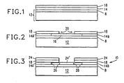
- a semiconductor device 10 ( Figure 3) is formed by a method embodying the present invention.
- a substrate 12 for example of gallium-arsenide or silicon, is coated with a thin layer of a conductive material 14, e.g., of germanium.
- a second layer 18 is formed on the layer 14 in a region over and next adjacent to desired location for a circuit component on the substrate 12.
- the substrate 12 is normally high in electrical resistance and may contain a region which is lower in electrical resistance than the substrate 12.
- Doped region 8 is produced by ion implantation, diffusion or epitaxial growth techniques. Region 8 is formed before layer 14 is placed on substrate 12.
- Doped region 8 is typically formed with either silicon, selenium, sulfur, tellurium or tin.
- the location of the circuit means is defined by producing an opening 20 in layer 18 extending over the region and formed by standard lithographic procedures for semiconductive device purposes.
- the layer 18 may be a photoresist layer which may be subsequently removed or it may be of a material such as gold, tin, molybdenum, tungsten, or palladium.
- the structure is placed in an ambient with which the exposed part of the layer 14 reacts and is thereby chemically converted below the opening 20 and in directions extending outwardly from the opening 20 to a compound 16 that is removable from the device by a reagent that will remove the compound 16 at a faster rate then the layer 14 or the layer 18 by which it is meant that the reagent will have substantially minimal to no effect on the layers 14 and 18 as well as the device 10 and substrate 12.
- the layer 14 comprises germanium and the ambient in which the device is placed comprises an oxidizing medium such as air or oxygen for the conversion of the layer 14 beneath opening 20 into a portion 16 of germanium oxide.
- the conductor 14 is then divided into two regions 14A and 14B.
- exposure of the layer 14 through the opening 20 to air and/ or other oxygen sources can be effected by the pressure or the partial pressure of the oxidizing ambient, by placement of the device in an autoclave or other pressure device or by mixing the ambient with other nonreactive compounds, such as in the case of an oxidizing gas, e.g., oxygen mixed with nitrogen or a rare gas to control the partial pressure of the oxygen.
- an oxidizing gas e.g., oxygen mixed with nitrogen or a rare gas to control the partial pressure of the oxygen.
- Compounds consisting of oxides result from oxygen-bearing ambients, while compounds consisting of nitrides result from, say, ammonia-containing ambients with active nitrogen content.
- the temperature of the ambient can also be adjusted to change the reactivity thereof.
- the rate of reaction will increase and by reducing the temperature and/or pressure of the ambient the rate of reaction will decrease.
- the partial pressures may vary from anywhere from about 0.1 atmospheres to slightly less than 1 atmosphere pressure, the pressure range for the ambient, including the partial pressure ranges being anywhere from about 0.1 atmospheres to about 1,000 atomospheres.
- the ambient may also be ionized by methods well known in the art which increases the reaction rate and allows the reaction to proceed at lower temperatures.
- the time period over which the layer 14 is exposed to the ambient through the opening 20 is also a factor that will control the extent of the development of the layer 14 into a compound 16 underneath the layer 18.
- the degree of formation of compound 16 also increases. All of these are parameters that can be adjusted by a person having ordinary skill in the art. In any event, it is critical that the compound 16 is formed to some degree underneath the layer 18 so that subsequent removal of the compound 16 by the reagent will result in some undercutting of the layer 18. Once the compound 16 is formed, to the degree and the extent determined for the production of a self-aligned semi-conductor or other device, the compound 16 is removed.
- the compound 16 may consist of germanium oxide which may be removed from the substrate 12 through opening 20 by means of a reagent such as water, hydrogen peroxide, hydrochloric acid or by plasma etching techniques.
- the plasma employed for removal of the compound 16 may comprise a plasma of a haloflouro lower alkane where the halogen compound in addition to flourine preferably comprises chlorine such as, for example carbon tetra- flouride, monochlorotriflouromethane, di- chlorodiflouromethane, and trichloromonofluoromethane.
- the substrate 12 may be converted to a semi-conductor device by deposition of a conducting material 24 through opening 20 by a conventional process.
- Layers 24 and 24' are of the same material and are deposited simultaneously and may comprise, for example tungsten or aluminum, or suitable mixtures such as tungsten - silicon or tungsten-aluminum which is placed on the semi-conductor device 10 by a known method, for example by vapor deposition.
- ohmic contact between the layer 14 and the region 8 can be formed such as in the case where layer 14A and 14B comprise germanium and the substrate 12 and region 8 comprise gallium arsenide.
- a FET is formed in which, after a lead is attached to the element 24' it can serve as a gate whereas the conductor 14A will serve as a source electrode and the conductor 14B will serve as a drain electrode.
- the distances 26 and 28 between elements 14A and 24 and elements 14B and 24 can be controlled within several hundred nanometers thereby reducing the source resistance between elements 14A and 24' and the drain resistance between elements 14B and 24 to a degree not heretofore readily achieved by known methods.
- a self-aligned structure in which semi-conductor devices can be fabricated and the components of the device can be positioned closer to one another by a method whereby the distances between components are more readily and easily controlled than previously possible.
- the element 24' may comprise any circuit component for controlling power through the device 10.
- element 24' may comprise another circuit component such as a conductor, a capacitor, a resistor or a seimcon- ductor circuit per se.
- the layer 14 may comprise a titanium or a tantalum layer and the layer 18 may comprise tin, gold, palladium or silver.
- a portion 16 of the titanium or tantalum will be converted to a compound such as titanium dioxide or tantalum oxide by anodization or oxidation through the opening 20 in the tin, palladium, gold or silver layer after which the oxide may be removed by hydrogen flouride.
Landscapes
- Physics & Mathematics (AREA)
- Engineering & Computer Science (AREA)
- Microelectronics & Electronic Packaging (AREA)
- General Physics & Mathematics (AREA)
- Optics & Photonics (AREA)
- Junction Field-Effect Transistors (AREA)
- Semiconductor Lasers (AREA)
- Electrodes Of Semiconductors (AREA)
- Drying Of Semiconductors (AREA)
Claims (7)
Applications Claiming Priority (2)
| Application Number | Priority Date | Filing Date | Title |
|---|---|---|---|
| US63597584A | 1984-07-30 | 1984-07-30 | |
| US635975 | 1984-07-30 |
Publications (3)
| Publication Number | Publication Date |
|---|---|
| EP0171226A2 EP0171226A2 (fr) | 1986-02-12 |
| EP0171226A3 EP0171226A3 (en) | 1987-08-26 |
| EP0171226B1 true EP0171226B1 (fr) | 1989-07-19 |
Family
ID=24549878
Family Applications (1)
| Application Number | Title | Priority Date | Filing Date |
|---|---|---|---|
| EP85305242A Expired EP0171226B1 (fr) | 1984-07-30 | 1985-07-23 | Procédé de fabrication d'un composant pour un circuit microélectronique et dispositif semiconducteur et guide d'ondes optiques fabriquées par ce procédé |
Country Status (3)
| Country | Link |
|---|---|
| EP (1) | EP0171226B1 (fr) |
| JP (1) | JPS6142140A (fr) |
| DE (1) | DE3571721D1 (fr) |
Families Citing this family (2)
| Publication number | Priority date | Publication date | Assignee | Title |
|---|---|---|---|---|
| JPH081897B2 (ja) * | 1987-03-27 | 1996-01-10 | 富士通株式会社 | サイドエツチング方法 |
| DE4006863A1 (de) * | 1990-03-05 | 1991-09-12 | Standard Elektrik Lorenz Ag | Optisches wellenleiterbauelement und verfahren zum herstellen eines optischen wellenleiterbauelementes |
Family Cites Families (7)
| Publication number | Priority date | Publication date | Assignee | Title |
|---|---|---|---|---|
| FR2077476A1 (fr) * | 1970-01-07 | 1971-10-29 | Semi Conducteurs | |
| US3775262A (en) * | 1972-02-09 | 1973-11-27 | Ncr | Method of making insulated gate field effect transistor |
| US3866310A (en) * | 1973-09-07 | 1975-02-18 | Westinghouse Electric Corp | Method for making the self-aligned gate contact of a semiconductor device |
| US3867148A (en) * | 1974-01-08 | 1975-02-18 | Westinghouse Electric Corp | Making of micro-miniature electronic components by selective oxidation |
| JPS5269266A (en) * | 1975-12-08 | 1977-06-08 | Fujitsu Ltd | Production of semiconductor device |
| JPS5380167A (en) * | 1976-12-24 | 1978-07-15 | Mitsubishi Electric Corp | Manufacture of semiconductor device |
| US4496419A (en) * | 1983-02-28 | 1985-01-29 | Cornell Research Foundation, Inc. | Fine line patterning method for submicron devices |
-
1985
- 1985-04-10 JP JP7455585A patent/JPS6142140A/ja active Granted
- 1985-07-23 DE DE8585305242T patent/DE3571721D1/de not_active Expired
- 1985-07-23 EP EP85305242A patent/EP0171226B1/fr not_active Expired
Also Published As
| Publication number | Publication date |
|---|---|
| EP0171226A2 (fr) | 1986-02-12 |
| DE3571721D1 (en) | 1989-08-24 |
| JPH0466099B2 (fr) | 1992-10-22 |
| JPS6142140A (ja) | 1986-02-28 |
| EP0171226A3 (en) | 1987-08-26 |
Similar Documents
| Publication | Publication Date | Title |
|---|---|---|
| US4253888A (en) | Pretreatment of photoresist masking layers resulting in higher temperature device processing | |
| US4745082A (en) | Method of making a self-aligned MESFET using a substitutional gate with side walls | |
| CA1085969A (fr) | Dispositif a semiconducteur et mode de fabrication | |
| EP0046371B1 (fr) | Procédé pour la fabrication de dispositifs à semiconducteurs | |
| US4997778A (en) | Process for forming a self-aligned FET having a T-shaped gate structure | |
| US4136434A (en) | Fabrication of small contact openings in large-scale-integrated devices | |
| US5112763A (en) | Process for forming a Schottky barrier gate | |
| US4551907A (en) | Process for fabricating a semiconductor device | |
| US4497108A (en) | Method for manufacturing semiconductor device by controlling thickness of insulating film at peripheral portion of element formation region | |
| EP0050973B1 (fr) | Procédé de masquage pour dispositif semiconducteurs utilisant une couche de polymère | |
| US4766093A (en) | Chemically formed self-aligned structure and wave guide | |
| US5114871A (en) | Manufacturing diamond electronic devices | |
| EP0171226B1 (fr) | Procédé de fabrication d'un composant pour un circuit microélectronique et dispositif semiconducteur et guide d'ondes optiques fabriquées par ce procédé | |
| KR100253394B1 (ko) | 듀얼 게이트절연막을 가지는 게이트전극의 제조방법 | |
| EP0392120B1 (fr) | Dispositif semi-conducteur utilisant des parois asymétriques accolées à la porte et méthode pour sa production | |
| US4631113A (en) | Method for manufacturing a narrow line of photosensitive material | |
| JPH11274468A (ja) | オーミック電極およびその形成方法ならびにオーミック電極形成用積層体 | |
| EP0293979A2 (fr) | Structure d'oxyde isolant sans bird-beak pour circuits intégrés | |
| US4821094A (en) | Gate alignment procedure in fabricating semiconductor devices | |
| EP0155311B1 (fr) | Procede de reparation de contacts noyes dans des dispositifs mosfet | |
| US4621415A (en) | Method for manufacturing low resistance sub-micron gate Schottky barrier devices | |
| US5021363A (en) | Method of selectively producing conductive members on a semiconductor surface | |
| EP0366939A2 (fr) | Procédé pour former une porte à barrière Schottky sur GaAs | |
| KR100281270B1 (ko) | 반도체소자의 콘택 제조방법 | |
| JPH065562A (ja) | 半導体薄膜の形成方法 |
Legal Events
| Date | Code | Title | Description |
|---|---|---|---|
| PUAI | Public reference made under article 153(3) epc to a published international application that has entered the european phase |
Free format text: ORIGINAL CODE: 0009012 |
|
| AK | Designated contracting states |
Designated state(s): DE FR GB |
|
| 17P | Request for examination filed |
Effective date: 19860523 |
|
| PUAL | Search report despatched |
Free format text: ORIGINAL CODE: 0009013 |
|
| AK | Designated contracting states |
Kind code of ref document: A3 Designated state(s): DE FR GB |
|
| 17Q | First examination report despatched |
Effective date: 19880314 |
|
| GRAA | (expected) grant |
Free format text: ORIGINAL CODE: 0009210 |
|
| AK | Designated contracting states |
Kind code of ref document: B1 Designated state(s): DE FR GB |
|
| REF | Corresponds to: |
Ref document number: 3571721 Country of ref document: DE Date of ref document: 19890824 |
|
| ET | Fr: translation filed | ||
| PLBE | No opposition filed within time limit |
Free format text: ORIGINAL CODE: 0009261 |
|
| STAA | Information on the status of an ep patent application or granted ep patent |
Free format text: STATUS: NO OPPOSITION FILED WITHIN TIME LIMIT |
|
| 26N | No opposition filed | ||
| PGFP | Annual fee paid to national office [announced via postgrant information from national office to epo] |
Ref country code: FR Payment date: 19920630 Year of fee payment: 8 |
|
| PGFP | Annual fee paid to national office [announced via postgrant information from national office to epo] |
Ref country code: DE Payment date: 19920729 Year of fee payment: 8 |
|
| PGFP | Annual fee paid to national office [announced via postgrant information from national office to epo] |
Ref country code: GB Payment date: 19930622 Year of fee payment: 9 |
|
| PG25 | Lapsed in a contracting state [announced via postgrant information from national office to epo] |
Ref country code: FR Effective date: 19940331 |
|
| PG25 | Lapsed in a contracting state [announced via postgrant information from national office to epo] |
Ref country code: DE Effective date: 19940401 |
|
| REG | Reference to a national code |
Ref country code: FR Ref legal event code: ST |
|
| PG25 | Lapsed in a contracting state [announced via postgrant information from national office to epo] |
Ref country code: GB Effective date: 19940723 |
|
| GBPC | Gb: european patent ceased through non-payment of renewal fee |
Effective date: 19940723 |