EP0046371B1 - Procédé pour la fabrication de dispositifs à semiconducteurs - Google Patents
Procédé pour la fabrication de dispositifs à semiconducteurs Download PDFInfo
- Publication number
- EP0046371B1 EP0046371B1 EP81303681A EP81303681A EP0046371B1 EP 0046371 B1 EP0046371 B1 EP 0046371B1 EP 81303681 A EP81303681 A EP 81303681A EP 81303681 A EP81303681 A EP 81303681A EP 0046371 B1 EP0046371 B1 EP 0046371B1
- Authority
- EP
- European Patent Office
- Prior art keywords
- region
- film
- wiring
- substrate
- silicon
- Prior art date
- Legal status (The legal status is an assumption and is not a legal conclusion. Google has not performed a legal analysis and makes no representation as to the accuracy of the status listed.)
- Expired
Links
Images


Classifications
-
- H—ELECTRICITY
- H10—SEMICONDUCTOR DEVICES; ELECTRIC SOLID-STATE DEVICES NOT OTHERWISE PROVIDED FOR
- H10P—GENERIC PROCESSES OR APPARATUS FOR THE MANUFACTURE OR TREATMENT OF DEVICES COVERED BY CLASS H10
- H10P14/00—Formation of materials, e.g. in the shape of layers or pillars
- H10P14/40—Formation of materials, e.g. in the shape of layers or pillars of conductive or resistive materials
- H10P14/416—Formation of materials, e.g. in the shape of layers or pillars of conductive or resistive materials of highly doped semiconductor materials, e.g. polysilicon layers or amorphous silicon layers
-
- H—ELECTRICITY
- H10—SEMICONDUCTOR DEVICES; ELECTRIC SOLID-STATE DEVICES NOT OTHERWISE PROVIDED FOR
- H10W—GENERIC PACKAGES, INTERCONNECTIONS, CONNECTORS OR OTHER CONSTRUCTIONAL DETAILS OF DEVICES COVERED BY CLASS H10
- H10W20/00—Interconnections in chips, wafers or substrates
- H10W20/01—Manufacture or treatment
- H10W20/031—Manufacture or treatment of conductive parts of the interconnections
- H10W20/064—Manufacture or treatment of conductive parts of the interconnections by modifying the conductivity of conductive parts, e.g. by alloying
- H10W20/066—Manufacture or treatment of conductive parts of the interconnections by modifying the conductivity of conductive parts, e.g. by alloying by forming silicides of refractory metals
-
- H—ELECTRICITY
- H10—SEMICONDUCTOR DEVICES; ELECTRIC SOLID-STATE DEVICES NOT OTHERWISE PROVIDED FOR
- H10W—GENERIC PACKAGES, INTERCONNECTIONS, CONNECTORS OR OTHER CONSTRUCTIONAL DETAILS OF DEVICES COVERED BY CLASS H10
- H10W20/00—Interconnections in chips, wafers or substrates
- H10W20/40—Interconnections external to wafers or substrates, e.g. back-end-of-line [BEOL] metallisations or vias connecting to gate electrodes
-
- Y—GENERAL TAGGING OF NEW TECHNOLOGICAL DEVELOPMENTS; GENERAL TAGGING OF CROSS-SECTIONAL TECHNOLOGIES SPANNING OVER SEVERAL SECTIONS OF THE IPC; TECHNICAL SUBJECTS COVERED BY FORMER USPC CROSS-REFERENCE ART COLLECTIONS [XRACs] AND DIGESTS
- Y10—TECHNICAL SUBJECTS COVERED BY FORMER USPC
- Y10S—TECHNICAL SUBJECTS COVERED BY FORMER USPC CROSS-REFERENCE ART COLLECTIONS [XRACs] AND DIGESTS
- Y10S148/00—Metal treatment
- Y10S148/15—Silicon on sapphire SOS
Definitions
- the present invention relates to a semiconductor device and a method of manufacturing a semiconductor device.
- Multi-layer wiring structures are being employed in semiconductor devices to provide for an increase in the integration density of integrated circuits.
- FIG. 1 A of the accompanying drawings which is a schematic cross-sectional view, in a known method of manufacturing a semiconductor device, there is formed a first wiring layer 2, of aluminium for example, on an insulating substrate 1.
- An insulating layer of phospho-silicate-glass (PSG) 3 is formed over the aluminium wiring layer 2, and a second wiring layer 4 of aluminium is formed on the PSG layer 3.
- PSG phospho-silicate-glass
- aluminium wiring layers 2 and 4 have a resistance of a low value.
- the wiring layer 2 has steps 2', and because of these steps, both the PSG layer 3 and the second wiring layer 4 tend also to be formed with steps 3' and 4' respectively, as shown. In such a case, the second wiring layer 4 is liable to be broken at steps 4'.
- the wiring arrangement of Figure 1A has a weakness in that manufacturing yield cannot easily be improved, although the value of resistance of aluminium is low.
- Figure 2A of the accompanying drawings is a schematic cross-sectional view, in which aluminium wiring layer 2 is replaced by a silicon wiring layer 2a.
- annealing at 1050°C is carried out for reflowing the PSG as shown in Figure 2A.
- Aluminium wiring layer 4 is then formed on the smooth PSG layer 3. This can avoid breakage of the wiring layer 4 as experienced in the arrangement of Figure 1A.
- the wiring arrangement of Figure 2A can result in an improved manufacturing yield.
- the value of resistance of silicon wiring layer 2a is high compared to that of aluminium wiring layer 2 of Figure 1A.
- single-crystal silicon is preferable to polycrystalline silicon as wiring material, because the value of resistance of single-crystal silicon is half that of polycrystalline silicon. Further, when single-crystal silicon is turned into a metal silicide, the value of its resistance is reduced by one order of magnitude. Formation of silicide wiring can be effected simultaneously with the manufacture of other parts of a semiconductor device without the need for a separate and independent process.
- the method is understood to comprise the following steps; masking, with a first mask, a thick insulating layer on a silicon substrate for fabrication of a gate, a source and a drain; to be followed by etching; covering the entire surface of the substrate with a thin layer of insulating material and a layer of polycrystalline silicon, successively; masking, with a second mask, the composite layer structure of polycrystalline silicon and insulating material for removing a part of the composite layer structure in a region where the source and drain are to be formed, to be followed by etching; introducing impurity material into the exposed region where the source and drain are to be formed; covering the entire exposed surface with a layer of metal for forming a silicide; forming a silicide on the polycrystalline silicon layer in the gate region, to form the gate; and forming a si
- Figure 3 of the accompanying drawings is a schematic cross-sectional view illustrating a structure fabricated by such a method, in which 11 is a substrate of one conductivity type, 12 indicates oxidised layers, 14 and 16 are regions doped with impurity material, 15 is a gate electrode, 17 and 18 are interconnection layers, and 19 is a metal layer.
- annealing of the structure as shown in Figure 3 is effected, and parts of the metal layer 19 in contact with silicon are turned into a silicide in a self-alignment fashion, and no reaction is noted in parts of the metal layer 19 not in contact with silicon.
- silicide formation is at or near the area over the polycrystalline silicon electrodes 15, 17 and 18 and in a surface area where the metal layer 19 is in contact with the region 14 in the substrate 11.
- the formed silicide will penetrate through the region 14. If this happens, there will be a conductive path between the metal layer 19 and the substrate 11.
- annealing for silicide formation must be terminated at an appropriate time in this method. This means that it is difficult to regulate the extent or length of annealing in the method described above. Moreover, the method cannot be repeated with certainty and resistivity cannot be reduced sufficiently.
- IBM Technical Disclosure Bulletin, Volume 17, No. 6, November 1974, pages 1831 to 1833 discloses a method of manufacturing a semiconductor device involving the conversion of polysilicon to silicide-polysilicon so as to reduce the resistance of polysilicon conductor lines on an insulating substrate.
- Hafnium silicide is suggested for such use.
- Other silicides are mentioned as possibly practical.
- a method of manufacturing a semiconductor device comprising the steps of:
- An embodiment of this invention can provide a method of manufacturing a semiconductor device provided with electrodes and wiring of a low value of resistance.
- the inventors of the present invention have taken regard of the fact that both single-crystal and polycrystalline silicon wiring can be completely turned into silicides, resulting in the provision of wiring of low resistance if they are on insulating substrates.
- silicide formation for polycrystalline silicon wiring, as well as for single-crystal wiring the operational speed of a device can be improved in addition to integration density.
- silicon wiring such as that shown at 2a, and electrodes such as that shown at 2c, in Figures 2A and 2B, are turned into silicides such as MoSi 2 or PtSi to obtain a low value of resistance, which low value is somewhere between the values of resistance of aluminium and silicon.
- a silicon layer is formed on an insulating layer of sapphire or spinel that has been deposited on a semiconductor substrate.
- An embodiment of the present invention provides a method, including the steps of: exposing a part of a single-crystal or polycrystalline silicon layer formed on an insulating substrate, depositing a film of metal over the silicon layer and annealing to form silicide of the metal, for the purpose of reducing the resistance of the single-crystal or polycrystalline silicon layer which is used as interconnection wiring or electrodes.
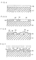
- a layer 32 of single-crystal silicon is epitaxially grown, to a thickness of approximately 0.6 pm on the surface of a single-crystal insulating substrate 31, of sapphire for example.
- insulating films 33 are formed as formed as shown in Figure 5 by a known thermal process of local oxidisation of silicon (LOCOS) using a mask of silicon nitride, for example.
- LOCOS local oxidisation of silicon
- an insulating film 34 is next formed, by a conventional thermal oxidation process.
- the film 34 may be used as a gate insulating film of a transistor to be fabricated subsequently.
- a polycrystalline silicon film is grown to a thickness of approximately 800 nm (8000 A). This film is then patterned in accordance with a known photolithography process to form a silicon gate electrode 35 and wiring 36.
- CVD chemical vapour deposition
- n-type impurity material such as arsenic (As+) is introduced by a known blanket ion implantation process, at an energy of 150 KeV, and a dosage of 5 X J0 15 CM - 2 , to form an n +- type source region 37 and an n +- type drain region 38.
- An n +- type region 39 is used for wiring purposes.
- the gate electrode 35 and the wiring 36 are also simultaneously doped with n +- type impurity material.
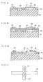
- the insulation film 34 is patterned to expose the surface of the wiring region 39 as shown in Figure 8.
- a molybdenum (Mo) film 40 is grown to a thickness of approximately 1000 nm (10000 A), as shown in Figure 9.
- metals such as titanium, platinum, nickel, magnesium, iron, hafnium, rubidium, vanadium and the like may be used singly or together.
- annealing is carried out in a nitrogen atmosphere at approximately 600°C to turn the silicon gate electrode 35, wiring 36, and wiring region 39 into Mo silicide.
- annealing is carried out in a nitrogen atmosphere at approximately 600°C to turn the silicon gate electrode 35, wiring 36, and wiring region 39 into Mo silicide.
- the substrate 31 is made of an insulating material.
- a film of silicon dioxide under the electrode 35 and under wiring 36.
- annealing can be carried out for a sufficiently long time to form silicide throughout the entire thickness of silicon films 35, 36 and 39, resulting in a lower value of resistance therefor. This is an improvement not disclosed in the unexamined Japanese Patent Publication No. 135 583 of 1978, mentioned previously.
- Mo film 40 may be removed by a known chemical etching process, utilising the difference in etching rates of Mo and MoSi 2 in which case dilute nitric or sulphuric acid may be used. Platinum, if used instead of Mo, may be removed by aqua regia.
- Wiring 36 and the wiring region 39 may cross each other as shown by the plan view of Figure 11.
- silicon dioxide film 34 on the wiring region 39, at the region at which wiring 36 and region 39 cross, is not removed and remains in position as shown by hatching in Figure 11. This means that the region 39 under the silicon dioxide 34 and the wiring 36 will not be turned into silicide and will remain as single-crystal silicon having a higher value of resistance than that of the silicide.
- the width of the wiring 36 is usually only of the order of 4 to 5 ⁇ m, whereas the length of wiring 39 is of the order of millimeters, although the value of resistance of that portion of wiring 39 at such a crossing place is not reduced, due to the large dimensional difference just mentioned, the effect of the absence of formation of silicide at the crossing portion of the wiring 36 and region 39 is negligible, and the device as a whole is very little affected thereby.
- the layer 32 of single-crystal silicon, for formation of active elements such as MOS FET's is epitaxially grown on a sapphire substrate 31.
- a silicon substrate having a film of silicon dioxide, approximately 6000 A thick, grown thereon may be used as insulating substrate 31.
- a film of single-crystal silicon approximately 5000 A thick may be formed on the film of silicon dioxide for formation of the active elements.
- a film of polycrystalline silicon, 500 nm (5000 A) thick, deposited on the film of silicon dioxide, may be turned into single-crystal silicon film by a known regrowth process using laser annealing, electron beam annealing or the like.
- a film of sapphire or spinel, 600 nm (6000 A) thick may be grown epitaxially on a single-crystal silicon substrate.
- silicon film 500 nm (5000 A thick) may be epitaxially grown on the sapphire film for formation of active regions.
- the sheet resistance of a heavily doped single-crystal silicon film 500 nm (5000 A) thick is about 20Q/square.
- the sheet resistance thereof is about 3S2/square.
- an electrode or wiring usually formed of silicon is partly exposed in accordance with a method embodying the present invention, and a film of metal capable of forming silicide when alloyed with silicon is formed on the electrode or wiring. Then annealing is carried out.
- the silicon electrode or wiring is turned into a silicide electrode or wiring, for example an electrode or wiring of MoSi 2l of which the resistance is reduced considerably.
Landscapes
- Internal Circuitry In Semiconductor Integrated Circuit Devices (AREA)
- Electrodes Of Semiconductors (AREA)
Claims (8)
Applications Claiming Priority (2)
| Application Number | Priority Date | Filing Date | Title |
|---|---|---|---|
| JP111334/80 | 1980-08-13 | ||
| JP55111334A JPS5748246A (en) | 1980-08-13 | 1980-08-13 | Manufacture of semiconductor device |
Publications (2)
| Publication Number | Publication Date |
|---|---|
| EP0046371A1 EP0046371A1 (fr) | 1982-02-24 |
| EP0046371B1 true EP0046371B1 (fr) | 1984-11-14 |
Family
ID=14558562
Family Applications (1)
| Application Number | Title | Priority Date | Filing Date |
|---|---|---|---|
| EP81303681A Expired EP0046371B1 (fr) | 1980-08-13 | 1981-08-13 | Procédé pour la fabrication de dispositifs à semiconducteurs |
Country Status (4)
| Country | Link |
|---|---|
| US (1) | US4425700A (fr) |
| EP (1) | EP0046371B1 (fr) |
| JP (1) | JPS5748246A (fr) |
| DE (1) | DE3167203D1 (fr) |
Families Citing this family (30)
| Publication number | Priority date | Publication date | Assignee | Title |
|---|---|---|---|---|
| JPS582068A (ja) * | 1981-06-26 | 1983-01-07 | Toshiba Corp | 半導体装置およびその製造方法 |
| JPS58175846A (ja) * | 1982-04-08 | 1983-10-15 | Toshiba Corp | 半導体装置の製造方法 |
| US4498223A (en) * | 1982-04-23 | 1985-02-12 | Gte Laboratories Incorporated | Method of fabrication of monolithic integrated circuit structure |
| JPS59125640A (ja) * | 1982-12-28 | 1984-07-20 | Fujitsu Ltd | 半導体装置の製造方法 |
| GB2139420B (en) * | 1983-05-05 | 1987-04-29 | Standard Telephones Cables Ltd | Semiconductor devices |
| JPS60117613A (ja) * | 1983-11-30 | 1985-06-25 | Fujitsu Ltd | 半導体装置の製造方法 |
| GB2156579B (en) * | 1984-03-15 | 1987-05-07 | Standard Telephones Cables Ltd | Field effect transistors |
| US4641417A (en) * | 1984-06-25 | 1987-02-10 | Texas Instruments Incorporated | Process for making molybdenum gate and titanium silicide contacted MOS transistors in VLSI semiconductor devices |
| US4609568A (en) * | 1984-07-27 | 1986-09-02 | Fairchild Camera & Instrument Corporation | Self-aligned metal silicide process for integrated circuits having self-aligned polycrystalline silicon electrodes |
| US5045916A (en) * | 1985-01-22 | 1991-09-03 | Fairchild Semiconductor Corporation | Extended silicide and external contact technology |
| US5227316A (en) * | 1985-01-22 | 1993-07-13 | National Semiconductor Corporation | Method of forming self aligned extended base contact for a bipolar transistor having reduced cell size |
| US5061986A (en) * | 1985-01-22 | 1991-10-29 | National Semiconductor Corporation | Self-aligned extended base contact for a bipolar transistor having reduced cell size and improved electrical characteristics |
| US4757030A (en) * | 1985-06-20 | 1988-07-12 | Cornell Research Foundation, Inc. | Method of making group IV single crystal layers on group III-V substrates using solid phase epitaxial growth |
| JPS6252550A (ja) * | 1985-08-30 | 1987-03-07 | Mitsubishi Electric Corp | フオトマスク材料 |
| US4650696A (en) * | 1985-10-01 | 1987-03-17 | Harris Corporation | Process using tungsten for multilevel metallization |
| US4843034A (en) * | 1987-06-12 | 1989-06-27 | Massachusetts Institute Of Technology | Fabrication of interlayer conductive paths in integrated circuits |
| US4906587A (en) * | 1988-07-29 | 1990-03-06 | Texas Instruments Incorporated | Making a silicon-on-insulator transistor with selectable body node to source node connection |
| FR2636472B1 (fr) * | 1988-09-09 | 1990-11-30 | France Etat | Procede de formation autoalignee de siliciure de tungstene |
| US5066613A (en) * | 1989-07-13 | 1991-11-19 | The United States Of America As Represented By The Secretary Of The Navy | Process for making semiconductor-on-insulator device interconnects |
| JP2831745B2 (ja) * | 1989-10-31 | 1998-12-02 | 富士通株式会社 | 半導体装置及びその製造方法 |
| US5288666A (en) * | 1990-03-21 | 1994-02-22 | Ncr Corporation | Process for forming self-aligned titanium silicide by heating in an oxygen rich environment |
| JP2757927B2 (ja) * | 1990-06-28 | 1998-05-25 | インターナショナル・ビジネス・マシーンズ・コーポレイション | 半導体基板上の隔置されたシリコン領域の相互接続方法 |
| DE4029060C2 (de) * | 1990-09-13 | 1994-01-13 | Forschungszentrum Juelich Gmbh | Verfahren zur Herstellung von Bauteilen für elektronische, elektrooptische und optische Bauelemente |
| US5572040A (en) * | 1993-07-12 | 1996-11-05 | Peregrine Semiconductor Corporation | High-frequency wireless communication system on a single ultrathin silicon on sapphire chip |
| US5416043A (en) * | 1993-07-12 | 1995-05-16 | Peregrine Semiconductor Corporation | Minimum charge FET fabricated on an ultrathin silicon on sapphire wafer |
| US5930638A (en) * | 1993-07-12 | 1999-07-27 | Peregrine Semiconductor Corp. | Method of making a low parasitic resistor on ultrathin silicon on insulator |
| US5863823A (en) * | 1993-07-12 | 1999-01-26 | Peregrine Semiconductor Corporation | Self-aligned edge control in silicon on insulator |
| US5864162A (en) * | 1993-07-12 | 1999-01-26 | Peregrine Seimconductor Corporation | Apparatus and method of making a self-aligned integrated resistor load on ultrathin silicon on sapphire |
| US5973363A (en) * | 1993-07-12 | 1999-10-26 | Peregrine Semiconductor Corp. | CMOS circuitry with shortened P-channel length on ultrathin silicon on insulator |
| JPH0766424A (ja) * | 1993-08-20 | 1995-03-10 | Semiconductor Energy Lab Co Ltd | 半導体装置およびその作製方法 |
Family Cites Families (7)
| Publication number | Priority date | Publication date | Assignee | Title |
|---|---|---|---|---|
| US3749614A (en) | 1970-09-14 | 1973-07-31 | Rca Corp | Fabrication of semiconductor devices |
| US3753774A (en) | 1971-04-05 | 1973-08-21 | Rca Corp | Method for making an intermetallic contact to a semiconductor device |
| US3777364A (en) | 1972-07-31 | 1973-12-11 | Fairchild Camera Instr Co | Methods for forming metal/metal silicide semiconductor device interconnect system |
| NL7510903A (nl) | 1975-09-17 | 1977-03-21 | Philips Nv | Werkwijze voor het vervaardigen van een halfgelei- derinrichting, en inrichting vervaardigd volgens de werkwijze. |
| US4102733A (en) | 1977-04-29 | 1978-07-25 | International Business Machines Corporation | Two and three mask process for IGFET fabrication |
| US4276688A (en) | 1980-01-21 | 1981-07-07 | Rca Corporation | Method for forming buried contact complementary MOS devices |
| US4336550A (en) | 1980-03-20 | 1982-06-22 | Rca Corporation | CMOS Device with silicided sources and drains and method |
-
1980
- 1980-08-13 JP JP55111334A patent/JPS5748246A/ja active Pending
-
1981
- 1981-08-07 US US06/290,972 patent/US4425700A/en not_active Expired - Lifetime
- 1981-08-13 EP EP81303681A patent/EP0046371B1/fr not_active Expired
- 1981-08-13 DE DE8181303681T patent/DE3167203D1/de not_active Expired
Also Published As
| Publication number | Publication date |
|---|---|
| US4425700A (en) | 1984-01-17 |
| JPS5748246A (en) | 1982-03-19 |
| DE3167203D1 (en) | 1984-12-20 |
| EP0046371A1 (fr) | 1982-02-24 |
Similar Documents
| Publication | Publication Date | Title |
|---|---|---|
| US4425700A (en) | Semiconductor device and method for manufacturing the same | |
| KR900008277B1 (ko) | 전계효과 트랜지스터의 제조방법 | |
| JPH02273934A (ja) | 半導体素子およびその製造方法 | |
| US4901134A (en) | Semiconductor device and manufacturing method thereof | |
| KR930011800B1 (ko) | Mos형 반도체장치 | |
| JPH0728040B2 (ja) | 半導体装置およびその製造方法 | |
| JPS627165A (ja) | 半導体装置の製造方法 | |
| JPH0127589B2 (fr) | ||
| JP3196241B2 (ja) | 半導体装置の製造方法 | |
| JPH09199717A (ja) | 半導体装置の製造方法 | |
| JP3009683B2 (ja) | 半導体不揮発性記憶素子の製造方法 | |
| JPH02226727A (ja) | Ldd型mos半導体装置の製造方法 | |
| US5021363A (en) | Method of selectively producing conductive members on a semiconductor surface | |
| JPS639748B2 (fr) | ||
| JP2822382B2 (ja) | 半導体装置及びその製造方法 | |
| JPH0622247B2 (ja) | 電界効果型半導体装置 | |
| JPH09293722A (ja) | 半導体装置の製造方法 | |
| JPH0846191A (ja) | 半導体装置の製造方法 | |
| JPH0219622B2 (fr) | ||
| JPH07147403A (ja) | 半導体装置およびその製造方法 | |
| JPH06252411A (ja) | 半導体記憶装置の製造方法 | |
| JPH01100971A (ja) | 半導体装置の製造方法 | |
| JPH0475346A (ja) | 半導体装置の製造方法 | |
| JPS61150277A (ja) | 半導体装置の製造方法 | |
| JPH08125131A (ja) | 半導体装置の製造方法 |
Legal Events
| Date | Code | Title | Description |
|---|---|---|---|
| PUAI | Public reference made under article 153(3) epc to a published international application that has entered the european phase |
Free format text: ORIGINAL CODE: 0009012 |
|
| AK | Designated contracting states |
Designated state(s): DE FR GB NL |
|
| RBV | Designated contracting states (corrected) |
Designated state(s): DE FR GB NL |
|
| 17P | Request for examination filed |
Effective date: 19820505 |
|
| GRAA | (expected) grant |
Free format text: ORIGINAL CODE: 0009210 |
|
| AK | Designated contracting states |
Designated state(s): DE FR GB NL |
|
| REF | Corresponds to: |
Ref document number: 3167203 Country of ref document: DE Date of ref document: 19841220 |
|
| ET | Fr: translation filed | ||
| PLBE | No opposition filed within time limit |
Free format text: ORIGINAL CODE: 0009261 |
|
| STAA | Information on the status of an ep patent application or granted ep patent |
Free format text: STATUS: NO OPPOSITION FILED WITHIN TIME LIMIT |
|
| 26N | No opposition filed | ||
| PGFP | Annual fee paid to national office [announced via postgrant information from national office to epo] |
Ref country code: NL Payment date: 19920831 Year of fee payment: 12 |
|
| PGFP | Annual fee paid to national office [announced via postgrant information from national office to epo] |
Ref country code: DE Payment date: 19931030 Year of fee payment: 13 |
|
| PG25 | Lapsed in a contracting state [announced via postgrant information from national office to epo] |
Ref country code: NL Effective date: 19940301 |
|
| NLV4 | Nl: lapsed or anulled due to non-payment of the annual fee | ||
| PG25 | Lapsed in a contracting state [announced via postgrant information from national office to epo] |
Ref country code: DE Effective date: 19950503 |
|
| PGFP | Annual fee paid to national office [announced via postgrant information from national office to epo] |
Ref country code: FR Payment date: 19990810 Year of fee payment: 19 |
|
| PGFP | Annual fee paid to national office [announced via postgrant information from national office to epo] |
Ref country code: GB Payment date: 19990811 Year of fee payment: 19 |
|
| PG25 | Lapsed in a contracting state [announced via postgrant information from national office to epo] |
Ref country code: GB Free format text: LAPSE BECAUSE OF NON-PAYMENT OF DUE FEES Effective date: 20000813 |
|
| GBPC | Gb: european patent ceased through non-payment of renewal fee |
Effective date: 20000813 |
|
| PG25 | Lapsed in a contracting state [announced via postgrant information from national office to epo] |
Ref country code: FR Free format text: LAPSE BECAUSE OF NON-PAYMENT OF DUE FEES Effective date: 20010430 |
|
| REG | Reference to a national code |
Ref country code: FR Ref legal event code: ST |