EP0171597B1 - Structure à pompage de charges - Google Patents
Structure à pompage de charges Download PDFInfo
- Publication number
- EP0171597B1 EP0171597B1 EP85108489A EP85108489A EP0171597B1 EP 0171597 B1 EP0171597 B1 EP 0171597B1 EP 85108489 A EP85108489 A EP 85108489A EP 85108489 A EP85108489 A EP 85108489A EP 0171597 B1 EP0171597 B1 EP 0171597B1
- Authority
- EP
- European Patent Office
- Prior art keywords
- substrate
- diode
- region
- conductivity
- epitaxial layer
- Prior art date
- Legal status (The legal status is an assumption and is not a legal conclusion. Google has not performed a legal analysis and makes no representation as to the accuracy of the status listed.)
- Expired
Links
- 238000005086 pumping Methods 0.000 title claims description 40
- 239000000758 substrate Substances 0.000 claims description 105
- 239000003990 capacitor Substances 0.000 claims description 15
- 239000002800 charge carrier Substances 0.000 claims description 13
- 230000005684 electric field Effects 0.000 claims description 8
- 230000000737 periodic effect Effects 0.000 claims description 5
- 239000000463 material Substances 0.000 claims description 4
- 230000015572 biosynthetic process Effects 0.000 claims description 3
- 230000008878 coupling Effects 0.000 claims description 3
- 238000010168 coupling process Methods 0.000 claims description 3
- 238000005859 coupling reaction Methods 0.000 claims description 3
- 230000003071 parasitic effect Effects 0.000 claims description 2
- 239000004065 semiconductor Substances 0.000 claims description 2
- 230000000903 blocking effect Effects 0.000 claims 1
- 238000002347 injection Methods 0.000 description 10
- 239000007924 injection Substances 0.000 description 10
- 238000010586 diagram Methods 0.000 description 9
- 239000000969 carrier Substances 0.000 description 8
- 230000007257 malfunction Effects 0.000 description 2
- 230000007704 transition Effects 0.000 description 2
- 238000010276 construction Methods 0.000 description 1
Images
Classifications
-
- H—ELECTRICITY
- H10—SEMICONDUCTOR DEVICES; ELECTRIC SOLID-STATE DEVICES NOT OTHERWISE PROVIDED FOR
- H10D—INORGANIC ELECTRIC SEMICONDUCTOR DEVICES
- H10D89/00—Aspects of integrated devices not covered by groups H10D84/00 - H10D88/00
- H10D89/211—Design considerations for internal polarisation
- H10D89/213—Design considerations for internal polarisation in field-effect devices
- H10D89/215—Design considerations for internal polarisation in field-effect devices comprising arrangements for charge pumping or biasing substrates
Definitions
- the invention relates in general to substrate bias generator circuits and structures for producing an electric potential in a semiconductor substrate, and more particularly to charge pumping structures used in substrate bias generators.
- MOSFET integrated circuits perform better when their common substrate is maintained at a predetermined voltage level. This can be accomplished by connecting the substrate to an external bias source or alternatively by incorporating into the integrated circuit a substrate bias generating circuit which is capable of generating a bias on the substrate and for maintaining it within a preselected range. This latter approach to biasing the substrate of integrated circuits is preferable to the earlier use of external bias sources because it eliminates the need for additional outside power supplies and the need for additional electrical connections to the substrate.
- on-chip substrate bias generators have been proposed, such as for example, the one discussed in an article by H. Frantz et al entitled "MOSFET Substrate Bias-Voltage Generator", published in the IBM Technical Disclosure Bulletin, Vol. 11, No. 10, page 1219, in March, 1969.
- Other references discussing substrate bias generating circuits and structures include U.S. Patents 3 794 862, 4 115 794, 4 336 466, 4 378 506, and 4 403 158.
- a substrate bias generator typically uses an oscillator circuit to provide a waveform potential to a charge pumping circuit.
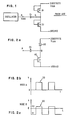
- a diagram illustrating a conventional prior art substrate bias generating circuit is shown in Fig. 1, which is described in some detail in a later section of the specification.
- the charge pumping circuit as discussed herein, is defined to include a capacitor, a first diode means that is connected between a first capacitor node and the substrate and a second diode means that is connected between the same first capacitor node and a reference potential, such as the ground.
- charge is pumped from the substrate through the first diode means to the first capacitor node in response to a negative transition of a periodic input signal coupled through the capacitor to this first node, and then from there the pumped charge passes through the second diode means to the reference potential in response to a positive going transition of a periodic input signal.
- the typical diode means used in such applications are PN junction diodes or FET type diodes.
- the substrate bias generator is used to apply a negative bias voltage to the substrate. It is therefore necessary to cause hole current to be drawn out of the substrate so as to drive the potential of the substrate to a negative level.
- the charge pumping efficiency of a charge pumping structure depends on the capacitance of the charging capacitor, the output voltage level of the oscillator which is applied on the capacitor, the pre-existing voltage level on the substrate and the threshold voltage of the diodes in the charge pumping circuit.
- the threshold voltage of the diodes used in the circuit will to a large extent determine the charge pumping efficiency of the circuit. The lower the threshold voltage level of the diodes the higher the charge pumping efficiency of the circuit.
- the diode structures be designed so that they do not inject into the substrate majority or minority carriers during any portion of the pumping cycle.
- charge pumping structures are their injection of charges into the substrate. This is undesirable regardless of the types of charge carriers injected. For example, the injections of electrons into a P-type substrate can cause the malfunction of active devices constructed in the substrate.
- holes which are the majority carriers in a P-type substrate, is undesirable because they are the very carriers which the charge pumping structure is pumping out of the substrate.
- the injection of majority carriers is counterproductive to the efficient operation of the circuit as will be further discussed during the discussion of the prior art structure shown in Fig. 1.
- EP-A 0 062 894 where the problems arising from the injection of minority carriers into the substrate are described and have been met by supply of an additional voltage, and provision of a well region of an opposite conductivity type in which the circuit elements are formed.
- a charge pumping structure having a capacitor formed on a first conductivity type substrate for coupling to a first node periodic voltage signals received at a second node.
- First diode means are provided in a first portion of the substrate for providing a current path from the first node to the substrate.
- This first portion is doped with a first type conductivity determining material having a doping concentration which is lower than the doping concentration of the first conductivity material in the adjoining first conductivity type substrate portions thereby establishing a built-in electric field in the substrate so that minority charge carriers in the first portion with the relatively lower doping concentration will be repelled by this electric field and be prevented from moving into the adjoining first conductivity portion with the relatively higher doping concentration.
- There are also means in this first substrate portion for collecting charge carriers injected into this first substrate portion by the first diode means.
- the first node is also coupled to a reference potential through a second diode means.
- the first diode means is a first PN junction diode established in the first substrate portion by the formation of a PN junction forming layer of a second conductivity type in a predetermined portion of the first conductivity type first substrate portion.
- the means for collecting minority charge carriers which are injected into the first substrate portion may include a well region of a second conductivity type around this first substrate portion.
- a first FET diode structure may be constructed having the diode forming second conductivity region as a source region and a second conductivity well contact region as a drain region.
- a gate electrode is tied to the well contact region and to a first conductivity substrate contact region.
- the charge drawn from the substrate during one portion of the oscillator cycle will have to be dissipated to a structure having a reference potential such as ground.
- This second diode means can be a second PN junction diode or a second FET diode formed in a second portion of said substrate.
- the second diode means is a pocket-type PN junction diode adopted for use in a charge pumping structure.
- Such a diode structure can reduce or eliminate the injection into the substrate of the charge carriers which during the first part of the cycle were removed from the structure and temporarily stored in the capacitor for transfer into ground through this diode during the second part of the cycle.
- charge pumping structures can be constructed with a good pumping efficiency and a minimum of undesirable charge injection into the substrate. While most discussion focuses around charge pumping structures constructed in P-type substrates for use with N-channel MOSFET circuit and the CMOS circuits built in P-type substrates, the same principles apply to the construction of charge pumping structures in either P or N type substrates.
- a prior art electrical schematic diagram of a substrate bias generator includes an oscillator applying periodic voltage signals to a charge pumping circuit.
- the charge pumping circuit includes a capacitor C1, and two N-channel FET diodes D1 and D2 connecting one side of the capacitor to the substrate and the ground respectively.
- a certain amount of charge is removed from the substrate and returned to ground. This charge per cycle is given by:
- threshold voltage refers to the amount of voltage that is required for the diode to turn-on. Thus, the lower the threshold voltage of the diodes selected, the more charge will be transferred out of the substrate during each oscillator voltage cycle.
- N-channel FET diodes inject electrons into the P type substrates.
- the injection of electrons into a P substrate can interfere with the operation of adjacent sensitive N-channel active devices. This is why we have invented a new and improved charge pumping structure such as that depicted in the embodiment shown in the schematic diagram of Fig. 2a. It includes a first diode means 30, such as that shown in Fig.
- a second diode means which could be a P-channel FET diode or a pocket-type PN junction diode as shown in Fig. 5.
- Fig. 2a there is shown a capacitor 20 between first node B and second node A.
- a PN junction diode structure 30 connects the cathode of the diode to first node B and the anode to the substrate.
- a P-channel FET diode 40 connects first node B to ground.
- the waveform 50 of a voltage signal applied to node A with the voltage going from 0 to VDD, which typically is set to about 5 volts. This may be the output of an oscillator.
- Fig. 1 there is shown a capacitor 20 between first node B and second node A.
- a PN junction diode structure 30 connects the cathode of the diode to first node B and the anode to the substrate.
- a P-channel FET diode 40 connects first node B to ground.
- V 2c there is shown the resulting voltage waveform 60 at node B. It is shown to go from a negative voltage Vi to a positive voltage V 2 .
- V 2 is basically the threshold voltage of P-channel FET diode 40, which may have a value of about 1 volt.
- V 1 will be equal to -(V DD - V 2 - V T30 )) where VT30 is the threshold voltage of diode structure 30, when no charge is being removed out of the substrate.
- V i will be less negative when charge is being removed from the substrate.
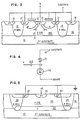
- a diode structure which includes a PN junction diode 13, for low threshold voltage, and means for preventing the minority carriers, which in this example are electrons, from reaching into adjacent active device regions and cause their malfunction. It includes a P type layer 12, which can be an epitaxial layer, formed on a P+ substrate 10.
- the substrate 10 may have a P + type doping concentration of about 1019 atoms/cm 3 while the P region 12 should have a lower doping concentration which may be in the range of 1014 to 1017 atoms/cm 3 .
- the difference in the doping concentration of layer 12 and substrate 10 causes the establishment of a built-in electric field (E) which will prevent or inhibit the movement of electrons from layer 12 to substrate 10.
- E built-in electric field
- N + region 15 forms with a first P type portion 12a of layer 12 a first PN junction diode 13.
- the N + region 15 is the cathode of the diode and is connected to node B.
- the anode 12 of this diode is connected to the substrate.
- electrons (e) are injected into P type portion 12a. Some of these electrons recombine with holes in the substrate. The remaining are deflected from going into the underlying P + substrate by the built-in electric field (E). This electric field repulses the electrons. Thus, they have to move sidewise where they are collected by the N-well region 14, which is provided by the present invention.
- Region 14 is a well region formed as a ring region around diode 13.
- Region 17 represents a contact ring region for N-well region 14, and it also forms a drain region of a first FET diode formed by N + region 15, which acts both as the N side of PN junction diode 13 and as a source of a first FET diode.
- Gate electrode 16 and drain contact region 17 are tied together. Electrons in the channel of this FET diode will move to N + region 17.
- the structure is also surrounded by a P + contact ring region 18 which, in addition to being a contact region for the epitaxial layer 12 and the underlying substrate, it is also used to interrupt any parasitic FET structures between the N-well region 14 and any other adjacent N + region.
- PN junction diode 13 can be used in the position of PN junction 30 shown in Figure 2a for the transfer majority charge carriers out of the substrate without causing the injection of minority carriers into the substrate. This is accomplished by providing device 30 as shown in Fig. 3 with the structures adjacent PN junction diode 13 for preventing the movement of such carriers into the main portions of the epitaxial layer and the substrate where active devices are located.
- FIG. 4 there is shown a schematic diagram of a charge pumping structure such as that shown in Fig. 2a, except the P-channel FET diode 40 of Fig. 2a is replaced in Fig. 4 by a special PN junction diode arrangement 140.
- An embodiment of a structure that can be used in 140 is illustrated in Fig. 5.
- Fig. 5 there is shown on the same P + type substrate 10, P type epitaxial layer 12 in which there is a PN junction diode forming a series of adjoining N-type regions consisting of N-well region 24 and buried layer 29 which, together, they define an isolated P type portion 32.
- N-type regions 24 and 29 and P-type isolated portion 32 form a second PN junction diode which is in the form of a pocket diode because of the way the N regions of this diode isolate the P-type region 32.
- An N + ring contact region 27 is provided for connecting the N side of this diode to ground, and a P + contact region 25 is provided for connecting of the P side of the diode to node B.
Landscapes
- Semiconductor Integrated Circuits (AREA)
- Metal-Oxide And Bipolar Metal-Oxide Semiconductor Integrated Circuits (AREA)
- Insulated Gate Type Field-Effect Transistor (AREA)
Claims (8)
caractérisé en ce qu'il comprend en outre une région de contact annulaire (18) de premier type de conductivité formée à l'intérieur de ladite première partie de substrat (12) et de la première région de puits adjacente (14) pour bloquer la formation de toute structure FET parasite à l'extérieur de ladite première région de puits (14) qui peut comprendre ladite première région de puits et toute autre région adjacente de deuxième conductivité.
caractérisé en ce que ladite deuxième structure de diode est une diode de type FET (140) dont la source (15) est connectée audit premier noeud (B) et dont le drain (17) et l'électrode de grille sont connectés à une source de potentiel de référence.
Applications Claiming Priority (2)
| Application Number | Priority Date | Filing Date | Title |
|---|---|---|---|
| US640421 | 1984-08-13 | ||
| US06/640,421 US4670669A (en) | 1984-08-13 | 1984-08-13 | Charge pumping structure for a substrate bias generator |
Publications (2)
| Publication Number | Publication Date |
|---|---|
| EP0171597A1 EP0171597A1 (fr) | 1986-02-19 |
| EP0171597B1 true EP0171597B1 (fr) | 1989-05-03 |
Family
ID=24568160
Family Applications (1)
| Application Number | Title | Priority Date | Filing Date |
|---|---|---|---|
| EP85108489A Expired EP0171597B1 (fr) | 1984-08-13 | 1985-07-09 | Structure à pompage de charges |
Country Status (4)
| Country | Link |
|---|---|
| US (1) | US4670669A (fr) |
| EP (1) | EP0171597B1 (fr) |
| JP (1) | JPS6149457A (fr) |
| DE (1) | DE3570016D1 (fr) |
Families Citing this family (20)
| Publication number | Priority date | Publication date | Assignee | Title |
|---|---|---|---|---|
| DE3743930A1 (de) * | 1987-12-23 | 1989-07-06 | Siemens Ag | Integrierte schaltung mit "latch-up"-schutzschaltung in komplementaerer mos-schaltungstechnik |
| ATE74453T1 (de) * | 1986-09-30 | 1992-04-15 | Siemens Ag | Integrierte schaltung in komplementaerer schaltungstechnik mit einem substratvorspannungs- generator. |
| DE8714849U1 (de) * | 1986-12-23 | 1987-12-23 | Jenoptik Jena Gmbh, Ddr 6900 Jena | Geregelter CMOS-Substratspannungsgenerator |
| IT1217104B (it) * | 1987-03-03 | 1990-03-14 | Sgs Microelettronica Spa | Circuito integrato cmos a due alimentazioni con un transistore mos integrato di protezione contro il <<latch-up>>. |
| DE3817918A1 (de) * | 1987-05-27 | 1988-12-08 | Mitsubishi Electric Corp | Halbleiterspeichereinrichtung |
| US5156989A (en) * | 1988-11-08 | 1992-10-20 | Siliconix, Incorporated | Complementary, isolated DMOS IC technology |
| US5072133A (en) * | 1989-02-16 | 1991-12-10 | The United States Of America As Represented By The Administrator Of The National Aeronautics And Space Administration | Method and apparatus for increasing resistance of bipolar buried layer integrated circuit devices to single-event upsets |
| JP2780365B2 (ja) * | 1989-08-14 | 1998-07-30 | 日本電気株式会社 | 基板電位発生回路 |
| US5148099A (en) * | 1991-04-01 | 1992-09-15 | Motorola, Inc. | Radiation hardened bandgap reference voltage generator and method |
| US5578961A (en) * | 1994-07-27 | 1996-11-26 | Motorola, Inc. | MMIC bias apparatus and method |
| US5698877A (en) * | 1995-10-31 | 1997-12-16 | Gonzalez; Fernando | Charge-pumping to increase electron collection efficiency |
| US6285052B1 (en) * | 1997-09-26 | 2001-09-04 | Advanced Micro Devices, Inc. | Integrated capacitor |
| US6166585A (en) * | 1998-08-31 | 2000-12-26 | Conexant Systems, Inc. | Methods and apparatus for a high efficiency charge pump that includes a MOSFET capacitor operating in an accumulation region |
| US6225674B1 (en) | 1999-04-02 | 2001-05-01 | Motorola, Inc. | Semiconductor structure and method of manufacture |
| JP3520973B2 (ja) * | 1999-11-30 | 2004-04-19 | Necエレクトロニクス株式会社 | 半導体装置 |
| US7138701B2 (en) * | 2003-10-02 | 2006-11-21 | International Business Machines Corporation | Electrostatic discharge protection networks for triple well semiconductor devices |
| US7791161B2 (en) * | 2005-08-25 | 2010-09-07 | Freescale Semiconductor, Inc. | Semiconductor devices employing poly-filled trenches |
| US8003478B2 (en) * | 2008-06-06 | 2011-08-23 | Semiconductor Components Industries, Llc | Method of forming a bi-directional diode and structure therefor |
| FR2960097A1 (fr) * | 2010-05-11 | 2011-11-18 | St Microelectronics Tours Sas | Composant de protection bidirectionnel |
| CN114334956B (zh) * | 2022-03-15 | 2022-06-07 | 成都市易冲半导体有限公司 | 具有耐极负电压高压引脚的交流功率开关的隔离防护结构 |
Family Cites Families (30)
| Publication number | Priority date | Publication date | Assignee | Title |
|---|---|---|---|---|
| GB1073551A (en) * | 1964-07-02 | 1967-06-28 | Westinghouse Electric Corp | Integrated circuit comprising a diode and method of making the same |
| US3878551A (en) * | 1971-11-30 | 1975-04-15 | Texas Instruments Inc | Semiconductor integrated circuits having improved electrical isolation characteristics |
| US3794862A (en) * | 1972-04-05 | 1974-02-26 | Rockwell International Corp | Substrate bias circuit |
| NL7212509A (fr) * | 1972-09-15 | 1974-03-19 | ||
| US3931634A (en) * | 1973-06-14 | 1976-01-06 | Rca Corporation | Junction-isolated monolithic integrated circuit device with means for preventing parasitic transistor action |
| US4027325A (en) * | 1975-01-30 | 1977-05-31 | Sprague Electric Company | Integrated full wave diode bridge rectifier |
| US4001869A (en) * | 1975-06-09 | 1977-01-04 | Sprague Electric Company | Mos-capacitor for integrated circuits |
| FR2325194A1 (fr) * | 1975-09-16 | 1977-04-15 | Ibm | Dispositif de pompage de charge pour semi-conducteur et son procede de fabrication |
| JPS5279787A (en) * | 1975-12-26 | 1977-07-05 | Toshiba Corp | Integrated circuit device |
| US4117507A (en) * | 1976-06-22 | 1978-09-26 | Sgs-Ates Componeti Elettronici S.P.A. | Diode formed in integrated-circuit structure |
| US4211941A (en) * | 1978-08-03 | 1980-07-08 | Rca Corporation | Integrated circuitry including low-leakage capacitance |
| US4223238A (en) * | 1978-08-17 | 1980-09-16 | Motorola, Inc. | Integrated circuit substrate charge pump |
| JPS5559756A (en) * | 1978-10-30 | 1980-05-06 | Fujitsu Ltd | Semiconductor device |
| JPS5950224B2 (ja) * | 1978-10-30 | 1984-12-07 | 富士通株式会社 | 半導体装置 |
| JPS5593252A (en) * | 1979-01-05 | 1980-07-15 | Mitsubishi Electric Corp | Substrate potential generating apparatus |
| JPS55107255A (en) * | 1979-02-12 | 1980-08-16 | Mitsubishi Electric Corp | Substrate potential generating circuit device |
| US4458158A (en) * | 1979-03-12 | 1984-07-03 | Sprague Electric Company | IC Including small signal and power devices |
| JPS6038028B2 (ja) * | 1979-07-23 | 1985-08-29 | 三菱電機株式会社 | 基板電位発生装置 |
| JPS5632758A (en) * | 1979-08-27 | 1981-04-02 | Fujitsu Ltd | Substrate bias generating circuit |
| JPS5681963A (en) * | 1979-12-08 | 1981-07-04 | Toshiba Corp | Semiconductor device |
| US4539490A (en) * | 1979-12-08 | 1985-09-03 | Tokyo Shibaura Denki Kabushiki Kaisha | Charge pump substrate bias with antiparasitic guard ring |
| JPS571252A (en) * | 1980-06-03 | 1982-01-06 | Mitsubishi Electric Corp | Semiconductor device |
| US4336466A (en) * | 1980-06-30 | 1982-06-22 | Inmos Corporation | Substrate bias generator |
| JPS5758351A (en) * | 1980-09-24 | 1982-04-08 | Toshiba Corp | Substrate biasing device |
| US4559548A (en) * | 1981-04-07 | 1985-12-17 | Tokyo Shibaura Denki Kabushiki Kaisha | CMOS Charge pump free of parasitic injection |
| US4403158A (en) * | 1981-05-15 | 1983-09-06 | Inmos Corporation | Two-way regulated substrate bias generator |
| JPS57199335A (en) * | 1981-06-02 | 1982-12-07 | Toshiba Corp | Generating circuit for substrate bias |
| JPS57204640A (en) * | 1981-06-12 | 1982-12-15 | Fujitsu Ltd | Generating circuit of substrate bias voltage |
| US4439692A (en) * | 1981-12-07 | 1984-03-27 | Signetics Corporation | Feedback-controlled substrate bias generator |
| JPH103460A (ja) * | 1996-06-19 | 1998-01-06 | Hitachi Ltd | 共用メモリの二重化システム |
-
1984
- 1984-08-13 US US06/640,421 patent/US4670669A/en not_active Expired - Fee Related
-
1985
- 1985-05-17 JP JP60104129A patent/JPS6149457A/ja active Granted
- 1985-07-09 EP EP85108489A patent/EP0171597B1/fr not_active Expired
- 1985-07-09 DE DE8585108489T patent/DE3570016D1/de not_active Expired
Non-Patent Citations (1)
| Title |
|---|
| PATENTS ABSTRACTS OF JAPAN, vol. 7, no. 72 (E-166) [1217], 25th March 1983 & JP - A - 58 2064 * |
Also Published As
| Publication number | Publication date |
|---|---|
| JPH0347587B2 (fr) | 1991-07-19 |
| US4670669A (en) | 1987-06-02 |
| EP0171597A1 (fr) | 1986-02-19 |
| DE3570016D1 (en) | 1989-06-08 |
| JPS6149457A (ja) | 1986-03-11 |
Similar Documents
| Publication | Publication Date | Title |
|---|---|---|
| EP0171597B1 (fr) | Structure à pompage de charges | |
| EP0062894B1 (fr) | Dispositif semi-conducteur | |
| US6429723B1 (en) | Integrated circuit with charge pump and method | |
| EP0143157B1 (fr) | Circuit de pompage de charge pour un générateur de tension de substrat | |
| US6750515B2 (en) | SCR devices in silicon-on-insulator CMOS process for on-chip ESD protection | |
| KR100220385B1 (ko) | 정전기 보호 소자 | |
| US4377756A (en) | Substrate bias circuit | |
| EP0277193B1 (fr) | Circuit redresseur biphase | |
| JPS62296474A (ja) | 縦形mosfet | |
| US4072868A (en) | FET inverter with isolated substrate load | |
| US5243214A (en) | Power integrated circuit with latch-up prevention | |
| EP1048076B1 (fr) | Redresseur a thyristors a tension de maintien et de declenchement faible pour la protection contre les decharges electrostatiques | |
| JPS6064471A (ja) | 高電圧絶縁ゲ−ト型電界効果トランジスタ | |
| US4672402A (en) | Semiconductor circuit device including an overvoltage protection element | |
| US4539490A (en) | Charge pump substrate bias with antiparasitic guard ring | |
| EP0184222B1 (fr) | Circuit intégré de type MOS ayant des transistors de charge et de décharge | |
| EP0195236A2 (fr) | Générateur de polarisation de substrat semi-conducteur | |
| KR0136595B1 (ko) | 상보형 mos 회로기술을 이용한 래치업 방지회로를 가진 집적회로 | |
| JP3450358B2 (ja) | 半導体装置 | |
| JP2980108B2 (ja) | 集積mosパワー・トランジスタを含むコンポーネントのロジック・ウエルの保護 | |
| JP2901621B2 (ja) | 導電変調型mosデバイス | |
| US5815026A (en) | High efficiency, high voltage, low current charge pump | |
| EP0492339B1 (fr) | Technique de réduction du bruit de fond pour diodes à claquage | |
| US4952998A (en) | Integrated circuit with complementary MOS transistors | |
| JPH0575119A (ja) | Soi型半導体装置 |
Legal Events
| Date | Code | Title | Description |
|---|---|---|---|
| PUAI | Public reference made under article 153(3) epc to a published international application that has entered the european phase |
Free format text: ORIGINAL CODE: 0009012 |
|
| AK | Designated contracting states |
Designated state(s): DE FR GB |
|
| 17P | Request for examination filed |
Effective date: 19860624 |
|
| 17Q | First examination report despatched |
Effective date: 19880308 |
|
| GRAA | (expected) grant |
Free format text: ORIGINAL CODE: 0009210 |
|
| AK | Designated contracting states |
Kind code of ref document: B1 Designated state(s): DE FR GB |
|
| REF | Corresponds to: |
Ref document number: 3570016 Country of ref document: DE Date of ref document: 19890608 |
|
| ET | Fr: translation filed | ||
| PLBE | No opposition filed within time limit |
Free format text: ORIGINAL CODE: 0009261 |
|
| STAA | Information on the status of an ep patent application or granted ep patent |
Free format text: STATUS: NO OPPOSITION FILED WITHIN TIME LIMIT |
|
| 26N | No opposition filed | ||
| PGFP | Annual fee paid to national office [announced via postgrant information from national office to epo] |
Ref country code: FR Payment date: 19920630 Year of fee payment: 8 |
|
| PGFP | Annual fee paid to national office [announced via postgrant information from national office to epo] |
Ref country code: DE Payment date: 19920729 Year of fee payment: 8 |
|
| PGFP | Annual fee paid to national office [announced via postgrant information from national office to epo] |
Ref country code: GB Payment date: 19930622 Year of fee payment: 9 |
|
| PG25 | Lapsed in a contracting state [announced via postgrant information from national office to epo] |
Ref country code: FR Effective date: 19940331 |
|
| PG25 | Lapsed in a contracting state [announced via postgrant information from national office to epo] |
Ref country code: DE Effective date: 19940401 |
|
| REG | Reference to a national code |
Ref country code: FR Ref legal event code: ST |
|
| PG25 | Lapsed in a contracting state [announced via postgrant information from national office to epo] |
Ref country code: GB Effective date: 19940709 |
|
| GBPC | Gb: european patent ceased through non-payment of renewal fee |
Effective date: 19940709 |