EP0173413A2 - Farbbildsensor - Google Patents
Farbbildsensor Download PDFInfo
- Publication number
- EP0173413A2 EP0173413A2 EP85303600A EP85303600A EP0173413A2 EP 0173413 A2 EP0173413 A2 EP 0173413A2 EP 85303600 A EP85303600 A EP 85303600A EP 85303600 A EP85303600 A EP 85303600A EP 0173413 A2 EP0173413 A2 EP 0173413A2
- Authority
- EP
- European Patent Office
- Prior art keywords
- cell arrays
- image sensor
- color
- image
- photosensitive
- Prior art date
- Legal status (The legal status is an assumption and is not a legal conclusion. Google has not performed a legal analysis and makes no representation as to the accuracy of the status listed.)
- Granted
Links
Images


Classifications
-
- H—ELECTRICITY
- H10—SEMICONDUCTOR DEVICES; ELECTRIC SOLID-STATE DEVICES NOT OTHERWISE PROVIDED FOR
- H10F—INORGANIC SEMICONDUCTOR DEVICES SENSITIVE TO INFRARED RADIATION, LIGHT, ELECTROMAGNETIC RADIATION OF SHORTER WAVELENGTH OR CORPUSCULAR RADIATION
- H10F39/00—Integrated devices, or assemblies of multiple devices, comprising at least one element covered by group H10F30/00, e.g. radiation detectors comprising photodiode arrays
- H10F39/10—Integrated devices
- H10F39/12—Image sensors
- H10F39/191—Photoconductor image sensors
- H10F39/192—Colour image sensors
-
- H—ELECTRICITY
- H04—ELECTRIC COMMUNICATION TECHNIQUE
- H04N—PICTORIAL COMMUNICATION, e.g. TELEVISION
- H04N1/00—Scanning, transmission or reproduction of documents or the like, e.g. facsimile transmission; Details thereof
- H04N1/46—Colour picture communication systems
- H04N1/48—Picture signal generators
- H04N1/486—Picture signal generators with separate detectors, each detector being used for one specific colour component
Definitions
- the present invention relates generally to a contact type image sensor, and, more particularly, to a contact type color image sensor formed using amorphous semiconductor film.
- This photoelectric converting unit is formed of a small solid-state CCD imaging device of 2048 bits and approximately 32 to 46 mm long.
- a lens is used to focus the image of the document on the photosensitive surface of this small CCO image sensor and to reduce the image size.
- a typical A4 document 200 mm wide must be reduced to 32-46 mm. In order to obtain this degree of reduction the distance from the document to the image sensor must be increased, which makes it difficult to build a compact facsimile terminal.
- the length of the sensor array is substantially the same as the width of the document, which means that image reduction before the image reaches the image sensor is not necessary.
- the length of the optical path from the document surface to the photoelectric converting unit can be decreased to around 10 mm because a real-size (1:1 magnification) optical system, such as a rod lens array is used for forming the image.
- the inventors have proposed arranging a plurality of cells for sensing the three primary colors of one pixel in the width direction of the contact type image sensor (Japanese Patent Application No. 58-220972). With this improvement in the arrangement of the cells, the color separation is carried out in the sub-scanning direction of the contact type image sensor, so it is possible to prevent a reduction in the S/N ratio. The result of this is that the color image sensor is improved to have the same S/N ratio as a monochrome sensor to which a color filter has been attached.
- the pixel electrodes of the contact type image sensor when they are arranged contiguously along the sub-scanning direction, they must be made smaller than the pixel electrodes in the main scanning direction. Consequently, the photosensitive area is reduced by,- the amount of the decrease in size of the electrodes in the sub-scanning direction. This decrease in photosensitive area brings with it (1) a lower S/N ratio and (2) great difficulty in positioning of the sensor in relation to the pixels of the color filter, making mounting on the sensor difficult.
- the contact type color image sensor of the invention reads out an image which is the actual size of the document while moving in the lengthwise direction of the document.
- This color image sensor comprises photosensitive cell arrays aligned on a substrate and each having n photosensitive cells (n being a positive integer).
- a filter section is positioned on top of the photosensitive arrays, and -receives the input image light, filters this image light and radiates the light components of the special basic colors onto the photosensitive cell arrays.
- the three primary color signals (R, G, B signals) necessary for the reproduction of the color document are output from each of the photosensitive arrays.
- the pitch of the cell arrays on the substrate is k times wider than the pitch of the n photosensitive cells in each cell array. (The value k is larger than 1 and k-n is a natural number.)
- an insulative substrate 10 is formed of a glass substrate or a ceramic substrate on the surface of which a glazed layer has been formed.
- One pixel array is formed of n pixel electrodes linearly arranged across the length which corresponds to the width of the whole document. These pixel electrodes have the same construction and are 4n in number.
- Signal read-out electrodes 14a-14d extend in the sub-scanning direction Y from the four columns of pixel electrodes 12a-12d. These read-out electrodes are 4n in number and are connected to the pixel electrodes.
- Signal read-out electrodes 14a and 14d in the sub-scanning direction Y are connected to pixel electrode arrays 12a and 12d, which are positioned on either sides of substrate 10, and extend in mutually opposite directions.
- the planar pattern of the pixel electrode of pixel electrode arrays 12a and 12d is narrower than that of the pixel electrode in arrays 12b and 12c remaining in the center of substrate 10. Consequently, the space between the two neighbouring pixel electrodes is increased.
- Signal read-out electrodes 14b and 14c, which are connected to the center pixel electrode arrays 12b and 12c, and which pass through the spaces between the pixel electrodes included in pixel electrode arrays 12a and 12d, extend in opposite directions along the secondary scanning direction.
- Material for pixel electrodes 14 may be selected from any one or more of a group composed of chromium (Cr), tantalum (Ta), tungsten (W), titanium (Ti), aluminum (Al), vanadium (V), nickel (Ni), copper (Cu), platinum (Pt), gold (Au).
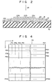
- Fig. 2 is a cross section along line II-II of the contact type image sensor of Fig. 1.
- Substrate 10, on which pixel electrodes 12 are formed has an amorphous semiconductor layer 16 deposited over the entire surface.
- amorphous semiconductor material such as silicon, silicon carbon, or silicon germanium.
- This amorphous semiconductor material is a compound or a mixture including hydrogen (H) and fluorine (F). Boron (B), phosphorous (P), nitrogen (N) or oxygen (0), etc. may be doped on layer 16 as required.
- the layer region in which layer 16 and each pixel electrode 12 contact corresponds to photoelectric converting element region P (pixel region) of the image sensor.
- a transparent, conductive layer 18 made of indium-tin-oxide (ITO) is formed on amorphous silicon layer 16 to serve as a common electrode.
- Transparent, common electrode 18 functions as a barrier layer against electrons or holes entering layer 16.
- Transparent protective layer 20 is provided on ITO layer 18. This layer, though not always necessary, is for protecting amorphous semiconductor layer 16 and common electrode 18, and is formed of an organic material such as polyparaxylylene or polyimide, or inorganic material such as silicon oxide (Si02), aluminum oxide (Al 2 O 3 ), tantalum oxide (Ta 2 0 5 ) or silicon nitrogen (SiN x ).
- Color filter films 22a, 22b, 22c are provided on protective layer 20 and respectively cover the three columns of pixel electrode arrays 12a, 12b, 12c.
- One color filter film covers n underlaying pixel electrodes.
- These filters are transparent only to the red, green and blue color components of color optical image 24, which is radiated on the image sensor, and are consequently referred to as R pass filter, G pass filter and B pass filter.
- R pass filter As a result of these filters, pixel electrode array 12a is photosensitive to red light, array 12b is photosensitive to green light, and array 12c is photosensitive to blue light.
- No filter is provided on the fourth pixel electrode array.12d so it is photosensitive to all light, i.e., white light.
- the outside pixel electrode array 12a which is smaller in area than the other pixel areas of each pixel electrode, is covered by R pass filter 22a.
- This arrangement provides a uniform output from the image sensor of the three color components because the transmission rates of the red pass filters is greater than the transmission rate of the green or blue pass filter, and this difference in transmission rates compensates for the difference in pixel area.
- the value of k.n is a natural number larger than 1.
- parameter k which determines the pixel pitch q in the sub-scanning direction Y, can be selected from the series, 1.01, 1.02,... 1.98, 1.99, 2, 2.01....
- k is taken to equal 2 so pixel pitch q in the sub-scanning direction Y is 2.p.
- the length of the pixel electrodes in the sub-scanning direction Y is equal to pitch q in this scanning direction Y so the gaps between the pixel electrodes of the two adjacent pixel electrode arrays (12a and 12b, or 12b and 12c) along the sub-scanning direction Y also have a length equal to 1 in the sub-scanning direction of the pixel electrodes.
- the length l of the gaps between the pixel electrodes of the two adjacent pixel electrode arrays (12a and 12b, or 12b and 12c) along the sub-scanning direction Y expands to become equal to any length of the pixel electrode in the secondary scanning direction.
- pixel electrode array 12a which is photosensitive to only red light, is referred to as R pixel area 30 because of the effect of R pass filter 22a, and array 12b becomes G pixel area 32 and array 12c becomes B pixel area 34 due to the effect of the respective filters 22b and 22c.
- Pixel electrode array 12d on which no filter is provided is referred to as W pixel area 36.
- Pixel electrodes 12a which are in R pixel area 30, are connected to common signal output lines 40-1, 40-2,..., 40-n by way of switches 42. Common signal output lines 40 are connected to analog/digital converter circuit 44.
- the pixel electrodes 12b included in G pixel area 32 are connected to common signal output line 46 via switches 48-1, 48-2,..., 48-n, and line 46 is connected to A/D converter circuit 50 and 2n long delay register 52.
- the pixel electrodes 12c included in B pixel area 34 are connected to common signal output line 54 via switches 56-1, 56-2,..., 56-n, and line 54 is connected to A/D converter circuit 58 and 4n long delay register 60.
- the pixel electrodes 12d included in W pixel area 36 are connected to common signal output line 62 via switches 64-1, 64-2,..., 64-n, and line 62 is connected to A/D converter circuit 6 4 and 6n long delay register 66.
- the width of document 70 to be read by the facsimile system corresponds to the total length of the contact type image sensor so it is divided into n unit image areas (or document images) along the direction X, corresponding to the number (n) of pixel electrodes included in each pixel electrode array 12 of the sensor. If the length of document 70 (corresponding to the sub-scanning direction Y) is divided into m unit image areas (m is a positive integer), the total reading area of document 70 will.be n X m unit image areas.
- switches 64 sequentially become conductive, 64-1, 64-2,..., 64-n.
- the brightness data of the unit image areas Pll, P12,..., PIn sequentially appears on common output line 62 as electric signals. These brightness signals are converted to digital signals by A/D converter 64 and stored in the first of the n stages of delay register 66.
- B pixel area 34 is positioned at a certain position corresponding to the first line of the document 70 including unit images Pll, P12, ..., PIn switches 56-1, 56-2, ..., 56-n are driven to sequentially become conductive-, resulting that blue color data of the unit images Pll, P12, ..., Pin sequentially appear on the common output line 54 as electrical blue color signals.
- B color signals are converted to digital signals by A/D converter 58 and then stored in n-th to 1st stage registers of delay register 60.
- G pixel area 32 is positioned corresponding to the aforementioned first line including unit images Pll, P12, ..., Pln, switches 48-1, 48-2, ... 48-n sequentially rendered conductive, resulting that electrical signals representing green color data of these unit images Pll, P12, ..., Pin sequentially appear on the common output line 46.
- These G color signals are converted to digital signals by A/D converter 50 and stored in n-th to 1st stage registers of delay register 52.
- Delay registers 66, 60, 52 transmit signals synchronous with the same clock signal so when the red color signal of the unit images Pll, P12,..., PIn in the first line of document 70 is sequentially output, the green, blue and brightness signals of the same unit image Pll, P12,...Pln are obtained from the three delay registers 52, 60, 66 synchronous with the output timing of the red signal.
- the read operation of the pixel areas in the other direction of the document is substantially the same as the above.
- the red, green, blue and the brightness signal obtained with respect to the whole image area of the document are compensated by the matrix circuit (not shown) if the final output signal requires it.
- the three filters 22 of Fig. 1 may be changed to transmit that particular light.
- the red, green and blue cells necessary to obtain the color image signal of the unit image or picture element P are arranged in the width direction of the image sensor, or sub-scanning direction Y so the image resolution in the main scanning direction X is substantially the same as that of a monochrome image sensor.
- the size of the pixel electrodes in the main scanning direction can be improved to be made the same as that of a monochrome image sensor.
- the size of the pixel electrodes in the sub-scanning direction is, at the maximum, equal to the length in the sub-scanning direction of the pixel to be read so the area of each pixel electrode can be increased to the maximum and the S/N ratio of the color reproduction output signal can be improved.
- the number k is carefully selected to be a specific parameter which is larger than 1 and allows the resultant product k.n to become a natural number.
- the feature that pixel pitch q becomes larger than pitch p by the multiple k is extremely important and provides the following effect.
- the signal delay occurring at the delay registers 52, 60, 66 increases in order 2n, 4n, 6n.
- pitch q is twice the size of pitch p.
- the signal delay process at the delay registers 52, 60, 66 is sequentially increased by k times. Consequently, the read-out timing misalignment of the R, G, B, W signals (these are read from cell arrays 30, 32, 34, 36, respectively) of one unit image (such as P 11 ) can be accurately compensated.
- Fig. 5 is a plan view of the main elements of the contact type color image sensor according to the second embodiment of this invention.
- the same reference numbers have been used for parts corresponding to those shown in Fig. 1, and description of which has been omitted.
- Light shield film 80 is added onto common, transparent electrode layer 18 of the color image sensor.
- This light shield film is made of electrically conductive and opaque material, such as chromium or titanium.
- Film 80 has flat openings 82a, 82b, 82c, 82d, which have the same shape as the underlying pixel electrodes 12a, 12b, 12c, 12d.
- the positional relationship of openings 82 and electrodes 12 can be readily understood from the cross section shown in Fig. 6.
- the planar shape of light shield film 80 is also illustrated in Fig. 6.
- the area of each pixel electrode of the two pixel arrays 12a and 12d on the outer sides is smaller than that of the electrodes of the center pixel arrays 12b and 12c, so openings 82a and 82d are also correspondingly smaller.
- Figs. 8 and 9 show a variation in the formation of the color filter layers (corresponding to filters 22 of Figs. 1, 2, 5 or 6) and the light shield film (80).
- two color filters 90a and 90b are formed on transparent protective layer 20 such that they partially overlap.
- the one color filter 90a is a yellow pass filter (Y-filter), and covers the top of cell arrays 12a and 12b.
- the other color filter 90b is a cyan pass filter (Cy-filter), and covers the top of cell arrays 12b and 12c.
- the document image light radiated onto cell array 12b passes through the two layers of Y-filter 90a and Cy-filter 90b converting it into green light.
- the overlapping portion of Y-filter 90a and Cy-filter 90b functions as a green pass filter (G-filter).
- G-filter green pass filter
- the Cy-filter and G-filter have a lower degree of light transmissivity than the Y-filter, so this Cy-filter and G-filter section is positioned over photosensitive cell arrays 12b and 12c, which have a larger pixel electrode area. In this way it is possible to obtain image signals that have a uniform color level for the three primary colors.
- conductive light shield film 80 which has openings 82 corresponding to the pixel electrodes, is formed on transparent protective layer 20.
- This structure is possible when the resistance of transparent electrode 18, which is shared by all the pixel electrodes, is only several hundred ohms. In this case, the liquid chemical used in the etching of the light shield film 80 during the patterning process is obstructed from progressing further by protective layer 20. Accordingly, transparent electrode 18, which is weak against this chemical is not damaged.
- a color image sensor which separates light into four colors, including white was described.
- This invention is not, however, limited to this, and may be applied to a color image sensor which divides light into three colors.
- cell arrays 22a, 22b, 22c which are respectively prescribed by the plurality of pixel electrodes arranged in the main scanning direction X, are formed on substrate 10 and, as shown in Fig. 11, R, G, B filters are arranged on top of them.
- Signal output lines 14b of pixel electrodes 12b included in the photosensing cell array in the center are alternately spaced in the main scanning direction X and extend in opposite directions in the secondary scanning direction Y. With this kind of arrangement, signal output lines 14b pass through the gap betwen pixel electrodes 12a included in the outside photosensing cell arrays, and lead to the outside. Signal output lines 14b pass through the gaps of pixel electrodes 12c included in the other outside photosensing cell array, and lead outside. In this case, the planar size of the pixel electrodes 12a and 12c included in the two cell arrays on the outside is smaller than that of the pixel electrodes 12b included in the photosensing cell array in the center by size of the gap.
Landscapes
- Engineering & Computer Science (AREA)
- Multimedia (AREA)
- Signal Processing (AREA)
- Facsimile Heads (AREA)
- Solid State Image Pick-Up Elements (AREA)
Applications Claiming Priority (2)
| Application Number | Priority Date | Filing Date | Title |
|---|---|---|---|
| JP174386/84 | 1984-08-22 | ||
| JP59174386A JPS6152061A (ja) | 1984-08-22 | 1984-08-22 | 密着型カラ−イメ−ジセンサ |
Publications (3)
| Publication Number | Publication Date |
|---|---|
| EP0173413A2 true EP0173413A2 (de) | 1986-03-05 |
| EP0173413A3 EP0173413A3 (en) | 1988-08-31 |
| EP0173413B1 EP0173413B1 (de) | 1990-07-25 |
Family
ID=15977701
Family Applications (1)
| Application Number | Title | Priority Date | Filing Date |
|---|---|---|---|
| EP85303600A Expired EP0173413B1 (de) | 1984-08-22 | 1985-05-22 | Farbbildsensor |
Country Status (4)
| Country | Link |
|---|---|
| US (1) | US4663535A (de) |
| EP (1) | EP0173413B1 (de) |
| JP (1) | JPS6152061A (de) |
| DE (1) | DE3578843D1 (de) |
Cited By (7)
| Publication number | Priority date | Publication date | Assignee | Title |
|---|---|---|---|---|
| GB2175170B (en) * | 1985-04-09 | 1989-12-20 | Canon Kk | Image reading device |
| GB2183120B (en) * | 1985-10-28 | 1990-02-21 | Hasselblad Ab Victor | Adevice to convert a presentation of a colour image to an electrical signal. |
| EP0392782A3 (de) * | 1989-04-10 | 1991-08-21 | Canon Kabushiki Kaisha | Photoelektrisches Umwandlungsgerät |
| EP0449477A1 (de) * | 1990-03-26 | 1991-10-02 | Seiko Instruments Inc. | Farbbildsensor |
| EP0363146A3 (de) * | 1988-10-04 | 1991-12-04 | Canon Kabushiki Kaisha | Farbbildverarbeitungsgerät |
| US5173759A (en) * | 1990-02-06 | 1992-12-22 | Kyocera Corporation | Array of light emitting devices or photo detectors with marker regions |
| US5721628A (en) * | 1988-10-04 | 1998-02-24 | Canon Kabushiki Kaisha | Color image processing apparatus |
Families Citing this family (30)
| Publication number | Priority date | Publication date | Assignee | Title |
|---|---|---|---|---|
| US4894700A (en) * | 1985-04-09 | 1990-01-16 | Fuji Xerox Co., Ltd. | Image sensor |
| US4803375A (en) * | 1985-12-27 | 1989-02-07 | Kabushiki Kaisha Toshiba | Image sensors and methods of manufacturing same including semiconductor layer over entire substrate surface |
| JPS62154780A (ja) * | 1985-12-27 | 1987-07-09 | Toshiba Corp | イメ−ジセンサ |
| JPH0740711B2 (ja) * | 1986-06-20 | 1995-05-01 | キヤノン株式会社 | 光センサの駆動方法及び画像入力装置 |
| JPH0612813B2 (ja) * | 1987-05-29 | 1994-02-16 | 松下電器産業株式会社 | 視覚センサ− |
| JPS6447165A (en) * | 1987-08-17 | 1989-02-21 | Fuji Xerox Co Ltd | Color image sensor |
| US5204762A (en) * | 1987-10-30 | 1993-04-20 | Canon Kabushiki Kaisha | Image reading device |
| JPH02275670A (ja) * | 1989-01-18 | 1990-11-09 | Canon Inc | 光電変換装置および画像読取装置 |
| US5075770A (en) * | 1989-03-24 | 1991-12-24 | Polaroid Corporation | Color balanced image detector system |
| JPH0354964A (ja) * | 1989-07-21 | 1991-03-08 | Ricoh Co Ltd | カラーイメージセンサ |
| DE4002429A1 (de) * | 1990-01-27 | 1991-08-01 | Philips Patentverwaltung | Sensormatrix |
| US5138416A (en) * | 1991-07-12 | 1992-08-11 | Xerox Corporation | Multi-color photosensitive element with heterojunctions |
| JPH0568132A (ja) * | 1991-09-05 | 1993-03-19 | Fuji Xerox Co Ltd | 原稿読取り装置 |
| KR940002974B1 (ko) * | 1991-11-06 | 1994-04-09 | 주식회사 금성사 | 컬러 콘택트 이미지 센서 |
| US5229595A (en) * | 1991-12-19 | 1993-07-20 | Xerox Corporation | Fluid-filled color filtered input scanner arrays |
| JP3308592B2 (ja) * | 1992-06-17 | 2002-07-29 | 株式会社東芝 | 固体撮像装置及びその信号処理方法 |
| US5424574A (en) * | 1992-09-23 | 1995-06-13 | Scientific Imaging Technologies, Inc. | Light shield for a back-side thinned CCD |
| US5483053A (en) * | 1994-09-27 | 1996-01-09 | Hewlett-Packard Company | Variable resolution color image scanner having an exposure delay between successive linear photosensors detecting different colors |
| US5519514A (en) * | 1995-05-22 | 1996-05-21 | Xerox Corporation | Color sensor array with independently controllable integration times for each color |
| JP3143053B2 (ja) * | 1995-10-31 | 2001-03-07 | キヤノン株式会社 | リニアイメージセンサ |
| DE19542241C2 (de) | 1995-11-13 | 2003-01-09 | Siemens Ag | Optoelektronisches Bauelement in II-VI-Halbleitermaterial |
| KR100209758B1 (ko) * | 1996-06-26 | 1999-07-15 | 구본준 | 고체 촬상 소자 및 그의 제조 방법 |
| US7335965B2 (en) * | 1999-08-25 | 2008-02-26 | Micron Technology, Inc. | Packaging of electronic chips with air-bridge structures |
| US7276788B1 (en) | 1999-08-25 | 2007-10-02 | Micron Technology, Inc. | Hydrophobic foamed insulators for high density circuits |
| US6890847B1 (en) * | 2000-02-22 | 2005-05-10 | Micron Technology, Inc. | Polynorbornene foam insulation for integrated circuits |
| US20040246544A1 (en) * | 2003-06-05 | 2004-12-09 | Xerox Corporation | Image sensor array with multiple exposure times |
| KR100675830B1 (ko) * | 2004-03-11 | 2007-01-29 | 주식회사 애트랩 | 이미지 센서, 광 포인팅 장치 및 광 포인팅 장치의 움직임계산 방법 |
| US9473714B2 (en) * | 2010-07-01 | 2016-10-18 | Semiconductor Energy Laboratory Co., Ltd. | Solid-state imaging device and semiconductor display device |
| JP6521586B2 (ja) * | 2014-07-31 | 2019-05-29 | キヤノン株式会社 | 固体撮像素子および撮像システム |
| JP7134911B2 (ja) * | 2019-04-22 | 2022-09-12 | キヤノン株式会社 | 固体撮像素子および撮像システム |
Family Cites Families (10)
| Publication number | Priority date | Publication date | Assignee | Title |
|---|---|---|---|---|
| JPS5941351B2 (ja) * | 1976-09-13 | 1984-10-06 | 株式会社日立製作所 | カラ−用固体撮像素子 |
| JPS56165362A (en) * | 1980-05-26 | 1981-12-18 | Hitachi Ltd | Manufacture of solid state color image pickup element |
| DE3039451A1 (de) * | 1980-10-18 | 1982-05-27 | Agfa-Gevaert Ag, 5090 Leverkusen | Vorrichtung zum elektronischen abtasten von bildern |
| DE3280262D1 (de) * | 1981-05-25 | 1990-11-29 | Toshiba Kawasaki Kk | Festkoerper-bildsensor. |
| JPS5948954A (ja) * | 1982-09-13 | 1984-03-21 | Kyocera Corp | 密着型読み取り装置 |
| US4542409A (en) * | 1983-03-25 | 1985-09-17 | Fuji Photo Film Co., Ltd. | Single gate line interlace solid-state color imager |
| US4558365A (en) * | 1983-06-06 | 1985-12-10 | Fuji Photo Film Co., Ltd. | High-resolution high-sensitivity solid-state imaging sensor |
| JPS59227157A (ja) * | 1983-06-08 | 1984-12-20 | Hitachi Ltd | ラインセンサ |
| JPS6017951A (ja) * | 1983-07-11 | 1985-01-29 | Toshiba Corp | 光電変換素子の配列構造 |
| JPS60123059A (ja) * | 1983-12-08 | 1985-07-01 | Toshiba Corp | 密着型カラ−イメ−ジセンサ |
-
1984
- 1984-08-22 JP JP59174386A patent/JPS6152061A/ja active Pending
-
1985
- 1985-05-22 EP EP85303600A patent/EP0173413B1/de not_active Expired
- 1985-05-22 DE DE8585303600T patent/DE3578843D1/de not_active Expired - Lifetime
- 1985-05-22 US US06/736,860 patent/US4663535A/en not_active Expired - Lifetime
Cited By (8)
| Publication number | Priority date | Publication date | Assignee | Title |
|---|---|---|---|---|
| GB2175170B (en) * | 1985-04-09 | 1989-12-20 | Canon Kk | Image reading device |
| GB2183120B (en) * | 1985-10-28 | 1990-02-21 | Hasselblad Ab Victor | Adevice to convert a presentation of a colour image to an electrical signal. |
| EP0363146A3 (de) * | 1988-10-04 | 1991-12-04 | Canon Kabushiki Kaisha | Farbbildverarbeitungsgerät |
| US5721628A (en) * | 1988-10-04 | 1998-02-24 | Canon Kabushiki Kaisha | Color image processing apparatus |
| EP0392782A3 (de) * | 1989-04-10 | 1991-08-21 | Canon Kabushiki Kaisha | Photoelektrisches Umwandlungsgerät |
| US5128533A (en) * | 1989-04-10 | 1992-07-07 | Canon Kabushiki Kaisha | Photoelectric converting apparatus |
| US5173759A (en) * | 1990-02-06 | 1992-12-22 | Kyocera Corporation | Array of light emitting devices or photo detectors with marker regions |
| EP0449477A1 (de) * | 1990-03-26 | 1991-10-02 | Seiko Instruments Inc. | Farbbildsensor |
Also Published As
| Publication number | Publication date |
|---|---|
| JPS6152061A (ja) | 1986-03-14 |
| US4663535A (en) | 1987-05-05 |
| EP0173413A3 (en) | 1988-08-31 |
| DE3578843D1 (de) | 1990-08-30 |
| EP0173413B1 (de) | 1990-07-25 |
Similar Documents
| Publication | Publication Date | Title |
|---|---|---|
| US4663535A (en) | Color image sensor | |
| EP0145199B1 (de) | Farbbilddetektor vom Kontakttyp | |
| US6236434B1 (en) | Solid state image pickup device | |
| US4438455A (en) | Solid-state color imager with three layer four story structure | |
| US4558365A (en) | High-resolution high-sensitivity solid-state imaging sensor | |
| US4758734A (en) | High resolution image sensor array using amorphous photo-diodes | |
| US4404586A (en) | Solid-state color imager with stripe or mosaic filters | |
| US4514755A (en) | Solid-state color imager with two layer three story structure | |
| US4288702A (en) | Image pickup device having electrode matrix coupling | |
| JPS6329415B2 (de) | ||
| US4775895A (en) | Modular image sensor structure | |
| US7154549B2 (en) | Solid state image sensor having a single-layered electrode structure | |
| US7733398B2 (en) | Photoelectric converting film stack type solid-state image pickup device | |
| US4271428A (en) | Arrangement for color picture scanning | |
| EP0509820B1 (de) | Bilderempfangsapparat | |
| EP0066767B1 (de) | Festkörper-Bildsensor | |
| US4443813A (en) | Solid-state color imager with two layer three story structure | |
| EP0541432B1 (de) | Kontaktfarbbildsensor | |
| US4963955A (en) | Photoelectric conversion apparatus | |
| EP0228023B1 (de) | Festkörperbildsensor mit amorpher, halbleitender, photoleitender Zellenmatrix | |
| US4691242A (en) | Contact type image sensor having multiple common electrodes to provide increased pixel density | |
| US5378916A (en) | Color imaging charge-coupled array with multiple photosensitive regions | |
| Tomiyama et al. | Amorphous silicon thin film transistors and application to image sensors | |
| JP3146509B2 (ja) | 2次元密着型イメージセンサ | |
| JPS60160660A (ja) | 原稿読み取り素子およびこれを用いたカラ−原稿読み取り装置 |
Legal Events
| Date | Code | Title | Description |
|---|---|---|---|
| PUAI | Public reference made under article 153(3) epc to a published international application that has entered the european phase |
Free format text: ORIGINAL CODE: 0009012 |
|
| 17P | Request for examination filed |
Effective date: 19850530 |
|
| AK | Designated contracting states |
Kind code of ref document: A2 Designated state(s): DE FR GB |
|
| PUAL | Search report despatched |
Free format text: ORIGINAL CODE: 0009013 |
|
| AK | Designated contracting states |
Kind code of ref document: A3 Designated state(s): DE FR GB |
|
| 17Q | First examination report despatched |
Effective date: 19890206 |
|
| GRAA | (expected) grant |
Free format text: ORIGINAL CODE: 0009210 |
|
| AK | Designated contracting states |
Kind code of ref document: B1 Designated state(s): DE FR GB |
|
| REF | Corresponds to: |
Ref document number: 3578843 Country of ref document: DE Date of ref document: 19900830 |
|
| ET | Fr: translation filed | ||
| PLBE | No opposition filed within time limit |
Free format text: ORIGINAL CODE: 0009261 |
|
| STAA | Information on the status of an ep patent application or granted ep patent |
Free format text: STATUS: NO OPPOSITION FILED WITHIN TIME LIMIT |
|
| 26N | No opposition filed | ||
| PGFP | Annual fee paid to national office [announced via postgrant information from national office to epo] |
Ref country code: GB Payment date: 19970513 Year of fee payment: 13 |
|
| PGFP | Annual fee paid to national office [announced via postgrant information from national office to epo] |
Ref country code: DE Payment date: 19970530 Year of fee payment: 13 |
|
| PG25 | Lapsed in a contracting state [announced via postgrant information from national office to epo] |
Ref country code: GB Free format text: LAPSE BECAUSE OF NON-PAYMENT OF DUE FEES Effective date: 19980522 |
|
| GBPC | Gb: european patent ceased through non-payment of renewal fee |
Effective date: 19980522 |
|
| PG25 | Lapsed in a contracting state [announced via postgrant information from national office to epo] |
Ref country code: DE Free format text: LAPSE BECAUSE OF NON-PAYMENT OF DUE FEES Effective date: 19990302 |
|
| REG | Reference to a national code |
Ref country code: FR Ref legal event code: D6 |
|
| PGFP | Annual fee paid to national office [announced via postgrant information from national office to epo] |
Ref country code: FR Payment date: 20040510 Year of fee payment: 20 |