EP0173980A2 - Integrierte Halbleiterschaltungsanordnung - Google Patents
Integrierte Halbleiterschaltungsanordnung Download PDFInfo
- Publication number
- EP0173980A2 EP0173980A2 EP85110960A EP85110960A EP0173980A2 EP 0173980 A2 EP0173980 A2 EP 0173980A2 EP 85110960 A EP85110960 A EP 85110960A EP 85110960 A EP85110960 A EP 85110960A EP 0173980 A2 EP0173980 A2 EP 0173980A2
- Authority
- EP
- European Patent Office
- Prior art keywords
- circuit
- level
- bias voltage
- control signal
- vbb
- Prior art date
- Legal status (The legal status is an assumption and is not a legal conclusion. Google has not performed a legal analysis and makes no representation as to the accuracy of the status listed.)
- Granted
Links
- 239000004065 semiconductor Substances 0.000 title claims abstract description 52
- 239000000758 substrate Substances 0.000 claims abstract description 135
- 238000001514 detection method Methods 0.000 claims abstract description 55
- 230000004044 response Effects 0.000 claims abstract description 21
- 230000010355 oscillation Effects 0.000 claims description 70
- 239000003990 capacitor Substances 0.000 claims description 57
- 230000015654 memory Effects 0.000 claims description 33
- 230000005669 field effect Effects 0.000 claims description 6
- 238000005513 bias potential Methods 0.000 claims description 2
- 230000000737 periodic effect Effects 0.000 claims 2
- 101100007538 Neurospora crassa (strain ATCC 24698 / 74-OR23-1A / CBS 708.71 / DSM 1257 / FGSC 987) cpc-1 gene Proteins 0.000 claims 1
- 230000002401 inhibitory effect Effects 0.000 claims 1
- 230000008859 change Effects 0.000 abstract description 13
- 101150076031 RAS1 gene Proteins 0.000 description 19
- 239000000872 buffer Substances 0.000 description 18
- 230000001747 exhibiting effect Effects 0.000 description 18
- 230000000295 complement effect Effects 0.000 description 14
- 238000010276 construction Methods 0.000 description 12
- 238000010586 diagram Methods 0.000 description 12
- 230000003071 parasitic effect Effects 0.000 description 8
- 230000003321 amplification Effects 0.000 description 7
- 238000003199 nucleic acid amplification method Methods 0.000 description 7
- 230000000694 effects Effects 0.000 description 6
- 238000007493 shaping process Methods 0.000 description 5
- 238000004519 manufacturing process Methods 0.000 description 3
- 230000003068 static effect Effects 0.000 description 3
- 230000001052 transient effect Effects 0.000 description 3
- 230000015572 biosynthetic process Effects 0.000 description 2
- 238000013500 data storage Methods 0.000 description 2
- 230000007423 decrease Effects 0.000 description 2
- 230000006870 function Effects 0.000 description 2
- 230000010354 integration Effects 0.000 description 2
- 238000000034 method Methods 0.000 description 2
- 238000003786 synthesis reaction Methods 0.000 description 2
- 101150034459 Parpbp gene Proteins 0.000 description 1
- 101150045048 Ras85D gene Proteins 0.000 description 1
- 230000009471 action Effects 0.000 description 1
- 239000013078 crystal Substances 0.000 description 1
- 238000002347 injection Methods 0.000 description 1
- 239000007924 injection Substances 0.000 description 1
- 230000014759 maintenance of location Effects 0.000 description 1
- 239000011159 matrix material Substances 0.000 description 1
- 230000007246 mechanism Effects 0.000 description 1
- 238000012544 monitoring process Methods 0.000 description 1
- 229910021421 monocrystalline silicon Inorganic materials 0.000 description 1
- 230000002093 peripheral effect Effects 0.000 description 1
- 229910021420 polycrystalline silicon Inorganic materials 0.000 description 1
- 229920005591 polysilicon Polymers 0.000 description 1
- 230000002265 prevention Effects 0.000 description 1
- 230000002035 prolonged effect Effects 0.000 description 1
- 230000000717 retained effect Effects 0.000 description 1
- 229910052710 silicon Inorganic materials 0.000 description 1
- 239000010703 silicon Substances 0.000 description 1
Images


Classifications
-
- G—PHYSICS
- G11—INFORMATION STORAGE
- G11C—STATIC STORES
- G11C5/00—Details of stores covered by group G11C11/00
- G11C5/14—Power supply arrangements, e.g. power down, chip selection or deselection, layout of wirings or power grids, or multiple supply levels
- G11C5/145—Applications of charge pumps; Boosted voltage circuits; Clamp circuits therefor
- G11C5/146—Substrate bias generators
-
- G—PHYSICS
- G11—INFORMATION STORAGE
- G11C—STATIC STORES
- G11C11/00—Digital stores characterised by the use of particular electric or magnetic storage elements; Storage elements therefor
- G11C11/21—Digital stores characterised by the use of particular electric or magnetic storage elements; Storage elements therefor using electric elements
- G11C11/34—Digital stores characterised by the use of particular electric or magnetic storage elements; Storage elements therefor using electric elements using semiconductor devices
- G11C11/40—Digital stores characterised by the use of particular electric or magnetic storage elements; Storage elements therefor using electric elements using semiconductor devices using transistors
- G11C11/401—Digital stores characterised by the use of particular electric or magnetic storage elements; Storage elements therefor using electric elements using semiconductor devices using transistors forming cells needing refreshing or charge regeneration, i.e. dynamic cells
- G11C11/4063—Auxiliary circuits, e.g. for addressing, decoding, driving, writing, sensing or timing
- G11C11/407—Auxiliary circuits, e.g. for addressing, decoding, driving, writing, sensing or timing for memory cells of the field-effect type
- G11C11/4074—Power supply or voltage generation circuits, e.g. bias voltage generators, substrate voltage generators, back-up power, power control circuits
Definitions
- This invention relates generally to a semiconductor integrated circuit (IC) device. More particularly, the present invention relates to semiconductor circuit technique which is effective when applied, for example, to a semiconductor memory device incorporating therein a substrate bias generation circuit such as a dynamic RAM (Random Access Memory).
- IC semiconductor integrated circuit
- the present invention relates to semiconductor circuit technique which is effective when applied, for example, to a semiconductor memory device incorporating therein a substrate bias generation circuit such as a dynamic RAM (Random Access Memory).
- a dynamic RAM Random Access Memory
- MOSFETs Insulated Gate type Field Effect Transistors
- An object of this invention is to provide a semiconductor memory device having higher integration density and lower power consumption.
- a level detection circuit is provided in order to control the operation of a substrate back-bias voltage generation circuit with the detection output of the level detection circuit when the level of a substrate back-bias voltage exceeds a level having a predetermined absolute value.
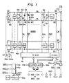
- Fig. 1 is a circuit diagram showing a dynamic RAM in accordance with one embodiment of the present invention.
- Each circuit element or each circuit block shown in the circuit diagram is formed on one semiconductor substrate such as single crystal silicon by a heretofore known production technique for semiconductor integrated circuits, though not particularly limited to that configuration.
- Various MOSFETs formed on the semiconductor substrate are in the enhancement mode. (This also applies to the other embodiments of the invention to be described later.)
- a memory array MARY comprises of a plurality of memory cells arranged in a matrix, a plurality of data lines DL, DL and a plurality of word lines. Though not particularly limited to that configuration, the memory array MARY is of a folded bit line (data line) construction.
- Each of the memory cells MC comprises of a data storage capacitor C s , one of the electrodes of which is connected to a reference potential point such as a power terminal of the circuit, and an address selection MOSFET Qm interposed between this capacitor C S and the data line. Logic "1" and “0" stored in the memory cells are corresponded whether a charge is stored in the capacitor.
- each data line DL, DL of the memory array MARY is first pre-charged by a pre-charge circuit PC to a level substantially close of the power source voltage V cc of the circuit.
- the pre-charge circuit PC comprises, for example, of pre-charge MOSFETs Q c1 and Q c2 that are interposed between the data lines DL, DL and the power terminal V cc , respectively.
- the conduction of these pre-charge transistors MOSFETs Q c1 and Q c2 is controlled by a pre-charge pulse ⁇ pc .
- the pre-charge circuit PC may include an equalizer MOSFET that is interposed between the pair of data lines DL, DL and is controlled by the pre-charge pulse ⁇ pc , in addition to the pre-charge MOSFETs Q c1 and Q c2 .
- One of the plurality of word lines WL of the memory array MARY is selected after each data line has been pre-charged.
- the MOSFET Q m of the memory cell corresponding to the selected word line is turned on and the capacitor C S is coupled to the data line DL or DL . Accordingly, the potential of the data line DL or DL to which the memory cell is connected is changed.
- the potential of the data line DL or DL in this case is changed in accordance with the charge quantity stored in the capacitor C S . This potential change of the data line is sensed by a sense amplifier SA.
- each memory is fabricated so as to be smaller, and a large number of memory cells are coupled to the respective data lines DL, DL. Therefore, the ratio C S /C O of the capacitor C S to the stray capacity C O (not shown) of the common data line DL is extremely small. This means that the potential change applied to the data line DL or DL in response to the charge stored in the capacitor C , that is, a signal, is extremely weak.
- this embodiment includes one dummy cell DC for each data line in the same way as in the well known dynamic RAM in order to detect such a weak signal.
- the dummy cell DC is fabricated under the same production conditions and with the same design constants as those of the memory cell MC except that the capacity of the capacitor C D of the dummy cell DC is half that of the capacitor C s of the memory cell MC.
- the capacitor C D is charged to ground potential by an MOSFET Q d , that receives a timing signal ⁇ d . Since the capacitance of the capacitor C is half that of the capacitor C s , the capacitor C D applies a reference voltage, which is substantially half of the read-out signal from the memory cell MC, to the corresponding data line.
- the symbol SA represents a sense amplifier which amplifies the difference of such potential changes caused by addressing within a sense period that is determined by timing signals (sense amplifier control signals) ⁇ pa1 , ⁇ pa2 .
- the input and output nodes of the sense amplifier are coupled to a pair of complementary data lines DL and DL that are arranged in parallel with each other.
- the number of the memory cells that are connected to these complementary data lines DL, DL, respectively, are made to be equal in order to improve the data detection accuracy at the time of the data read-out operation.
- one of a pair of dummy word lines DWL, DWL is selected so that the dummy cells connected to the other of the data lines are selected correspondingly.
- the sense amplifier SA includes a pair of MOSFETs Q 1 , Q 2 whose gates and drains are cross-connected, and differentially amplifies a weak signal appearing across the complementary data lines DL, DL by these MOSFETs.
- This amplification operation is divided into two stages by an MOSFET Q 7 having relatively small conductance and an MOSFET Q 8 having relatively large conductance.
- the MOSFET Q 7 is rendered conductive by a relatively quick timing signal ⁇ pa1
- the amplification operation of the first stage is actuated in response thereto, and the amplification of the second stage is started at the time at which the potential difference between the complementary data lines DL, DL becomes great to a certain extent and a timing signal ⁇ pa2 is generated.
- the amplification operation of the second stage is started in response thereto.
- the two stage operation of the sense amplifier SA makes it possible to effect amplification devoid of any error of the potential difference between the complementary data lines DL, DL and to effect amplification at a higher operating speed.
- one of the pair of data lines is set to a potential somewhat lower than the power source voltage V cc while the other is set to a low potential substantially equal to the ground potential (0 V) of the circuit.
- the stored data of the memory cell which is once about to be destroyed when addressing is effected, is restored as the high or low level potential obtained by this sense operation is as such supplied to the memory cell MC. In other words, the stored data that has temporarily been read out is written once again into the memory cell.
- An active restore circuit AR is disposed between the complementary data lines DL and DL in order to raise the high level potential re-written into the memory cell MC to a level that is substantially equal to the power source voltage V cc of the circuit.
- This active restore circuit AR has the function of selectively boosting only the high level signal to the power source voltage V cc without affecting at all the low level signal.
- the explanation in detail of the definite circuit construction of this active restore circuit AR is omitted hereby because it is not directly relevant to the gist of the present invention.
- a column switch CW comprising of MOSFETs Q 3 and Q 4 is interposed between the pari of data lines DL, DL and the pair of common complementary data lines CDL, CDL.
- another column switch CW comprising of a similar MOSFETs Q 5 and Q 6 is interposed between the other data line pair and the common complementary data line pair CDL, CDL .
- the input terminals of a data output buffer DOB including an output amplifier and the output terminal of a data input buffer DIB are connected to the common complementary data line pair CDL, CDL.
- a row decoder R-DCR and a column decoder C-DCR receive internal complementary address signals generated by address buffers R-ADB and C-ADB, and generate a selection signal for selecting one word line and one dummy word line as well as a column switch selection signal to be applied to the column switches. Addressing to the memory cells and to the dummy cells is effected in this way.
- the operations of the address buffers R-ADB and C-ADB are controlled by timing signals ⁇ ar and ⁇ ac , respectively, and the operations of the row and column decoders R-DCR and C-DCR are controlled by timing signals ⁇ x and ⁇ y , respectively.
- external address signals AX o - AX i are taken in by the row address buffer R-ADB in synchronism with the timing signal ⁇ ar that is formed on the basis of a row address strobe signal RAS, and the internal address signals generated by the address buffer R-ADB are transferred to the row decoder R-DCR.
- the address decoder R-DCR decodes the internal address signal supplied from the row address buffer A DB, and sets one word line and one dummy word line to a selection level at a timing in accordance with a word line access timing signal ⁇ x .
- External address signals AY o - A Yk are taken in by the column address buffer C-ADB in synchronism with the timing signal ⁇ ac formed on the basis of the column address strobe signal C AS and are transferred to the column decoder C-DCR.
- the column decoder C-DCR generates a column selection signal for selecting a predetermined data line at the timing in accordance with a data line selection timing signal ⁇ y .
- a timing control circuit TC receives the row address strobe signal RAS, the column address strobe signal CAS and a write enable signal WE that are supplied from external terminals, and generates various timing signals necessary for the memory operation besides the timing signals described above as the typical examples.
- the address buffer, address decoder and data output buffer DOB of the column system comprise CMOS (complementary MOS) type static circuits, though they are not particularly limited to this configuration in order to accomplish the lower power consumption of the device and to accomplish continuous read-out operations by bringing the word lines into the accessing state and changing over the column address signals.
- CMOS complementary MOS
- a substrate bias generation circuit V bb -G is actuated by a positive power source voltage such as 5 V that is applied across the power terminal V cc as one of the external terminals of the integrated circuit and the reference potential terminal (or the ground terminal) GND, and generates a negative bias voltage.
- the bias voltage produced from the substrate bias generation circuit V bb -G is supplied to semiconductor regions which are act as a common substrate gate of MOSFET Qm in the memory array and MOSFETs constituting the circuit blocks shown in the drawing.
- the CMOS integrated circuit of this embodiment is formed on the semiconductor substrate which consists of single crystal P-type silicon, but it is not particularly limited to this configuration.
- an N-channel MOSFET such as MOSFET Q m in the memory array MARY is constructed from an N-type source region and an N-type drain region, both formed on the surface of the semiconductor substrate, and a gate electrode which is formed on the surface of the semiconductor substrate between the source region and the drain region via a thin gate insulating film, and which comprises of polysilicon.
- a P-channel MOSFET is formed on an N-type well region formed on the surface of the semiconductor substrate.
- the semiconductor substrate constitutes a common substrate gate for a plurality of N-channel MOSFETs formed thereon.
- the N-type well region constitutes the substrate gate of the P-channel MOSFET formed thereon.
- the substrate gate of the P-channel MOSFET that is, the N-type well region, is coupled to the power terminal V cc of Fig. 1.
- the surface portions other than the surface portions to serve as the active regions that is, the surface portions other than the surface portions on which MOSFETs, MOS capacitors and semiconductor wiring regions are to be formed, as covered by a relatively thick field insulating film, though the film is not shown in the drawing.
- the necessary wiring layer is extended onto the field insulating film or is extended onto the active regions via an insulating film.
- the back-bias voltage -V bb produced from the substrate bias generation circuit V bb -G is supplied to the common substrate gate of the N-channel MOSFETs formed on the surface of the semiconductor substrate.
- the back-bias voltage reduces the junction capacitance formed by the P-N junction between the source-drain regions of the N-channel MOSFETs and the semiconductor substrate and by the P-N junction between the semiconductor wiring regions and the semiconductor substrate. Since the parasitic capacitance which limits the operating speed is thus reduced, the integrated circuit can operate at a higher speed.
- MOSFETs such as the address selection MOSFETs Q m sometimes generate a tailing current or leakage current even when they are turned off.
- the threshold voltage of the MOSFET is increased suitably due to the substrate bias effect when the back-bias voltage -V bb is applied, so that the leakage current decreases. Since the leakage current of the address selection MOSFET Q is reduced, the retention time of the charge stored in the data storage capacitor C s is relatively prolonged.
- a structure of an integrated circuit consisting of a field insulating film and a wiring layer such as a signal wiring layer extending on the field insulating film can be regarded as constituting a part of the parasitic MOSFET structure.
- the back-bias voltage -V bb increases the threshold voltage of the parasitic MOSFET and prevents the operation of the parasitic MOSFET.
- the proportion of the increase of the threshold voltage of MOSFET due to the substrate bias effect decreases with a higher substrate bias voltage. Therefore, the threshold voltage of each N-channel MOSFET remains within a relatively narrow range when the back-bias voltage -V bb is generated, irrespective of the variance of the characteristics of the MOSFETs resulting from the variance developing during the fabrication of the integrated circuit.
- the substrate bias generation circuit Vbb-G periodically generates the bias voltage due to the charge pump action utilizing the capacitor.
- the back-bias voltage is smoothed by the parasitic capacitance and the stray capacitance that exist between the semiconductor substrate to which it is applied, and the power source wiring layer, the semiconductor regions, and the like,
- the back-bias voltage which is retained substantially by the capacitance is reduced by a leakage current that develops between the source-drain region of MOSFET and the semiconductor substrate.
- the leakage current for the semiconductor substrate is not always constant, but is affected by the circuit operation. This leakage current is relatively small so long as the switching state of MOSFET remains unaltered and is kept fixed or stationary. Conversely, if the switching state of MOSFET changes, the leakage current is increased by such a change.
- the mechanism of occurrence of the leakage current to the substrate see "Physics of Semiconductor Devices", p.p. 480 - 487 by S. M. Sze, published by John Wiley & Sons, 1981.
- the substrate leakage current increases when the timing control circuit TC, the address buffers, the decoders, the sense amplifier and the like operate on the basis of the row address strobe signal RAS,the column address strobe signal CAS, and the like.
- the.substrate bias generation circuit Vbb-G has a relatively large driving capacity so that it can keep the substrate bias potential at a suitable value even when the substrate leakage current increases.
- the circuit V bb -G is also designed so as to exhibit low power consumption characteristics.
- the substrate bias generation circuit V bb -G of this embodiment includes a circuit portion exhibiting a steady operation and a circuit portion exhibiting an intermittent operation, from the aspect of its driving capacity and its power consumption.
- the circuit portion exhibiting the steady operation is provided with the driving capacity such that when each circuit shown in F ig. 1 is substantially in the non-operating state, it can keep the back-bias voltage -V bb at a desired value.
- the circuit portion exhibiting the intermittent operation is provided with a relatively large driving capacity so that the back-bias voltage can be kept at a desired values even when the substrate leakage current is increased.
- a level detection circuit VLD such as shown in Fig. 1 is provided in order to control the operation of the circuit portion exhibiting the intermittent operation.
- the level detection circuit VLD detects the back-bias voltage -V bb' and produces a signal for operating the circuit portion of the intermittent operation when the back-bias voltage is lower than a desired level.
- the operation of the circuit portion exhibiting intermittent operation in the substrate bias generation circuit in accordance with this embodiment is also controlled by a relatively fast row.system control signal RAS 1 which is produced from the timing control circuit TC on the basis of the external control signal RAS.
- the back-bias voltage is controlled in such a manner as to again assume the desired level by a feedback route consisting of the level detection circuit VLD and the circuit portion exhibiting the intermittent operation, even when the operation control of the substrate bias generation circuit by the control signal RAS1 does not exist. In this case, . however, the time required before the back-bias voltage returns to the desired level becomes somewhat long in accordance with the change of speed of the output of the circuit portion exhibiting the intermittent operation.
- control signal RAS that is, the control signal having a quicker timing among the row system control signals produced from the timing control circuit TC
- the operation of the circuit portion exhibiting intermittent operation can be started at the timing which is substantially the same as the timing at which the substrate leakage current is drastically increased.
- the drastic level change of the back-bias voltage can be prevented.
- the level detection circuit VLD can be omitted.
- the following must be taken into consideration in such a case.
- the back-bias voltage can change from 0 volt to the desired level within a relatively short period after the power source has been turned on.
- the circuit portion exhibiting the intermittent operation in the substrate bias generation circuit V bb -G be also operated.
- the row address strobe signal for executing the dummy operation cycle must be applied to the external terminal RAS at the same time that the power is turned on.
- the circuit portion exhibiting the intermittent operation is immediately rendered operative by the detection output, so that the back-bias voltage is changed to the predetermined level within a relatively short period from the time that - the power source is turned on, irrespective of the signal applied to the external terminal RAS.
- the level of the back-bias voltage might be reduced undesirably due to the increase of the substrate leakage current resulting from the rise of the operating temperature of the integrated circuit.
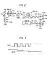
- Fig. 2 is a circuit diagram showing an example of the substrate bias generation circuit Vbb-G together with that of the level detection circuit VLD described above.
- those MOSFETs which are provided with straight lines between their sources and drains are of the P-channel type, while those MOSFE T s which are expressed by ordinary symbols are of the N-channel type.
- the back-bias voltage generation circuit V bb -G1 of the steady operation comprises of an oscillation circuit OSC2, CMOS inverter circuits IV4, IV5 for waveform shaping and amplifying the output of the oscillation circuit and a rectification circuit.
- the oscillation circuit OSC2 comprises- for example, of a ring oscillator which is operated by the power source voltage V cc and comprises of a plurality of CMOS inverter circuits that are coupled with one another in a ring configuration.
- the rectification circuit comprises of a charge pump capacitor C2 and MOSFETs Q 20 , Q 21 whose gate electrodes are connected to their drain electrodes (which operate either as the drain electrodes or as the source electrodes depending upon the polarity of the voltage applied thereto, but are called hereby the drain electrodes) so that the transistors function as the rectification elements.
- the capacitor C2 has an MOS capacitor structure having a similar structure to the N-channel MOSFET.
- one of the electrodes of the capacitor which should correspond to the gate electrode of the MOSFET is coupled to the output terminal of the CMOS inverter circuit IV 5 as the output buffer.
- the other of the electrodes of the capacitors C 2 that is, the electrode that should correspond to the source or drain electrode of the MOSFET, is coupled to the common junction between the MOSFETs Q 20 and Q 21 .
- the MOSFET Q 20 which acts as the rectification element is interposed between the other electrode of the capacitor C 2 and the grounding point GND of the circuit, and the MOSFET Q 21 is disposed between the other electrode of the capacitor C 2 and the semiconductor substrate.
- a parasitic capacitance C sb (not shown), that retains substantially the back-bias voltage, exists between the substrate and the grounding point of the circuit.
- the MOSFET Q 20 of the diode form is turned on when the oscillation pulse produced from the inverter circuit IV5 is at the high level (substantially at the level of the power source voltage V ), and the capacitor C 2 is pre-charged by the output high level.
- the output pulse is at the low level (substantially at the level of the ground potential of the circuit)
- the other electrode of the capacitor C 2 is at a negative potential of -(V cc - V th ).
- the symbol V th represents the threshold voltage of the MOSFET Q 20 .
- the MOSFET Q 21 of the diode form is turned on by this negative potential and transmits the negative potential to the parasitic capacitance C sb described above.
- the substrate bias voltage generation circuit V bb -G1 of the steady operation has a relatively small current supply capacity such that when the RAM described above is under the chip non-selection state, it can compensate for the leakage current flowing through the substrate.
- the current supply capacity of the substrate bias voltage generation circuit Vbb-Gl of the steady operation is determined substantially by the capacitance of the capacitor C 2 and the oscillation frequency of the oscillation circuit OSC.
- the quantity of the charge injected into the semiconductor substrate in response to one oscillation output becomes greater with with a greater capacitance of the capacitor C 2 .
- the number of times of the charge injection into the semiconductor substrate per unit time becomes greater with a higher oscillation frequency of the oscillation circuit OSC 2 .
- the substrate bias voltage generation circuit of the steady operation is constituted in such a fashion as to exhibit low power consumption characteristics while securing a necessary and relatively small current supply capacity.
- the oscillation frequency of the oscillation circuit OSC 2 is set to be a relatively low value such as 1 or 2 M Hz by selecting a suitable number of CMOS inverter - circuits-forming the oscillation circuit and by setting their signal delay characteristics to suitable levels.
- the power consumed by the oscillation circuit OSC 2 is proportional to the oscillation frequency.
- the operation current or consumed current of each CMOS inverter circuit constituting the oscillation circuit OSC 2 is proportional to a so-called "transient current" necessary for the charge and discharge of the load capacitance (consisting of wiring capacity, input capacitance of inverter circuits of the post stage and the like) coupled to the output of each inverter circuit in the same way as in the well known CMOS inverter circuit, and is substantially zero in the stationary state in which the output or input of each inverter is at the high or low level. Since the transient current of each CMOS inverter circuit is proportional to the operation frequency, the power consumption of the oscillation circuit OSC 2 having a low oscillation frequency is low.
- the driving capacity of the CMOS inverter circuit IV 5 as the output buffer for driving the rectification circuit may be relatively small because the capacitor C 2 is relatively small. Therefore, the P- and N-channel MOSFETs, not shown, constituting this CMOS inverter circuit IV 5 need not have low ON resistance; hence, may be small.
- the P- and N-channel MOSFETs, not shown, constituting the CMOS inverter circuit IV 4 as the waveform shaping circuit need only drive a load having a relatively small capacitance becuase the MOSFETs constituting the CMOS inverter circuit IV S are small. Therefore, the MOSFETs constituting the CMOS inverter circuit IV 4 may be small.
- the substrate bias generation circuit V bb -G 2 for intermittent operation comprises of a controllable oscillation circuit, that is, an oscillation circuit OSC 1 capable of the intermittent operation, a CMOS inverter circuit IV 2 as a waveform shaping circuit, a CMOS inverter circuit IV 3 as an output buffer and a rectification circuit.
- the oscillation circuit OSC comprises of C M OS NAND gate circuits G 2 through G 4 .
- the output terminals of these gate circuits G 2 - G4 are connected to one of the input terminals of a gate circuit of the post stage.
- the output terminal of the gate circuit G 4 of the final stage is connected to one of the input terminals of the gate circuit G 2 of the initial stage.
- the other input terminal of each of the gate circuits - G 2 - G 4 is regarded as a common operation control terminal and is connected to the output terminal of the gate circuit G 1 .
- Each of the gate circuits G 2 - G 4 constituting the oscillation circuit OSC 1 operates substantially as an inverter when the control signal supplied to the operation control terminal is at the high level (logic "1") such as one that is substantially equal to the power source voltage V cc . Therefore, the oscillation circuit OSC 1 performs the oscillation operation as a ring oscillator. When the control signal is at the low level (logic "0") such as one that is substantially equal to the ground potential, the output of each of the gate circuits G 2 - G 4 is kept fixed at the high level which is substantially equal to the power source voltage V cc .
- the rectification circuit comprises of a capacitor C 1 and MOSFETs Q 18 , Q 19 as shown in the drawing.
- the rectification circuit comprising of the capacitor C 1 and the M OS FE Ts Q 18 , Q 19 is operated in response to the former, and the charge for applying a back-bias voltage is injected into the semiconductor substrate.
- the back-bias voltage in this case is determined by the substrate bias voltage generation circuit V bb -G 1 of the steady operation with the substrate bias voltage generation circuit V bb -G 2 .
- the rectification circuit comprising of the capacitor C 1 and the MOSFETs does not operate.
- the output of the CMOS inverter circuit IV 3 is kept at the high level substantially equal to the power source voltage V cc by the high level output of the oscillation circuit OSC 1 .
- the capacitor C 1 is kept in the charge state by the high level output of the .inverter IV 3 .
- the CMOS NAND gates G 2 - G 4 constituting the oscillation circuit OSC do not consume current so long as they are in the stationary state, in the same way as the CMOS inverter circuit. Therefore, the power consumed by the substrate bias voltage generation circuit V bb -G 2 of the intermittent operation is substantially zero during the period in which the oscillation circuit OSC 1 stops operating.
- the substrate back-bias voltage generation circuit V bb -G 2 operating intermittently must have a relatively large current supply capacity so that it can compensate for a relatively large leakage current that flows to the substrate when the RAM is in the operative state. Therefore, the capacitance of the capacitor C 1 is relatively large, while the oscillation frequency of the oscillation circuit OSC 1 is relatively large such as from 10 to 15 MHz.
- the P- and N-channel MOSFETs, not shown, that constitute the CMOS inverter circuit IV 3 are relatively large because the rectification circuit constitutes a relatively heavy load.
- the P- and N-channel MOSFETs, not shown, that constitute the CMOS inverter circuit IV 2 are relatively large so that they can sufficiently drive the C M OS inverter circuit IV 3 .
- This embodiment includes a level detection circuit VLD comprising of MOSFETs Q 10 - Q 17 and CMOS inverter circuits IV 0 , IV 1 , and a control circuit comprising of the CMOS NAND gate circuit G 1 in order to operate the substrate bias voltage generation circuit Vbb-G2 only when the operation is necessary.
- VLD level detection circuit
- CMOS inverter circuits IV 0 , IV 1 CMOS inverter circuits
- the level detection circuit VLD is provided in order to positively detect excess substrate back-bias voltage -V bb beyond a predetermined level necessary for high speed operation of the RAM.
- the ground potential of the circuit is steadily applied to the gate of the P-channel MOSFET Q 10 so that the transistor serves as a constant current load.
- the MOSFET Q 10 is constantly turned on.
- a P-channel MOSFET Q 11 for level clamping is connected in series with this MOSFET Q 10 . Since the ground potential of the circuit is constantly applied to the gate, this MOSFET Q11 is constantly kept ON.
- the source potential of the MOSFET Q 11 ' that is, the potential of the electrode coupled to the drain of the MOSFET Q 10 , is at the level which is higher than at least the ground potential of the circuit, and the drain potential is substantially equal to the ground potential of the circuit.
- MOSFETs Q 12 - Q 14 in the diode form are connected in series between the drain of the MOSFET Q 11 and the substrate (-V bb ).
- the detection level of the level detection circuit VLD is substantially equal to the sum 3V th of the threshold voltages V th of the three MOSFETs Q 12 through Q 14 connected in series. If the substrate back-bias voltage -V bb is at the level lower than the total threshold voltage 3V th of the three transistors Q 12 - Q 14 in the diode form, these transistors are turned off. In this case, the potential at the junction between the MOSFETs Q 11 and Q 10 is at the high level such as the power source voltage V cc .
- the substrate back-bias voltage -V bb is at the level higher than the level of the total threshold voltage 3V th of the MOSFETs Q 12 - Q 14 in the diode form, these transistors Q 12 - Q 14 are turned on.
- the potential at the junction between the MOSFETs Q 11 and Q 10 is at the low level which is higher by the threshold voltage V th of the MOSFET Q 11 than the ground potential of the circuit.
- the current flowing from the power source terminal V cc to the substrate positively reduces the substrate back-bias voltage -V bb .
- the conductance of the load MOSFET Q 10 is set to an extremely small value in order to minimize the current flowing to the substrate through the level detection circuit and to sufficiently reduce the low level appearing at the junction between the MOSFETs Q 10 and Q 11 .
- the conductance is set to an extremely small conductance so that the MOSFET Q 10 permits the flow of only a slight current.
- CMOS inverter circuit constituted by a P-channel MOSFET Q 15 and an N-channel MOSFET Q 16 .
- the inverter circuit comprising of the MOSFET Q 15 and Q16 forms a Schmidt circuit (hysteresis circuit) together with an MOSFET Q 17 and a CMOS inverter circuit IV in order to realize a 0 high speed change of the detection output to be obtained and particularly, to operate the oscillation circuit OSC 1 rapidly when the back-bias voltage is reduced.
- the output of the inverter circuit comprising of the MOSFETs Q 15 and Q 16 is a p- plied to the input of the CMOS inverter circuit IV o having a similar construction.
- the output of this CMOS inverter circuit IV o is applied to the gate of the P-channel MOSFET Q 17 disposed between its input and the power source voltage V cc , thereby effecting positive feedback.
- the detection signal produced from the inverter circuit IV 0 is changed to the low level at a high speed.
- the detection output generated by this inverter circuit IV o is applied to one of the input terminals of the CMOS NAND gate circuit G 1 through the CMOS inverter circuit IV 1 .
- the internal row address strobe signal RAS 1 formed by the timing control circuit TC shown in Fig. 1 is applied to the other input terminal of this NAND gate circuit G 1 .
- the output of this NAND gate circuit G 1 is applied in - common to the other input terminals of the NAND gate circuits G 2 - G 4 that constitute the ring oscillator OSC 1 described above.
- the output of the gate circuit G 1 responds to the detection output of the level detection circuit VLD.
- the absolute value of the substrate back-bias voltage -V bb is less than that of the total threshold voltage 3V th of the three MOSFETs Q 12 through Q 14 described already, these transistors are turned off; hence, the detection output is at the high level. Therefore, the detection output supplied to the NAND gate circuit G 1 is at the low level (logic "0"), and the output of the NAND gate circuit G 1 is at the high level (logic "1"), whereby the oscillation circuit OSC 1 is in the oscillating state.
- the absolute value of the substrate back-bias voltage is increased by the rectification circuit that receives the output pulses of the oscillation circuit.
- the MOSFETs Q 12 - Q 14 are turned on, so that the detection output is at the low level, whereupon the detection output supplied to the NAND gate circuit G 1 is at the high level (logic "1"). Since the output of the NAND gate circuit G 1 falls to the low level (logic "0") in response to the former, the outputs of all the NAND gate circuits G 2 - G 4 constituting the oscillation circuit OSC rise to the high level (logic "1"). In other words, oscillation stops.
- the operation of the rectification circuit (C 1 , Q 18 , Q 19 ) also stops. Since the oscillation circuit consuming much power and the rectification circuit thus stop operating, lower power consumption can be accomplished. Incidentally, since the substrate back-bias voltage is at a low level at or near ground potential immediately after turning on the power, the operations of both substrate back-bias voltage generation circuits can quickly raise the absolute value of the substrate back-bias voltage to the desired level.
- the oscillation circuit OSC 1 When the row address strobe signal RAS falls to the low level and chip selecting is thus indicated, the internal signal RAS 1 is lowered to the low level in response thereto, so that the output of the NAND gate circuit G 1 rises to the high level (logic "1") irrespective of the detection otuput of the level detection circuit described above.
- the oscillation circuit OSC 1 When the RAM executes the write-in/read-out operations and the like, the oscillation circuit OSC 1 is rendered unconditionally operative. This is to prevent the drastic drop of the absolute value of the substrate back-bias voltage -V bb that is caused by a relatively great substrate leakage current occurring when RAM operations such as described above are started. If the oscillation circuit OSC 1 is rendered operative in advance before the RAM is rendered operative as in this embodiment, it becomes possible to prevent the drastic drop of the substrate back-bias voltage -V bb .
- Fig. 4 is a circuit diagram showing a dynamic RAM in accordance with the second embodiment of the invention. Those circuits which are not shown in Fig. 4 are substantially the same as those shown in Fig. 1.
- the RAM in this embodiment includes a refresh control circuit REFC and a multiplexer MPX to accomplish the automatic refresh of memory cells.
- the refresh control circuit REFC includes a refresh timer and a refresh address counter that are not shown.
- the refresh timer is operated when the row address strobe signal RAS is raised to the high level and the refresh control signal REFH is lowered to the low level, that is, when the refresh operation is indicated in the chip non-selecting state, and produces periodically refresh control signals ⁇ ref during its operation.
- the refresh address counter receives the control signals produced from the refresh timer as its advance pulses, and forms refresh address signals ax 0 through ax i .
- the operation of the multiplexer MPX is controlled by the control signal ⁇ ref .
- the multiplexor MPX selects the internal address signals ax 0 through ax i produced from the address buffer R-ADB when the control signal ⁇ ref is not produced, and selects the refresh address signals ax o ' through ax . ' when the control signal ⁇ ref is produced.
- the timing control circuit TC generates various timing signals similar to those of the first embodiment in response to the row address strobe signal RAS, the column address strobe signal C A S, and the like that are supplied to the external terminals, in the same way as in the first embodiment.
- this embodiment is somewhat different from the first embodiment in that the internal circuit of the timing control circuit TC is constructed in such a fashion as to respond to the refresh control signal ⁇ ref .
- the timing control signal TC controls the operations of the row system circuits, that is, the row address decoder R-DCR, the pre-charge circuit PC, the sense amplifier SA and the active restore circuit AR, shown in Fig. 1, in response to the refresh control signal.
- the refresh operation is effected whenever the refresh control signal ⁇ ref is generated.
- the refresh control signal ⁇ ref when the refresh control signal ⁇ ref is generated, the refresh address signals ax 0 through ax i of the refresh address counter are supplied to the row address decocer R-DEC of F ig. 1 through the multiplexor MPX in response to the refresh control signal ⁇ ref.
- the control signal ⁇ ref actuates the timing control circuit TC, and the row system timing signals produced by the timing control circuit TC in turn actuate sequentially the pre-charge circuit PC, the row address decoder R-DCR, the sense amplifier SA and the active restore circuit AR of Fig. 1.
- the word line corresponding to the refresh address is selected, and the stored data of the memory cell coupled to the selected word line is refreshed.
- the substrate bias voltage generation circuit V bb -G and the level detection circuit VLD of this embodiment are substantially the same as those of Fig. 2.
- a logic synthesis circuit comprising of a CMOS gate circuit G 5 and CMOS inverter circuits IV 6 and IV 7 is provided so that the operation of the substrate bias voltage generation circuit V bb -G is controlled by the refresh control signal ⁇ ref , too.
- the output of this logic synthesis circuit is set to the low level at the time of chip selection (a period in which the row address strobe signal RAS is at the low level) and at the time of the refresh operation.
- the circuit portion of the intermittent operation inside the substrate bias voltage generation circuit V bb -G is operated synchronously when the substrate leakage current is increased by the execution of the refresh operation, that is, when the timing control circuit TC and the row system circuits are operated by the refresh control signal ⁇ ref .
- a power source device PS for forming a predetermined d.c. voltage from a commercial a.c. power source, for example, and a series circuit comprising of a battery E and a diode D are connected between the external terminal V cc and GND.
- the power source device PS is cut off, the power source voltage required by the RAM for holding the information or data is supplied from the battery E.
- the refresh operation at the time of battery back-up is automatically executed without requiring any external control signals, in particular. Therefore, the RAM does not require the operations of other external devices at the time of battery back-up.
- Fig. 5 is a circuit diagram showing a level detection circuit VLD and a'substrate bias voltage . generation circuit in accordance with still another embodiment of the invention.
- the level detection circuit VLD comprises of a P-channel MOSFET Q 26 , N-channel MOSFETs Q 27 - Q 29 and a CMOS inverter circuit IV 10 as shown in the drawing.
- the substrate gate of the MOSFET Q 26 is connected to the power terminal V cc in the same way as in the foregoing embodiments.
- the substrate gates of the MOSFETs Q 27 Q 29 consist of the P-type semiconductor substrate.
- the detection output VD of the level detection circuit VLD is set to the high level substantially equal to the V cc level or to the low level substantially equal to 0 V in accordance with the level of the back-bias voltage -V bb in the same way as in the foregoing embodiments.
- the CMOS NAND gate circuit G 6 receives the detection output VD of the level detection circuit VLD and the control signal VCN 1 .
- the control signal VCN 1 is generated by an inverter circuit IV 7 shown in Fig. 4, for example.
- the output of the gate circuit G 6 is supplied to the substrate bias voltage generation circuit Vbb-G.
- the substrate bias voltage generation circuit V bb -G comprises of the common oscillation circuit OSC, a C M OS inverter circuit IV 8 which act as a waveform shaping circuit, a CMOS NAND gate circuit G 7 , aCMOS inverter circuit IV 11 , CMOS inverter circuits IV 9 and IV 12 as a buffer amplifier, and rectification circuits CPC 1 and CPC 2 .
- CMOS inverter circuit IV 8 Since the output of the CMOS inverter circuit IV 8 is directly supplied to the input of the CMOS inverter circuit IV 9 , the latter generates steady pulse signals. In consequence, the rectification circuit CPC 1 is operated steadily.
- the output of the CMOS inverter circuit IV 8 is supplied to the input of the CMOS inverter circuit IV 12 through the gate circuit G 7 and the CMOS inverter circuit IV 11 . Therefore, the output pulses of the CMOS inverter circuit IV 12 are intermittent.
- the rectification circuit CPC 2 is therefore operated intermittently in accordance with the output'of the inverter circuit IV 12 .
- the current supply capacity of the rectification circuit CPC 1 exhibiting the steady operation to the semiconductor substrate may be small in the same way as in the foregoing embodiments. Therefore, the charge pump capacitor C 3 may also be relatively small.
- the charge pump capacitor in the rectification circuit CPC 2 exhibiting the intermittent operation, is relatively large.
- capacitors C 3 and C 4 are formed in an N-type region (not shown) that is in turn formed on the surface of the P-type semiconductor substrate, and have a construction similar to that of the P-channel MOSFET.
- the N-type well region in which these capacitors C 3 and C 4 are formed is held at the potential of the power terminal V cc of the circuit, for example. This - construction is somewhat advantageous for reducing the substrate leakage current.
- the oscillation circuit OSC is common to the rectification circuits CPC 1 and CPC 2 .
- the bias current supplied to the semiconductor substrate is associated with the operating frequency of the rectification circuit.
- the oscillation frequency of the oscillation circuit OSC is determined by the current supply capacity provided by the rectification circuit CPC of the steady operation and by the current supply capacity provided by the rectification circuit CPC 2 of the intermittent operation. Therefore, the lower limit of the oscillation frequency of the oscillation circuit OSC is somewhat limited in comparison with that of the oscillation circuit OSC 2 of the steady operation shown in Fig. 2.
- this embodiment does not include an oscillation circuit which consumes power during the operation of its own, such as the oscillation circuit OSC 1 of the intermittent operation shown in Fig. 2.
- the number of necessary circuit elements can be reduced. Furthermore, the average power consumption of the RAM as a whole can be sufficiently reduced even when the power consumed by the common oscillation circuit OSC is somewhat greater than that of the oscillation circuit OSC 2 of Fig. 2, for example.
- Fig. 6 is a circuit diagram of the substrate bias voltage generation circuit V bb -G in accordance with still another embodiment of the present invention.
- the substrate bias voltage generation circuit V bb -G of this embodiment comprises of the oscillation circuit OSC, a CMOS inverter circuit IV 3 which act as a waveform shaping circuit, a CMOS NAND gate circuit G 8 , CMOS inverter circuits IV 14 and IV 16 , CMOS inverter circuits IV15 and IV17 which act as buffer amplifier, charge pump capacitors C 5 and C 6 and N-channel MO SFETs Q35 through Q 38 as rectification elements.
- the circuit operation when the control signal VCN 2 formed in combination with the detection output of the level detection circuit and the control signal of the dynamic RAM as in the foregoing embodiment is at the low level, is as follows.
- the outputs of the gate circuit G 8 and inverter circuit IV 17 are at the high level irrespective of the output of the oscillation circuit OSC.
- the capacitor C 6 is under the charge state by the high level output of the inverter IV 17 .
- the output of the inverter IV 15 is charged to the high and low levels in accordance with the output of the oscillation circuit OSC.
- the rectification circuit comprising of the capacitor C 5 and the MOSFETs Q 37 and Q 38 is operated, and the back-bias voltage -V bb is supplied to the semiconductor substrate in response thereto.
- the MOSFET Q 35 is kept substantially OFF because the maximum positive potential level appearing at the node N i is clamped by the MOSFET Q 37 as the rectification element.
- the circuit operation when the control signal VCN 2 is at the high level is as follows.
- the output of the inverter circuit IV 13 is raised to the high level in accordance with the output of the oscillation circuit OSC, the output of the inverter circuit IV 15 is raised to the high level substantially equal to the power source voltage V cc in response thereto, while the output of the inverter circuit IV 17 is lowered to the low level substantially equal to 0 V. Since the capacitor C 6 is charged in advance, the node N 2 is set to the negative potential when the output of the inverter circuit IV 17 is lowered to the low level. As the node N 2 is thus at the negative potential, the MOSFET Q 35 as the rectification element is rendered conductive. As a result, the negative potential formed by the capacitor C 6 is transmitted to the node-N 1 through the MOSFET Q 35 .
- the capacitor C 5 is charged by the high level produced from the inverter circuit IV 15 and by the negative potential applied to the node N 1 to such a high level as to exceed the power source voltage V cc .
- the capacitor C 6 is operated substantially as a bootstrap capacitor and the charging voltage of the capacitor C 5 is at the boost level.
- the output of the inverter circuit IV 15 is lowered to the low level substantially equal to 0 V in response thereto. Since the capacitor C 5 is charged in advance to the boost level, the node N 1 is set to a large negative potential in response to the drop of the output of the inverter circuit IV 15 to the low level. The potential of this node N 1 is supplied to the semiconductor substrate via the MOSFET Q 38 . The output of the inverter circuit IV 17 is raised to the high level substantially equal to the power source voltage in accordance with the low level output of the inverter circuit IV 13 . The MOSFET Q 36 is rendered conductive by the positive potential given to the node N 2 through the capacitor C 6 . As a result, the capacitor C 6 is charged again.
- the two inverter circuit IV 15 and IV 17 having a relatively large driving capacity are operated so as to complement each other so that the transient current flowing through the power source wiring inside the RAM can be reduced, and noise in the power source wiring can be therefore reduced.
- the invention has thus been described definitely with reference to some preferred embodiments thereof, the invention is not particularly limited thereto, but can of course be modified or changed in various manners without departing from the gist thereof.
- the monitor output of the substrate back-bias voltage may be made invalid by the chip selection signal in place of the internal control signal RAS ⁇ in the circuit of the embodiment shown in Fig. 2.
- the oscillation circuit which is operated steadily by turning on the power source voltage and its rectification circuit are not essentially necessary.
- the circuit construction in which the substrate bias generation circuit is divided into the circuit portion exhibiting the steady operation and the circuit portion exhibiting the intermittent operation is desirable from the aspect of the prevention of the unnecessary increase of the sizes of the circuit elements forming the circuit portion exhibiting the intermittent operation. If necessary, however, the circuit having a small current supply capacity and the circuit having a large current supply capacity may be operated selectively. A plurality of circuit portions exhibiting the intermittent operation may be disposed and may be controlled individually.
- the term "substrate” of the “substrate bias generation circuit” means one semiconductor region such as the substrate gate of a field effect element but is not intended to mean only a semiconductor substrate.
- the term "substrate” means that P-type well region.
- the reference voltage for reading out the memory cells constituting the dynamic RAM may be formed by short- circuiting the complementary data lines that are at the high and low levels under the high impedance state, without using the dummy cells.
- the reference voltage in this case is at the intermediate level.
- peripheral circuits such as the address buffers, the address decoders, and the like may be constituted by CMOS static circuits.
- the X and Y address signals may be supplied from mutually independent external terminals and a detection circuit for detecting the change timing of the address signal is disposed in order to generate various timing signals necessary for the operations of the internal circuits.
- the present invention can be applied widely to semiconductor integrated circuit devices equipped with a built-in substrate bias generation circuit.
Landscapes
- Engineering & Computer Science (AREA)
- Microelectronics & Electronic Packaging (AREA)
- Computer Hardware Design (AREA)
- Power Engineering (AREA)
- Dram (AREA)
- Semiconductor Integrated Circuits (AREA)
Applications Claiming Priority (3)
| Application Number | Priority Date | Filing Date | Title |
|---|---|---|---|
| JP59180534A JPS6159688A (ja) | 1984-08-31 | 1984-08-31 | 半導体集積回路装置 |
| JP180534/84 | 1984-08-31 | ||
| SG157794A SG157794G (en) | 1984-08-31 | 1994-10-27 | Semiconductor integrated circuit device |
Publications (3)
| Publication Number | Publication Date |
|---|---|
| EP0173980A2 true EP0173980A2 (de) | 1986-03-12 |
| EP0173980A3 EP0173980A3 (en) | 1989-12-06 |
| EP0173980B1 EP0173980B1 (de) | 1992-11-04 |
Family
ID=26500026
Family Applications (1)
| Application Number | Title | Priority Date | Filing Date |
|---|---|---|---|
| EP85110960A Expired - Lifetime EP0173980B1 (de) | 1984-08-31 | 1985-08-30 | Integrierte Halbleiterschaltungsanordnung |
Country Status (6)
| Country | Link |
|---|---|
| US (3) | US4775959A (de) |
| EP (1) | EP0173980B1 (de) |
| JP (1) | JPS6159688A (de) |
| KR (5) | KR940001638B1 (de) |
| HK (1) | HK85295A (de) |
| SG (1) | SG157794G (de) |
Cited By (5)
| Publication number | Priority date | Publication date | Assignee | Title |
|---|---|---|---|---|
| US4794278A (en) * | 1987-12-30 | 1988-12-27 | Intel Corporation | Stable substrate bias generator for MOS circuits |
| US4843256A (en) * | 1986-12-23 | 1989-06-27 | Jenoptik Jena Gmbh | Controlled CMOS substrate voltage generator |
| DE3924952A1 (de) * | 1988-08-26 | 1990-03-01 | Mitsubishi Electric Corp | Substratvorspannungsgenerator in einem dynamischen schreib-lese-speicher mit einer selbstauffrischfunktion und verfahren zum erzeugen einer substratvorspannung in einem derartigen speicher |
| FR2648291A1 (fr) * | 1989-06-10 | 1990-12-14 | Samsung Electronics Co Ltd | Convertisseur de tension interne dans un circuit integre a semi conducteur |
| KR20140129284A (ko) * | 2012-03-31 | 2014-11-06 | 인텔 코오퍼레이션 | 지연 보상 에러 표시 신호 |
Families Citing this family (81)
| Publication number | Priority date | Publication date | Assignee | Title |
|---|---|---|---|---|
| JPS6159688A (ja) * | 1984-08-31 | 1986-03-27 | Hitachi Ltd | 半導体集積回路装置 |
| JPH0618249B2 (ja) * | 1984-10-17 | 1994-03-09 | 富士通株式会社 | 半導体集積回路 |
| US5249159A (en) * | 1987-05-27 | 1993-09-28 | Hitachi, Ltd. | Semiconductor memory |
| KR900006192B1 (ko) * | 1987-10-30 | 1990-08-25 | 삼성전자 주식회사 | 백 바이어스 전압 발생기 |
| JP2824470B2 (ja) * | 1988-07-05 | 1998-11-11 | 株式会社日立製作所 | ダイナミック型ram |
| KR0134773B1 (ko) * | 1988-07-05 | 1998-04-20 | Hitachi Ltd | 반도체 기억장치 |
| IT1225608B (it) * | 1988-07-06 | 1990-11-22 | Sgs Thomson Microelectronics | Regolazione della tensione prodotta da un moltiplicatore di tensione. |
| JPH0814986B2 (ja) * | 1988-12-08 | 1996-02-14 | 三菱電機株式会社 | リフレッシュ機能内蔵ダイナミック型半導体記憶装置 |
| JPH0817033B2 (ja) * | 1988-12-08 | 1996-02-21 | 三菱電機株式会社 | 基板バイアス電位発生回路 |
| JPH02215154A (ja) * | 1989-02-16 | 1990-08-28 | Toshiba Corp | 電圧制御回路 |
| US5341035A (en) * | 1990-06-04 | 1994-08-23 | Matsushita Electric Industrial Co., Ltd. | Substrate potential generator |
| US5039877A (en) * | 1990-08-30 | 1991-08-13 | Micron Technology, Inc. | Low current substrate bias generator |
| FR2668668B1 (fr) * | 1990-10-30 | 1994-02-04 | Samsung Electronics Co Ltd | Generateur de tension de substrat pour un dispositif a semiconducteurs. |
| JP2724919B2 (ja) * | 1991-02-05 | 1998-03-09 | 三菱電機株式会社 | 基板バイアス発生装置 |
| JPH04255989A (ja) * | 1991-02-07 | 1992-09-10 | Mitsubishi Electric Corp | 半導体記憶装置および内部電圧発生方法 |
| JPH04259983A (ja) * | 1991-02-15 | 1992-09-16 | Hitachi Ltd | 半導体記憶装置 |
| US5196739A (en) * | 1991-04-03 | 1993-03-23 | National Semiconductor Corporation | High voltage charge pump |
| KR940004482Y1 (ko) * | 1991-10-10 | 1994-07-04 | 금성일렉트론 주식회사 | 셑 플레이트 전압 초기 셑업회로 |
| DE4237589C2 (de) * | 1991-11-07 | 1999-10-28 | Samsung Electronics Co Ltd | Spannungspumpschaltung |
| KR940008147B1 (ko) * | 1991-11-25 | 1994-09-03 | 삼성전자 주식회사 | 저전력 데이타 리텐션 기능을 가지는 반도체 메모리장치 |
| US5260646A (en) * | 1991-12-23 | 1993-11-09 | Micron Technology, Inc. | Low power regulator for a voltage generator circuit |
| KR950002015B1 (ko) * | 1991-12-23 | 1995-03-08 | 삼성전자주식회사 | 하나의 오실레이터에 의해 동작되는 정전원 발생회로 |
| DE4221575C2 (de) * | 1992-07-01 | 1995-02-09 | Ibm | Integrierter CMOS-Halbleiterschaltkreis und Datenverarbeitungssystem mit integriertem CMOS-Halbleiterschaltkreis |
| KR950003390Y1 (ko) * | 1992-09-24 | 1995-04-27 | 문정환 | 로우 어드레스 스트로브(/ras) 신호의 클램핑 회로 |
| KR950006067Y1 (ko) * | 1992-10-08 | 1995-07-27 | 문정환 | 반도체 메모리 장치 |
| JPH06195971A (ja) * | 1992-10-29 | 1994-07-15 | Mitsubishi Electric Corp | 基板電位発生回路 |
| JPH07105681A (ja) * | 1993-10-07 | 1995-04-21 | Mitsubishi Electric Corp | 半導体装置 |
| JP3110262B2 (ja) * | 1993-11-15 | 2000-11-20 | 松下電器産業株式会社 | 半導体装置及び半導体装置のオペレーティング方法 |
| US5461591A (en) * | 1993-12-02 | 1995-10-24 | Goldstar Electron Co., Ltd. | Voltage generator for semiconductor memory device |
| JP3090833B2 (ja) | 1993-12-28 | 2000-09-25 | 株式会社東芝 | 半導体記憶装置 |
| US6882215B1 (en) * | 1994-01-21 | 2005-04-19 | Samsung Electronics Co., Ltd. | Substrate bias generator in semiconductor memory device |
| KR0123849B1 (ko) * | 1994-04-08 | 1997-11-25 | 문정환 | 반도체 디바이스의 내부 전압발생기 |
| US5502671A (en) * | 1994-08-31 | 1996-03-26 | Texas Instruments Incorporated | Apparatus and method for a semiconductor memory configuration-dependent output buffer supply circuit |
| JP3167904B2 (ja) * | 1994-12-27 | 2001-05-21 | 日本鋼管株式会社 | 電圧昇圧回路 |
| US5670907A (en) * | 1995-03-14 | 1997-09-23 | Lattice Semiconductor Corporation | VBB reference for pumped substrates |
| JPH08272467A (ja) * | 1995-03-31 | 1996-10-18 | Mitsubishi Electric Corp | 基板電位発生回路 |
| DE69632098T2 (de) * | 1995-04-21 | 2005-03-24 | Nippon Telegraph And Telephone Corp. | MOSFET Schaltung und ihre Anwendung in einer CMOS Logikschaltung |
| KR0142967B1 (ko) * | 1995-04-26 | 1998-08-17 | 김광호 | 반도체 메모리장치의 기판 전압 제어회로 |
| US6259310B1 (en) * | 1995-05-23 | 2001-07-10 | Texas Instruments Incorporated | Apparatus and method for a variable negative substrate bias generator |
| US5719890A (en) * | 1995-06-01 | 1998-02-17 | Micron Technology, Inc. | Method and circuit for transferring data with dynamic parity generation and checking scheme in multi-port DRAM |
| US5644215A (en) * | 1995-06-07 | 1997-07-01 | Micron Technology, Inc. | Circuit and method for regulating a voltage |
| US5694072A (en) * | 1995-08-28 | 1997-12-02 | Pericom Semiconductor Corp. | Programmable substrate bias generator with current-mirrored differential comparator and isolated bulk-node sensing transistor for bias voltage control |
| US6822470B2 (en) | 1995-08-30 | 2004-11-23 | Micron Technology, Inc. | On-chip substrate regulator test mode |
| US5880593A (en) | 1995-08-30 | 1999-03-09 | Micron Technology, Inc. | On-chip substrate regulator test mode |
| US5612644A (en) * | 1995-08-31 | 1997-03-18 | Cirrus Logic Inc. | Circuits, systems and methods for controlling substrate bias in integrated circuits |
| US5773999A (en) * | 1995-09-28 | 1998-06-30 | Lg Semicon Co., Ltd. | Output buffer for memory circuit |
| JP3597281B2 (ja) * | 1995-11-28 | 2004-12-02 | 株式会社ルネサステクノロジ | 電位検出回路及び半導体集積回路 |
| JPH09213073A (ja) * | 1996-02-06 | 1997-08-15 | Mitsubishi Electric Corp | 半導体集積回路 |
| US5896041A (en) * | 1996-05-28 | 1999-04-20 | Micron Technology, Inc. | Method and apparatus for programming anti-fuses using internally generated programming voltage |
| US5841723A (en) * | 1996-05-28 | 1998-11-24 | Micron Technology, Inc. | Method and apparatus for programming anti-fuses using an isolated well programming circuit |
| KR100223770B1 (ko) * | 1996-06-29 | 1999-10-15 | 김영환 | 반도체 장치의 문턱전압 제어회로 |
| US6064250A (en) * | 1996-07-29 | 2000-05-16 | Townsend And Townsend And Crew Llp | Various embodiments for a low power adaptive charge pump circuit |
| US5883544A (en) * | 1996-12-03 | 1999-03-16 | Stmicroelectronics, Inc. | Integrated circuit actively biasing the threshold voltage of transistors and related methods |
| US5715199A (en) * | 1996-12-23 | 1998-02-03 | Hyundai Electronics Industries Co., Ltd. | Back bias voltage generating circuit |
| US6487207B1 (en) | 1997-02-26 | 2002-11-26 | Micron Technology, Inc. | Shared buffer memory architecture for asynchronous transfer mode switching and multiplexing technology |
| US6300819B1 (en) | 1997-06-20 | 2001-10-09 | Intel Corporation | Circuit including forward body bias from supply voltage and ground nodes |
| US6593799B2 (en) | 1997-06-20 | 2003-07-15 | Intel Corporation | Circuit including forward body bias from supply voltage and ground nodes |
| US6100751A (en) * | 1997-06-20 | 2000-08-08 | Intel Corporation | Forward body biased field effect transistor providing decoupling capacitance |
| US6232827B1 (en) | 1997-06-20 | 2001-05-15 | Intel Corporation | Transistors providing desired threshold voltage and reduced short channel effects with forward body bias |
| US6218895B1 (en) | 1997-06-20 | 2001-04-17 | Intel Corporation | Multiple well transistor circuits having forward body bias |
| KR100319164B1 (ko) * | 1997-12-31 | 2002-04-22 | 박종섭 | 다중레벨검출에의한다중구동장치및그방법 |
| US6172554B1 (en) * | 1998-09-24 | 2001-01-09 | Mosel Vitelic, Inc. | Power supply insensitive substrate bias voltage detector circuit |
| DE19845673A1 (de) * | 1998-10-05 | 2000-04-20 | Fahrzeugklimaregelung Gmbh | Schutzschaltung für einen Leistungs-Feldeffekttransistor (FET) |
| KR100307525B1 (ko) * | 1998-11-26 | 2001-11-15 | 김영환 | 기판전압감지제어회로 |
| US6262585B1 (en) * | 1999-06-14 | 2001-07-17 | Intel Corporation | Apparatus for I/O leakage self-test in an integrated circuit |
| US6448823B1 (en) * | 1999-11-30 | 2002-09-10 | Xilinx, Inc. | Tunable circuit for detection of negative voltages |
| JP2001274265A (ja) * | 2000-03-28 | 2001-10-05 | Mitsubishi Electric Corp | 半導体装置 |
| JP4834261B2 (ja) * | 2001-09-27 | 2011-12-14 | Okiセミコンダクタ株式会社 | 昇圧電源発生回路 |
| JP3794326B2 (ja) * | 2002-01-10 | 2006-07-05 | 富士通株式会社 | 負電圧生成回路及びこれを備えた強誘電体メモリ回路並びに集積回路装置 |
| US6621445B1 (en) * | 2002-06-24 | 2003-09-16 | Intel Corporation | Low power reference buffer circuit utilizing switched capacitors |
| US6809986B2 (en) * | 2002-08-29 | 2004-10-26 | Micron Technology, Inc. | System and method for negative word line driver circuit |
| JP4381305B2 (ja) | 2002-09-11 | 2009-12-09 | 三菱電機株式会社 | 電圧検出回路およびこれを用いた内部電圧発生回路 |
| US7230453B2 (en) * | 2003-12-29 | 2007-06-12 | Stmicroelectronics Pvt. Ltd. | Output buffer providing multiple voltages |
| US7248988B2 (en) * | 2004-03-01 | 2007-07-24 | Transmeta Corporation | System and method for reducing temperature variation during burn in |
| US7119604B2 (en) * | 2004-06-17 | 2006-10-10 | Taiwan Semiconductor Manufacturing Company, Ltd. | Back-bias voltage regulator having temperature and process variation compensation and related method of regulating a back-bias voltage |
| KR100732756B1 (ko) * | 2005-04-08 | 2007-06-27 | 주식회사 하이닉스반도체 | 전압 펌핑장치 |
| JP2007226938A (ja) * | 2006-01-25 | 2007-09-06 | Citizen Holdings Co Ltd | 不揮発性半導体記憶装置 |
| JP2008191442A (ja) * | 2007-02-06 | 2008-08-21 | Nec Electronics Corp | 表示ドライバic |
| US7911261B1 (en) | 2009-04-13 | 2011-03-22 | Netlogic Microsystems, Inc. | Substrate bias circuit and method for integrated circuit device |
| US7911263B2 (en) * | 2009-06-30 | 2011-03-22 | International Business Machines Corporation | Leakage current mitigation in a semiconductor device |
| KR102433093B1 (ko) * | 2016-06-01 | 2022-08-18 | 에스케이하이닉스 주식회사 | 리프레쉬 제어 장치 및 이를 포함하는 메모리 장치 |
Family Cites Families (20)
| Publication number | Priority date | Publication date | Assignee | Title |
|---|---|---|---|---|
| FR2412850A1 (fr) * | 1977-04-26 | 1979-07-20 | Suwa Seikosha Kk | Circuit integre a semi-conducteurs |
| JPS5513566A (en) * | 1978-07-17 | 1980-01-30 | Hitachi Ltd | Mis field effect semiconductor circuit device |
| US4161791A (en) * | 1978-08-28 | 1979-07-17 | Electronic Memories & Magnetics Corporation | Automatic refresh memory cell |
| US4492973A (en) * | 1978-12-25 | 1985-01-08 | Tokyo Shibaura Denki Kabushiki Kaisha | MOS Dynamic memory cells and method of fabricating the same |
| JPS5632758A (en) * | 1979-08-27 | 1981-04-02 | Fujitsu Ltd | Substrate bias generating circuit |
| US4393481A (en) * | 1979-08-31 | 1983-07-12 | Xicor, Inc. | Nonvolatile static random access memory system |
| US4263664A (en) * | 1979-08-31 | 1981-04-21 | Xicor, Inc. | Nonvolatile static random access memory system |
| US4337524A (en) * | 1980-02-07 | 1982-06-29 | Mostek Corporation | Backup power circuit for biasing bit lines of a static semiconductor memory |
| US4460835A (en) * | 1980-05-13 | 1984-07-17 | Tokyo Shibaura Denki Kabushiki Kaisha | Semiconductor integrated circuit device with low power consumption in a standby mode using an on-chip substrate bias generator |
| US4438346A (en) * | 1981-10-15 | 1984-03-20 | Advanced Micro Devices, Inc. | Regulated substrate bias generator for random access memory |
| JPS58105563A (ja) * | 1981-12-17 | 1983-06-23 | Mitsubishi Electric Corp | 基板バイアス発生回路 |
| JPS5965467A (ja) * | 1982-10-06 | 1984-04-13 | Matsushita Electronics Corp | 基板電位発生回路 |
| US4585955B1 (en) * | 1982-12-15 | 2000-11-21 | Tokyo Shibaura Electric Co | Internally regulated power voltage circuit for mis semiconductor integrated circuit |
| JPS59162690A (ja) * | 1983-03-04 | 1984-09-13 | Nec Corp | 擬似スタテイツクメモリ |
| JPH0762958B2 (ja) * | 1983-06-03 | 1995-07-05 | 株式会社日立製作所 | Mos記憶装置 |
| US4631421A (en) * | 1984-08-14 | 1986-12-23 | Texas Instruments | CMOS substrate bias generator |
| JPS6159688A (ja) * | 1984-08-31 | 1986-03-27 | Hitachi Ltd | 半導体集積回路装置 |
| US4670861A (en) * | 1985-06-21 | 1987-06-02 | Advanced Micro Devices, Inc. | CMOS N-well bias generator and gating system |
| JPH07113863B2 (ja) * | 1985-06-29 | 1995-12-06 | 株式会社東芝 | 半導体集積回路装置 |
| US4769787A (en) * | 1985-07-26 | 1988-09-06 | Hitachi, Ltd. | Semiconductor memory device |
-
1984
- 1984-08-31 JP JP59180534A patent/JPS6159688A/ja active Pending
-
1985
- 1985-08-03 KR KR1019850005597A patent/KR940001638B1/ko not_active Expired - Lifetime
- 1985-08-08 US US06/763,615 patent/US4775959A/en not_active Expired - Lifetime
- 1985-08-30 EP EP85110960A patent/EP0173980B1/de not_active Expired - Lifetime
-
1988
- 1988-09-27 US US07/249,660 patent/US4964082A/en not_active Ceased
-
1992
- 1992-10-16 US US07/962,329 patent/USRE34797E/en not_active Expired - Lifetime
- 1992-12-07 KR KR1019920023477A patent/KR940001642B1/ko not_active Expired - Lifetime
- 1992-12-07 KR KR1019920023475A patent/KR940001640B1/ko not_active Expired - Lifetime
- 1992-12-07 KR KR1019920023476A patent/KR940001641B1/ko not_active Expired - Lifetime
- 1992-12-07 KR KR1019920023478A patent/KR940001643B1/ko not_active Expired - Lifetime
-
1994
- 1994-10-27 SG SG157794A patent/SG157794G/en unknown
-
1995
- 1995-06-01 HK HK85295A patent/HK85295A/en not_active IP Right Cessation
Cited By (10)
| Publication number | Priority date | Publication date | Assignee | Title |
|---|---|---|---|---|
| US4843256A (en) * | 1986-12-23 | 1989-06-27 | Jenoptik Jena Gmbh | Controlled CMOS substrate voltage generator |
| US4794278A (en) * | 1987-12-30 | 1988-12-27 | Intel Corporation | Stable substrate bias generator for MOS circuits |
| DE3924952A1 (de) * | 1988-08-26 | 1990-03-01 | Mitsubishi Electric Corp | Substratvorspannungsgenerator in einem dynamischen schreib-lese-speicher mit einer selbstauffrischfunktion und verfahren zum erzeugen einer substratvorspannung in einem derartigen speicher |
| FR2648291A1 (fr) * | 1989-06-10 | 1990-12-14 | Samsung Electronics Co Ltd | Convertisseur de tension interne dans un circuit integre a semi conducteur |
| GB2232829A (en) * | 1989-06-10 | 1990-12-19 | Samsung Electronics Co Ltd | An internal voltage converter in a semiconductor integrated circuit |
| NL9000482A (nl) * | 1989-06-10 | 1991-01-02 | Samsung Electronics Co Ltd | Interne spanningsconvertor van een geintegreerde halfgeleider-schakeling. |
| GB2232829B (en) * | 1989-06-10 | 1994-03-23 | Samsung Electronics Co Ltd | Semiconductor integrated circuit |
| KR20140129284A (ko) * | 2012-03-31 | 2014-11-06 | 인텔 코오퍼레이션 | 지연 보상 에러 표시 신호 |
| KR101690399B1 (ko) | 2012-03-31 | 2016-12-27 | 인텔 코포레이션 | 지연 보상 에러 표시 신호 |
| KR101750215B1 (ko) | 2012-03-31 | 2017-06-22 | 인텔 코포레이션 | 지연 보상 에러 표시 신호 |
Also Published As
| Publication number | Publication date |
|---|---|
| HK85295A (en) | 1995-06-09 |
| US4775959A (en) | 1988-10-04 |
| EP0173980A3 (en) | 1989-12-06 |
| KR940001642B1 (ko) | 1994-02-28 |
| KR940001638B1 (ko) | 1994-02-28 |
| EP0173980B1 (de) | 1992-11-04 |
| USRE34797E (en) | 1994-11-22 |
| KR940001641B1 (ko) | 1994-02-28 |
| KR940001643B1 (ko) | 1994-02-28 |
| KR940001640B1 (ko) | 1994-02-28 |
| JPS6159688A (ja) | 1986-03-27 |
| SG157794G (en) | 1995-03-17 |
| US4964082A (en) | 1990-10-16 |
Similar Documents
| Publication | Publication Date | Title |
|---|---|---|
| US4775959A (en) | Semiconductor integrated circuit device having back-bias voltage generator | |
| US6272055B1 (en) | Semiconductor memory device | |
| US6489796B2 (en) | Semiconductor device provided with boost circuit consuming less current | |
| KR0183413B1 (ko) | 차지-펌프형 부스터 회로 | |
| KR19980033971A (ko) | 반도체 집적 회로 장치 | |
| KR20030037266A (ko) | 내부 전압 레벨 제어 회로 및 반도체 기억 장치 및 그들의제어 방법 | |
| US5132575A (en) | Method for providing multi-level potentials at a sense node | |
| US6859386B2 (en) | Semiconductor memory device with memory cell having low cell ratio | |
| US5774405A (en) | Dynamic random access memory having an internal circuit using a boosted potential | |
| US6614270B2 (en) | Potential detecting circuit having wide operating margin and semiconductor device including the same | |
| KR0154755B1 (ko) | 가변플레이트전압 발생회로를 구비하는 반도체 메모리장치 | |
| KR100378690B1 (ko) | 대기전류를감소시킨반도체메모리용고전원발생장치 | |
| US4924442A (en) | Pull up circuit for digit lines in a semiconductor memory | |
| EP0790618B1 (de) | Halbleiter-Speicheranordnung, die imstande ist, die Grösse der Substratspannung abhängig vom Zustand zu setzen | |
| US5771198A (en) | Source voltage generating circuit in semiconductor memory | |
| KR20000003648A (ko) | 센싱 전류의 소모를 줄이는 반도체 메모리 장치 | |
| JP2639473B2 (ja) | 半導体記憶装置 | |
| KR0170694B1 (ko) | 반도체 메모리 장치의 센스 증폭기 풀다운 구동회로 | |
| JPH0673237B2 (ja) | 半導体集積回路装置 | |
| US5578942A (en) | Super VCC detection circuit | |
| JP2645296B2 (ja) | 半導体記憶装置 | |
| JPS61294690A (ja) | 半導体集積回路装置 | |
| JPH06223566A (ja) | 半導体記憶装置 | |
| JPH06223567A (ja) | 半導体記憶装置 | |
| JPH1145579A (ja) | 半導体記憶装置のデータ書き込み方法 |
Legal Events
| Date | Code | Title | Description |
|---|---|---|---|
| PUAI | Public reference made under article 153(3) epc to a published international application that has entered the european phase |
Free format text: ORIGINAL CODE: 0009012 |
|
| AK | Designated contracting states |
Kind code of ref document: A2 Designated state(s): DE FR GB IT |
|
| PUAL | Search report despatched |
Free format text: ORIGINAL CODE: 0009013 |
|
| AK | Designated contracting states |
Kind code of ref document: A3 Designated state(s): DE FR GB IT |
|
| 17P | Request for examination filed |
Effective date: 19900228 |
|
| 17Q | First examination report despatched |
Effective date: 19900914 |
|
| GRAA | (expected) grant |
Free format text: ORIGINAL CODE: 0009210 |
|
| AK | Designated contracting states |
Kind code of ref document: B1 Designated state(s): DE FR GB IT |
|
| REF | Corresponds to: |
Ref document number: 3586791 Country of ref document: DE Date of ref document: 19921210 |
|
| ET | Fr: translation filed | ||
| ITF | It: translation for a ep patent filed | ||
| PLBE | No opposition filed within time limit |
Free format text: ORIGINAL CODE: 0009261 |
|
| STAA | Information on the status of an ep patent application or granted ep patent |
Free format text: STATUS: NO OPPOSITION FILED WITHIN TIME LIMIT |
|
| 26N | No opposition filed | ||
| PGFP | Annual fee paid to national office [announced via postgrant information from national office to epo] |
Ref country code: FR Payment date: 19980814 Year of fee payment: 14 |
|
| PG25 | Lapsed in a contracting state [announced via postgrant information from national office to epo] |
Ref country code: FR Free format text: LAPSE BECAUSE OF NON-PAYMENT OF DUE FEES Effective date: 20000428 |
|
| REG | Reference to a national code |
Ref country code: FR Ref legal event code: ST |
|
| REG | Reference to a national code |
Ref country code: GB Ref legal event code: IF02 |
|
| PGFP | Annual fee paid to national office [announced via postgrant information from national office to epo] |
Ref country code: GB Payment date: 20040730 Year of fee payment: 20 |
|
| PGFP | Annual fee paid to national office [announced via postgrant information from national office to epo] |
Ref country code: DE Payment date: 20040903 Year of fee payment: 20 |
|
| PG25 | Lapsed in a contracting state [announced via postgrant information from national office to epo] |
Ref country code: GB Free format text: LAPSE BECAUSE OF EXPIRATION OF PROTECTION Effective date: 20050829 |
|
| REG | Reference to a national code |
Ref country code: GB Ref legal event code: PE20 |