EP0174236A1 - Integrierte Halbleiterschaltung mit einer Prüfschaltung - Google Patents
Integrierte Halbleiterschaltung mit einer Prüfschaltung Download PDFInfo
- Publication number
- EP0174236A1 EP0174236A1 EP85401583A EP85401583A EP0174236A1 EP 0174236 A1 EP0174236 A1 EP 0174236A1 EP 85401583 A EP85401583 A EP 85401583A EP 85401583 A EP85401583 A EP 85401583A EP 0174236 A1 EP0174236 A1 EP 0174236A1
- Authority
- EP
- European Patent Office
- Prior art keywords
- row selection
- integrated circuit
- semiconductor integrated
- gate cells
- circuit device
- Prior art date
- Legal status (The legal status is an assumption and is not a legal conclusion. Google has not performed a legal analysis and makes no representation as to the accuracy of the status listed.)
- Granted
Links
Images


Classifications
-
- G—PHYSICS
- G01—MEASURING; TESTING
- G01R—MEASURING ELECTRIC VARIABLES; MEASURING MAGNETIC VARIABLES
- G01R31/00—Arrangements for testing electric properties; Arrangements for locating electric faults; Arrangements for electrical testing characterised by what is being tested not provided for elsewhere
- G01R31/28—Testing of electronic circuits, e.g. by signal tracer
-
- G—PHYSICS
- G11—INFORMATION STORAGE
- G11C—STATIC STORES
- G11C29/00—Checking stores for correct operation ; Subsequent repair; Testing stores during standby or offline operation
- G11C29/04—Detection or location of defective memory elements, e.g. cell constructio details, timing of test signals
- G11C29/08—Functional testing, e.g. testing during refresh, power-on self testing [POST] or distributed testing
- G11C29/12—Built-in arrangements for testing, e.g. built-in self testing [BIST] or interconnection details
- G11C29/18—Address generation devices; Devices for accessing memories, e.g. details of addressing circuits
- G11C29/20—Address generation devices; Devices for accessing memories, e.g. details of addressing circuits using counters or linear-feedback shift registers [LFSR]
-
- G—PHYSICS
- G01—MEASURING; TESTING
- G01L—MEASURING FORCE, STRESS, TORQUE, WORK, MECHANICAL POWER, MECHANICAL EFFICIENCY, OR FLUID PRESSURE
- G01L27/00—Testing or calibrating of apparatus for measuring fluid pressure
-
- G—PHYSICS
- G01—MEASURING; TESTING
- G01R—MEASURING ELECTRIC VARIABLES; MEASURING MAGNETIC VARIABLES
- G01R31/00—Arrangements for testing electric properties; Arrangements for locating electric faults; Arrangements for electrical testing characterised by what is being tested not provided for elsewhere
- G01R31/28—Testing of electronic circuits, e.g. by signal tracer
- G01R31/317—Testing of digital circuits
- G01R31/3181—Functional testing
- G01R31/3185—Reconfiguring for testing, e.g. LSSD, partitioning
- G01R31/318516—Test of programmable logic devices [PLDs]
Definitions
- the present invention relates to a semiconductor integrated circuit device having a test circuit, particularly, to a gate array type large-scale integrated circuit (gate array LSI) having an improved test circuit.
- the gate array LSI according to the present invention can be easily tested for the operation of the logic circuit constituted by the gate cells.
- AN LSI logic device with a test circuit was proposed in Japanese Unexamined Patent Publication (Kokai) No. 48-32490.
- This prior art discloses row wirings and column wirings for detecting whether each unconnected gate operates properly. After finding faulty gate cells and proper gate cells, only the proper gate cells are connected to form the overall logic circuit. At the same time, the row or column wirings are fixed to the power supply voltage so as not to affect the real logic function. Therefore, this prior art test circuit cannot be used for testing the final logic function of the final device.
- the logic circuit in the LSI is divided into combinational circuit portions and flip-flop circuit portions.
- the flip-flop circuits can be connected in series through switching circuits provided in those flip-flop circuits. Connected, the flip-flop circuits constitute a shift register.
- the test of the circuit is performed by switching between a "shift mode" and "normal mode". In the shift mode, a scan signal is input to the shift register. In other words, data is applied to the shift register to set up the flip-flop circuits as a predetermined "1" or "0".
- the flip-flop circuits are then disconnected by the switching circuits and returned to the logic circuit. A predetermined logic operation is performed, then the flip-flop circuits is reconnected to form the shift register, after which the data of the shift register is read out and checked.
- the above method has some problems, however. For example, it requires that the LSI be designed to allow formation of a shift register by the flip-flop circuits. Excessive signal lines must be provided to allow different types of LSI's to be checked. Also, it is only possible to test the flip-flop circuits, i.e., it is not possible to check the basic gate cells constituting the logic gates and the flip-flop gates in the logic circuit. Finally, this method requires a change in the design of the test circuit and its wiring for each different type of LSI.
- the primary object of the present invention is to provide a semiconductor integrated circuit device having an improved test circuit.
- Another object of the present invention is to provide a gate array type LSI having an improved test circuit enabling easy testing of the operation of the logic circuit.
- the gate array since the gate array has plural gate cells in the matrix, the row selection wires and the column read-out wires are prepared along the gate cells' array as the master pattern. After designing the connecting wires between the gate cells according to a customer's logic data, a final logic device is produced. In order to test the final device, the test circuit is used for checking the condition of every gate cell during the logic operation.
- a semiconductor integrated circuit device having a test circuit, including: a plurality of gate cells arranged in a matrix; wiring for connecting the gate cells so as to constitute a logic circuit; a plurality of row selection wires provided along the gate cells in a row direction, each of the gate cells being operatively connected to a row selection wire; a plurality of column read-out wires provided along the gate cells in a column direction, outputs of each of the gate cells being operatively connected to column read-out wires; row selection means, operatively connected to said row selection wires, for selecting any of the row selection wires and for selecting any of the gate cells connected to the selected row selection wire; and output means for reading out the gate cells arranged in the logic circuit through a column read-out wire.
- a semiconductor integrated circuit device according to the present invention will be explained in detail hereinafter.
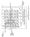
- FIG. 1 is a schematic view of a semiconductor integrated circuit device according to an embodiment of the present invention.
- reference numeral 1 represents a gate array type LSI.
- LSI 1 includes a plurality of basic gate cells 2 arranged in a matrix and a test circuit.
- the test circuit is constituted by a plurality of row selection wires 3, a plurality of column read-out wires 4, a plurality of switches 5, a row selection ring counter 6, a column selection ring counter 7, and a data selector 8.
- Each of the gate cells is constituted by, for example, a transistor-transistor logic (TTL) NAND circuit, as shown in Fig. 7. They are connected by wirings DW to constitute a logic circuit based on customer requirements, for example, as shown in Fig. 1.
- the data is input to the "INPUT" terminal, and a logic output is obtained from the "OUTPUT" terminal.
- TTL transistor-transistor logic
- Each row selection wire 3 is provided along the gate cells in the row direction, and each column read-out wire 4 is provided along the gate cells in the column direction.
- a switch 5 is provided at each intersection of the wires 3 and 4, so that the output of the corresponding gate cell 2 is connected to a column read-out wire 4 through the switch 5.
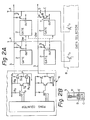
- the detailed structure of the switch 5 is shown in Fig. 2A.
- the row selection ring counter 6 is provided in order to sequentially select the row selection wires 3.
- a row selection clock is input to the input terminal 9.
- the column selection ring counter 7 is provided in order to sequentially select column read-out wires 4.
- the column selection clock is input to the input terminal 10.
- the column selection ring counter 7 and the data selector 8 constitute an output means.
- the data selector 8 is a kind of multiplexer and is constituted by a plurality of switch circuits SW, as shown in detail in Fig. 3.
- a column read-out wire 4 is selected by the column selection ring counter 7 and the selected switch circuit SW in the data selector 8 is turned on. Accordingly, the data of the selected gate cell 2 is output to the monitor output terminal 11 through the switch 5 at the intersection and the switch circuit SW in the data selector 8.
- the input terminal pin 9 is provided to the ring counter 6 for inputting the row selection clock
- the input terminal pin 10 to the ring counter 7 for inputting the column selection clock
- the monitor output terminal pin 11 to the data selector 8 for outputting the read-out data.
- a master bulk is produced in advance so as to shorten the real production time from receiving the customer's logic data to producing the final device and to reduce the real production cost. Further, some part of the mask pattern of the wiring is also fixed in advance. Only the remaining part of the wiring mask pattern is altered based on the customer's design data (logic data).
- the designed portion is just the wiring patterns DW which connect the basic gate cells 2 so as to constitute the logic circuit.
- This designed portion is the above remaining part of the wiring mask pattern.
- the other portion including the test circuits is prepared before designing the designed wirings DW.
- these prepared test circuits are constructed so as to be used after producing the actual device in which the designed wirings DW of the customer's logic data are formed on the prepared bulk.
- all outputs of the row selection ring counter 6 are low level (non-selection level). Therefore, all switches 5 are turned OFF so as not to influence the operation of the logic circuit.
- the row and column selection means which corresponds to the row and column selection ring counter, has functions of the test mode and non-test mode, which modes are selectively switched.
- test circuit The operation of the test circuit will be explained below.
- a row selection wire 3 is selected corresponding to the output of the ring counter 6 which has become a high level "1". Accordingly, row selection wires 3 are sequentially selected by the output "1" of the ring counter 6.
- all switches 5 connected to the row selection wire 3 are turned ON.
- the output data of the gate cell 2 appears on the column read-out wire 4.
- the column selection ring counter 7 selects one of the column read-out wires 4.
- the corresponding switch circuit SW in the data selector 8 is turned ON when an output of the ring counter 7 becomes a high level "1".
- the output data of the gate cell 2 is output to the monitor output terminal 11 through the selected column read-out wire 4.
- FIG. 2A shows in detail the circuit of switches 5 and an output stage of the row selection ring counter 6.
- a switch 5 is constituted by two elements, for example, an n-p-n transistor T and a resistor R.
- the resistor R is connected between a row selection wire 3 and the base of the transistor T.
- the emitter E of the transistor T is connected to the output of the gate cell 2 and the collector C is connected to a column read-out wire 4.
- the resistor R is formed by extending the base diffusion area B of the transistor T.
- the switch 5 is actually constituted by one element.
- E represents an emitter area
- B a base area
- C a collector area.
- the output stage of the row selection ring counter 6 includes transistors (T 1 , T 2 , T , and T b ), resistors (R 1 to R 4 ), and a diode D 1 .
- the transistors Ta and Tb are Schottky barrier transistors.
- An output stage is provided for every row selection wire 3. When the transistor T 1 is turned ON, the output point P becomes a high level "1" and the row selection wire 3 becomes selected. When the transistor T 2 is turned ON, the output point P becomes a low level "0" and the row selection wire 3 becomes non-selected.
- the transistor T When the row selection wire 3 becomes non-selected, i.e., low level, the transistor T is turned OFF in spite of the output level of the gate cell 2. On the other hand, when the row selection wire 3 becomes selected, i.e., high level, the base of the transistor T in the switch 5 becomes high and the transistor T is turned ON or OFF according to the output level of the gate cell 2. Accordingly, the output data of the gate cell 2 appears on the column read-out wire 4 through the transistor T.
- FIG. 3 shows in detail the switching circuits SW of the data selector 8.
- a switching circuit SW is provided at the end of each column read-out wire 4.
- Each switching circuit SW is constituted by two tran- sistors T 3 , T 4 and two resistors. All collectors of the transistors T 3 are connected to the input terminal IN of an output buffer 13 through a common data wire 12.
- the transistor T 4 is connected between the base of the transistor T 3 and the output terminal 14 of the ring counter 7.
- the transistors T 3 , T 4 of switching circuit SW constitute a NAND gate circuit with the transistor T of the switch 5. When the output terminal 14 is low (non-selected state), the transistor T 4 is turned ON and the transistor T 3 is turned OFF. When the output terminal 14 is high (selected state), the transistor T 4 is turned OFF and the transistor T 3 is turned ON or
- the transistor T 3 is turned ON. Conversely, when the output of the gate cell 2 is low, the transistor T 3 is turned OFF. Accordingly, when the transistor T 3 is turned ON, a low level signal appears on the data wire 12. When the transistor T 3 is turned OFF, a high level signal appears on the data wire 12.
- the output buffer 13 outputs a low or high level signal from the monitor output 11 corresponding to the high or low level of the data wire 12.
- the operation of the logic circuit 1 shown in Fig. 1 can be checked by the output of the monitor terminal 11. That is, the output of the gate cell 2 at each intersection is sequentially checked to see if it is the expected value (designed value). If it is, the logic circuit of the previous stage of the checked gate cell is correctly operating. Accordingly, the entire logic circuit 1 can be tested by checking sequentially each output of the gate cell 2 at the monitor terminal 11. Also, if both the selection ring counters 6 and 7 are fixed, a specific gate cell output can be monitored during the logic circuit operation so that the logic level of the predetermined point of the entire logic circuit can be monitored in real time.
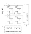
- FIG. 4 shows detailed circuits of the switch and the row selection ring counter 6 according to another embodiment.
- the switch 5 is constituted by one element, i.e., a metal-oxide semiconductor (MOS) type transistor Q.
- MOS metal-oxide semiconductor
- Each output stage of the row selection ring counter 6 is constituted by a complementary MOS (CMOS) type inverter having MOS transistors Q 1 and Q 2 instead of the two transistors T 1 , T 2 and the diode D 1 and the resistor R 1 shown in Fig. 2A.
- CMOS complementary MOS
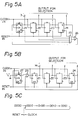
- Figures 5A and 5B show in detail the circuits of the row and column selection ring counters 6 and 7.
- reference numerals 21 to 24 represent D type flip-flop circuits, 25 an AND gate, and 26 an OR gate.
- the D type flip-flop circuits 21 to 24 are connected in series through the Q outputs.
- the Q outputs correspond to the outputs of the output stages cf the ring counter 6 or 7 shown in Figs. 2A and 4.
- the selection of the row or the selection of the column is performed according to the high or low level of the Q outputs.
- the data of the Q output of the final-stage flip-flop circuit 24 is fed back to the D input of the first-stage flip-flop circuit through the OR gate 26.
- Inverted data of the Q outputs (Q) are also input to the D input of the flip-flop circuit 21 through the AND gate 25 and the OR gate 26.
- These flip-flop circuits 21 to 24 are driven by a common clock signal (reset signal mentioned above) input to each of the CK terminals in the flip-flop circuits.
- the ring counter becomes "0" whenever the reset signal is input and restarts from the output "1,0,0,0” by the next clock signal.
- the output of the ring counter circulates between "1,0,0,0” and "0,0,0,1” until the next reset signal is input.
- the condition in which all Q outputs become the "0" state means a non-test mode, which does not affect the normal logic function of the gate array logic circuit.
- the condition in which any one of the Q outputs is the "1" state means a test mode which selects one of the row selection wire or column read-out wire.
- Figure 5B shows another embodiment of the ring counter.
- the flip-flop circuit 27 is provided at the input portion to generate "1" instead of the AND gate 25.
- all Q outputs of the flip-flop circuits 21 to 24 are set to “0" by the reset signal.
- the flip-flop circuit 27 is preset to "1". This preset signal "1" is applied to the D input of the flip-flop circuit 21 through the OR gate 26.
- the Q output of the flip-flop 27 returns to "0" by the D input level, which is fixed to low level “L”. The same operation as explained in Fig. 5A is performed until the next reset signal is input.
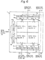
- FIG. 6 is a schematic view of a semiconductor integrated circuit device according to another embodiment of the present invention.
- all gate cells 2 are divided into, for example, four blocks 1 to 4.
- a row selection ring counter (ROW CTR I) 6a is provided for the upper half portion and the row selection ring counter (ROW CTR II) 6b for the lower half portion.
- a column selection ring counter and data selector are provided for each of blocks 1 to 4.
- a column selection ring counter (COLUMN CTR 1) 7a and data selector (SEL 1) 8a are provided for the block 1, a column selection ring counter (COLUMN CTR 2) 7b and data selector (SEL 2) 8b for block 2, a column selection ring counter (COLUMN CTR 3) 7c and data selector (SEL 3) 8c for block 3, and a column selection ring counter (COLUMN CTR 4) 7d and data selector (SEL 4) 8d for block 4.
- the necessary time for scanning all gate cells is shortened to a quarter compared with the first embodiment shown in Fig. 1, because the number of clocks for the row and column selection is reduced to half.
- three external output pins are added for each monitor output. The added monitor output pins are shown by reference numerals 31 to 33.
- the output means can be replaced with a shift register which has the same number of bits as the number of column read-out wires. That is, a parallel- in/serial-out type shift register may be used for such a register instead of the column selection ring counter and the data selector. In this case, the sequential monitor output can be obtained from the shift register.
- Figure 7 shows in detail the circuit of the gate cell 2.
- This circuit is a typical three-input TTL-NAND gate circuit.
- TR l is a multiemitter transistor. A low or high input signal is input to each of the emitters.
- TR 2 is a phase splitter transistor, and TR 4 and TR 5 are output transistors. A Darlington connection is formed by the transistors TR 3 and TR 4 .
- the test circuit does not substantially affect the logic circuit, because the test circuit is turned OFF when no gate cells are selected for checking. Moreover, it is very easy to design the logic circuit because only a switch needs to be added to each gate cell.
Landscapes
- Physics & Mathematics (AREA)
- General Physics & Mathematics (AREA)
- Engineering & Computer Science (AREA)
- General Engineering & Computer Science (AREA)
- Design And Manufacture Of Integrated Circuits (AREA)
- Semiconductor Integrated Circuits (AREA)
- Testing Or Measuring Of Semiconductors Or The Like (AREA)
- Tests Of Electronic Circuits (AREA)
Applications Claiming Priority (2)
| Application Number | Priority Date | Filing Date | Title |
|---|---|---|---|
| JP59165449A JPH073865B2 (ja) | 1984-08-07 | 1984-08-07 | 半導体集積回路及び半導体集積回路の試験方法 |
| JP165449/84 | 1984-08-07 |
Publications (2)
| Publication Number | Publication Date |
|---|---|
| EP0174236A1 true EP0174236A1 (de) | 1986-03-12 |
| EP0174236B1 EP0174236B1 (de) | 1989-07-19 |
Family
ID=15812631
Family Applications (1)
| Application Number | Title | Priority Date | Filing Date |
|---|---|---|---|
| EP85401583A Expired EP0174236B1 (de) | 1984-08-07 | 1985-08-02 | Integrierte Halbleiterschaltung mit einer Prüfschaltung |
Country Status (5)
| Country | Link |
|---|---|
| US (1) | US5764654A (de) |
| EP (1) | EP0174236B1 (de) |
| JP (1) | JPH073865B2 (de) |
| KR (1) | KR900004887B1 (de) |
| DE (1) | DE3571700D1 (de) |
Cited By (10)
| Publication number | Priority date | Publication date | Assignee | Title |
|---|---|---|---|---|
| EP0307503A1 (de) * | 1986-03-10 | 1989-03-22 | Cross-Check Technology, Inc. | Gitterförmige "querüberprüfende" Teststruktur zum Prüfen von integrierten Schaltungen |
| US5065090A (en) * | 1988-07-13 | 1991-11-12 | Cross-Check Technology, Inc. | Method for testing integrated circuits having a grid-based, "cross-check" te |
| EP0422912A3 (en) * | 1989-10-13 | 1992-05-27 | Fujitsu Limited | Semiconductor integrated circuit device having test circuit |
| EP0422930A3 (en) * | 1989-10-13 | 1992-05-27 | Fujitsu Limited | Improved cicuit arrangement of semiconductor integrated circuit device |
| EP0469809A3 (en) * | 1990-07-30 | 1992-07-01 | Fujitsu Limited | Integrated circuit arrangement suitable for testing cells arranged in rows and columns |
| EP0396660A4 (en) * | 1988-09-09 | 1992-08-05 | Cross-Check Systems, Inc. | Method and apparatus for sensing defects in integrated circuit elements |
| EP0448263A3 (en) * | 1990-03-20 | 1992-09-30 | Fujitsu Limited | Semiconductor integrated circuit device having a test circuit |
| WO1996013731A1 (en) * | 1994-10-27 | 1996-05-09 | Mitel Corporation | Semiconductor test chip with on-wafer switching matrix |
| US5799021A (en) * | 1994-10-28 | 1998-08-25 | Duet Technologies, Inc. | Method for direct access test of embedded cells and customization logic |
| CN112214964A (zh) * | 2020-12-10 | 2021-01-12 | 南京集成电路设计服务产业创新中心有限公司 | 一种动态改变布局方法、电子设备及计算机可读存储介质 |
Families Citing this family (10)
| Publication number | Priority date | Publication date | Assignee | Title |
|---|---|---|---|---|
| US4739250A (en) * | 1985-11-20 | 1988-04-19 | Fujitsu Limited | Semiconductor integrated circuit device with test circuit |
| DE3853860D1 (de) * | 1987-09-22 | 1995-06-29 | Siemens Ag | Vorrichtung zur Herstellung einer testkompatiblen, weitgehend fehlertoleranten Konfiguration von redundant implementierten systolischen VLSI-Systemen. |
| JP2673888B2 (ja) * | 1988-01-11 | 1997-11-05 | クロスチェック・テクノロジイ・インコーポレーテッド | 集積回路を電気的に試験する方法および装置 |
| JPH077079A (ja) * | 1993-06-21 | 1995-01-10 | Fujitsu Ltd | 半導体集積回路及び半導体集積回路の試験方法 |
| JPH0921848A (ja) * | 1995-07-07 | 1997-01-21 | Nec Corp | 集積回路の内部信号の観測方式 |
| US7370257B2 (en) * | 2005-04-08 | 2008-05-06 | Lsi Logic Corporation | Test vehicle data analysis |
| US7405585B2 (en) * | 2006-02-14 | 2008-07-29 | Taiwan Semiconductor Manufacturing Co., Ltd. | Versatile semiconductor test structure array |
| KR100759688B1 (ko) * | 2006-04-07 | 2007-09-17 | 삼성에스디아이 주식회사 | 원장단위 검사가 가능한 유기전계발광 표시장치 및모기판과 그 검사방법 |
| KR100871696B1 (ko) * | 2007-01-08 | 2008-12-05 | 삼성전자주식회사 | 메모리 진단 테스트 회로 및 그 테스트 방법 |
| JP5700900B2 (ja) * | 2007-04-05 | 2015-04-15 | ピーエスフォー ルクスコ エスエイアールエルPS4 Luxco S.a.r.l. | 半導体集積回路 |
Citations (2)
| Publication number | Priority date | Publication date | Assignee | Title |
|---|---|---|---|---|
| EP0073946A2 (de) * | 1981-09-07 | 1983-03-16 | Siemens Aktiengesellschaft | Verfahren und Anordnung zur Funktionsprüfung einer programmierbaren Logikanordnung |
| EP0118704A1 (de) * | 1983-02-04 | 1984-09-19 | Hitachi, Ltd. | Integrierter Schaltkreis und Methode zu seiner Prüfung |
Family Cites Families (19)
| Publication number | Priority date | Publication date | Assignee | Title |
|---|---|---|---|---|
| US3615464A (en) * | 1968-11-19 | 1971-10-26 | Ibm | Process of producing an array of integrated circuits on semiconductor substrate |
| US3893088A (en) * | 1971-07-19 | 1975-07-01 | Texas Instruments Inc | Random access memory shift register system |
| JPS4832490A (de) * | 1971-09-01 | 1973-04-28 | ||
| US3795859A (en) * | 1972-07-03 | 1974-03-05 | Ibm | Method and apparatus for determining the electrical characteristics of a memory cell having field effect transistors |
| FR2330014A1 (fr) * | 1973-05-11 | 1977-05-27 | Ibm France | Procede de test de bloc de circuits logiques integres et blocs en faisant application |
| US3958110A (en) * | 1974-12-18 | 1976-05-18 | Ibm Corporation | Logic array with testing circuitry |
| US3961252A (en) * | 1974-12-20 | 1976-06-01 | International Business Machines Corporation | Testing embedded arrays |
| US4034356A (en) * | 1975-12-03 | 1977-07-05 | Ibm Corporation | Reconfigurable logic array |
| US4196389A (en) * | 1978-07-13 | 1980-04-01 | International Business Machines Corporation | Test site for a charged coupled device (CCD) array |
| US4192016A (en) * | 1978-10-20 | 1980-03-04 | Harris Semiconductor | CMOS-bipolar EAROM |
| DE3009945C2 (de) * | 1979-03-15 | 1987-03-19 | Nippon Electric Co., Ltd., Tokio/Tokyo | Funktionsprüfbarer, integrierter Schaltkreis |
| JPS5693189A (en) * | 1979-12-18 | 1981-07-28 | Fujitsu Ltd | Field programable element |
| JPS58169937A (ja) * | 1982-03-31 | 1983-10-06 | Hitachi Ltd | 半導体集積回路装置 |
| US4490812A (en) * | 1982-09-30 | 1984-12-25 | Mostek Corporation | User reprogrammable programmed logic array |
| US4525714A (en) * | 1982-12-03 | 1985-06-25 | Honeywell Information Systems Inc. | Programmable logic array with test capability in the unprogrammed state |
| US4594711A (en) * | 1983-11-10 | 1986-06-10 | Texas Instruments Incorporated | Universal testing circuit and method |
| US4601033A (en) * | 1984-01-16 | 1986-07-15 | Siemens Corporate Research & Suppport, Inc. | Circuit testing apparatus employing signature analysis |
| US4749947A (en) * | 1986-03-10 | 1988-06-07 | Cross-Check Systems, Inc. | Grid-based, "cross-check" test structure for testing integrated circuits |
| SE516023C2 (sv) * | 1999-06-24 | 2001-11-12 | Abb Ab | Industrirobot innefattande en växellådskonfiguration samt förfarande i en industrirobot |
-
1984
- 1984-08-07 JP JP59165449A patent/JPH073865B2/ja not_active Expired - Lifetime
-
1985
- 1985-08-02 DE DE8585401583T patent/DE3571700D1/de not_active Expired
- 1985-08-02 EP EP85401583A patent/EP0174236B1/de not_active Expired
- 1985-08-07 KR KR1019850005702A patent/KR900004887B1/ko not_active Expired
-
1993
- 1993-07-12 US US08/089,635 patent/US5764654A/en not_active Expired - Fee Related
Patent Citations (2)
| Publication number | Priority date | Publication date | Assignee | Title |
|---|---|---|---|---|
| EP0073946A2 (de) * | 1981-09-07 | 1983-03-16 | Siemens Aktiengesellschaft | Verfahren und Anordnung zur Funktionsprüfung einer programmierbaren Logikanordnung |
| EP0118704A1 (de) * | 1983-02-04 | 1984-09-19 | Hitachi, Ltd. | Integrierter Schaltkreis und Methode zu seiner Prüfung |
Non-Patent Citations (2)
| Title |
|---|
| IBM TECHNICAL DISCLOSURE BULLETIN, vol. 18, no. 7, December 1975, pages 2181-2182, New York, US; D.K. JADUS et al.: "Test pad multiplexing" * |
| IEEE TRANSACTIONS ON CIRCUITS & SYSTEMS, vol. CAS-28, no. 11, November 1981, pages 1027-1032, IEEE, New York, US; H. FUJIWARA et al.: "A design of programmable logic arrays with universal tests" * |
Cited By (16)
| Publication number | Priority date | Publication date | Assignee | Title |
|---|---|---|---|---|
| EP0307503A1 (de) * | 1986-03-10 | 1989-03-22 | Cross-Check Technology, Inc. | Gitterförmige "querüberprüfende" Teststruktur zum Prüfen von integrierten Schaltungen |
| US5065090A (en) * | 1988-07-13 | 1991-11-12 | Cross-Check Technology, Inc. | Method for testing integrated circuits having a grid-based, "cross-check" te |
| EP0396660A4 (en) * | 1988-09-09 | 1992-08-05 | Cross-Check Systems, Inc. | Method and apparatus for sensing defects in integrated circuit elements |
| EP0422912A3 (en) * | 1989-10-13 | 1992-05-27 | Fujitsu Limited | Semiconductor integrated circuit device having test circuit |
| EP0422930A3 (en) * | 1989-10-13 | 1992-05-27 | Fujitsu Limited | Improved cicuit arrangement of semiconductor integrated circuit device |
| US5369646A (en) * | 1989-10-13 | 1994-11-29 | Fujitsu Limited | Semiconductor integrated circuit device having test circuit |
| EP0448263A3 (en) * | 1990-03-20 | 1992-09-30 | Fujitsu Limited | Semiconductor integrated circuit device having a test circuit |
| US5231345A (en) * | 1990-03-20 | 1993-07-27 | Fujitsu Limited | Semiconductor integrated circuit device having a test circuit |
| US5341383A (en) * | 1990-07-30 | 1994-08-23 | Fujitsu Limited | Circuit arrangement suitable for testing cells arranged in rows and columns, semiconductor integrated circuit device having the same, and method for arranging circuit blocks on chip |
| EP0469809A3 (en) * | 1990-07-30 | 1992-07-01 | Fujitsu Limited | Integrated circuit arrangement suitable for testing cells arranged in rows and columns |
| WO1996013731A1 (en) * | 1994-10-27 | 1996-05-09 | Mitel Corporation | Semiconductor test chip with on-wafer switching matrix |
| GB2310047A (en) * | 1994-10-27 | 1997-08-13 | Mitel Corp | Semiconductor test chip with on-wafer switching matrix |
| GB2310047B (en) * | 1994-10-27 | 1999-05-19 | Mitel Corp | Semiconductor test chip with on-wafer switching matrix |
| DE19581814B4 (de) * | 1994-10-27 | 2004-07-15 | Zarlink Semiconductor Inc., City Of Ottawa | Halbleiter-Testchip mit waferintegrierter Schaltmatrix |
| US5799021A (en) * | 1994-10-28 | 1998-08-25 | Duet Technologies, Inc. | Method for direct access test of embedded cells and customization logic |
| CN112214964A (zh) * | 2020-12-10 | 2021-01-12 | 南京集成电路设计服务产业创新中心有限公司 | 一种动态改变布局方法、电子设备及计算机可读存储介质 |
Also Published As
| Publication number | Publication date |
|---|---|
| KR860002147A (ko) | 1986-03-26 |
| KR900004887B1 (ko) | 1990-07-09 |
| EP0174236B1 (de) | 1989-07-19 |
| JPH073865B2 (ja) | 1995-01-18 |
| JPS6142934A (ja) | 1986-03-01 |
| DE3571700D1 (en) | 1989-08-24 |
| US5764654A (en) | 1998-06-09 |
Similar Documents
| Publication | Publication Date | Title |
|---|---|---|
| EP0174236B1 (de) | Integrierte Halbleiterschaltung mit einer Prüfschaltung | |
| US6065141A (en) | Self-diagnosable semiconductor memory device having a redundant circuit and semiconductor apparatus having the same in which the memory device cannot be accessed from outside the semiconductor apparatus | |
| US4739250A (en) | Semiconductor integrated circuit device with test circuit | |
| KR0155180B1 (ko) | 일치 검출 회로를 갖는 반도체 메모리 디바이스 및 그 테스트 방법 | |
| EP0118704B1 (de) | Integrierter Schaltkreis und Methode zu seiner Prüfung | |
| CA2092333C (en) | Built-in self-test control network | |
| US5077740A (en) | Logic circuit having normal input/output data paths disabled when test data is transferred during macrocell testing | |
| EP0398816B1 (de) | Testmethode, Testschaltung und integrierter Halbleiterschaltkreis mit Testschaltung | |
| US5369646A (en) | Semiconductor integrated circuit device having test circuit | |
| EP1224481B1 (de) | Vorrichtung und verfahren zur programierbaren parametrischen kippprüfung einer cmos digital-leitung | |
| JP3229359B2 (ja) | 集積回路を試験するための回路装置 | |
| US4581740A (en) | Transfer circuit for defect inspection of an integrated circuit | |
| JPH06102327A (ja) | メモリ内蔵型半導体集積回路およびその論理設計方法 | |
| US5363381A (en) | Integrated circuit device having macro isolation test function | |
| JPH077079A (ja) | 半導体集積回路及び半導体集積回路の試験方法 | |
| JP2594419B2 (ja) | 半導体集積回路及び半導体集積回路の試験方法 | |
| EP0422930A2 (de) | Integrierte Halbleiter-Schaltungs-Vorrichtungen | |
| EP0292116A2 (de) | Prüfsystem für VLSI-Schaltungen | |
| KR960005897Y1 (ko) | 논리소자 집적회로 | |
| JP3182442B2 (ja) | 論理集積回路 | |
| JPH0626234B2 (ja) | 半導体集積回路装置 | |
| CN118465500A (zh) | 芯片测试装置及存储介质 | |
| JPH05243969A (ja) | 半導体集積回路装置 | |
| JPH08213895A (ja) | 信号タイミング調整回路 | |
| JPH01134281A (ja) | ゲートアレイ |
Legal Events
| Date | Code | Title | Description |
|---|---|---|---|
| PUAI | Public reference made under article 153(3) epc to a published international application that has entered the european phase |
Free format text: ORIGINAL CODE: 0009012 |
|
| AK | Designated contracting states |
Kind code of ref document: A1 Designated state(s): DE FR GB |
|
| 17P | Request for examination filed |
Effective date: 19860609 |
|
| 17Q | First examination report despatched |
Effective date: 19880513 |
|
| GRAA | (expected) grant |
Free format text: ORIGINAL CODE: 0009210 |
|
| AK | Designated contracting states |
Kind code of ref document: B1 Designated state(s): DE FR GB |
|
| REF | Corresponds to: |
Ref document number: 3571700 Country of ref document: DE Date of ref document: 19890824 |
|
| ET | Fr: translation filed | ||
| PLBI | Opposition filed |
Free format text: ORIGINAL CODE: 0009260 |
|
| PLAB | Opposition data, opponent's data or that of the opponent's representative modified |
Free format text: ORIGINAL CODE: 0009299OPPO |
|
| 26 | Opposition filed |
Opponent name: CROSSCHECK TECHNOLOGY, INC. Effective date: 19900412 |
|
| R26 | Opposition filed (corrected) |
Opponent name: CROSSCHECK TECHNOLOGY, INC. Effective date: 19900412 |
|
| PGFP | Annual fee paid to national office [announced via postgrant information from national office to epo] |
Ref country code: GB Payment date: 19980724 Year of fee payment: 14 |
|
| PGFP | Annual fee paid to national office [announced via postgrant information from national office to epo] |
Ref country code: DE Payment date: 19980810 Year of fee payment: 14 |
|
| APAC | Appeal dossier modified |
Free format text: ORIGINAL CODE: EPIDOS NOAPO |
|
| RDAG | Patent revoked |
Free format text: ORIGINAL CODE: 0009271 |
|
| STAA | Information on the status of an ep patent application or granted ep patent |
Free format text: STATUS: PATENT REVOKED |
|
| 27W | Patent revoked |
Effective date: 19981105 |
|
| GBPR | Gb: patent revoked under art. 102 of the ep convention designating the uk as contracting state |
Free format text: 981105 |
|
| PGFP | Annual fee paid to national office [announced via postgrant information from national office to epo] |
Ref country code: FR Payment date: 19990810 Year of fee payment: 15 |
|
| APAH | Appeal reference modified |
Free format text: ORIGINAL CODE: EPIDOSCREFNO |