EP0175351A2 - Dispositif de lasers à semi-conducteur couplés - Google Patents
Dispositif de lasers à semi-conducteur couplés Download PDFInfo
- Publication number
- EP0175351A2 EP0175351A2 EP85111759A EP85111759A EP0175351A2 EP 0175351 A2 EP0175351 A2 EP 0175351A2 EP 85111759 A EP85111759 A EP 85111759A EP 85111759 A EP85111759 A EP 85111759A EP 0175351 A2 EP0175351 A2 EP 0175351A2
- Authority
- EP
- European Patent Office
- Prior art keywords
- laser
- middle layer
- zone
- arrangement
- layer
- Prior art date
- Legal status (The legal status is an assumption and is not a legal conclusion. Google has not performed a legal analysis and makes no representation as to the accuracy of the status listed.)
- Withdrawn
Links
Images
Classifications
-
- H—ELECTRICITY
- H01—ELECTRIC ELEMENTS
- H01S—DEVICES USING THE PROCESS OF LIGHT AMPLIFICATION BY STIMULATED EMISSION OF RADIATION [LASER] TO AMPLIFY OR GENERATE LIGHT; DEVICES USING STIMULATED EMISSION OF ELECTROMAGNETIC RADIATION IN WAVE RANGES OTHER THAN OPTICAL
- H01S5/00—Semiconductor lasers
- H01S5/40—Arrangement of two or more semiconductor lasers, not provided for in groups H01S5/02 - H01S5/30
- H01S5/4025—Array arrangements, e.g. constituted by discrete laser diodes or laser bar
- H01S5/4031—Edge-emitting structures
- H01S5/4043—Edge-emitting structures with vertically stacked active layers
Definitions
- the present invention relates to a coupled laser diode arrangement, as specified in the preamble of claim 1.
- Such a wave mechanical coupling is used, for example, to generate single-mode laser radiation. It can also be used to control the laser radiation generation in one zone by changing the intensity and / or changing the excitation conditions of the laser radiation in the other adjacent zone.
- pp. 619-622 arrangements are known which have a first and a second zone lying one above the other. Although laser radiation runs in both zones, radiation is generated by current flow through a pn junction of the layer structure only in the first zone.
- the other second zone is a passive optical resonator which is mechanically coupled to the first zone containing the pn junction.
- the effective band gap in the material of this second zone ie in the zone of the passive resonator, is greater than that in the first zone with the pn junction. If laser radiation were generated in this second zone, its frequency would be different from, namely be higher than the frequency of the laser radiation that is actually generated in this known arrangement in its first zone with a pn junction. However, this would make the proposed wave mechanical coupling impossible, ie the passive property of this second zone is of crucial importance for this prior art.
- the laser diodes are generally those of the double heterostructure type, for example made of indium gallium arsenide phosphide / indium phosphide.
- two laser diodes to be coupled to one another can also be arranged at a short distance from one another, even if they are designed as index-guided laser diodes.
- the object of the present invention is to provide an arrangement and a production method for this arrangement in which reduced technological effort and / or increased security for maintaining predetermined distances is achieved.
- the principle of the solution according to the invention is to arrange two or more strip-shaped laser-active zones adjacent to one another, one above the other, in the entire semiconductor body.
- the semiconductor bodies of the laser diodes and in particular those with a double heterostructure are made up of multiple epi tactical deposition of different layers on top of each other.
- Three layers and a substrate body are generally required for a double heterostructure, the substrate body also being able to take on the function of one of the layers.
- the laser-active zone is at least largely in the area of the middle layer (in the case of a 3-layer arrangement), the very precise location of known technological subtleties such as the degree of doping and, if appropriate, gradient and / or the choice of materials of the layer sequence and the like. depends.
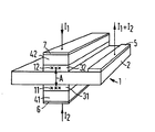
- 1 designates the entire arrangement consisting of two coupled strip-shaped laser-active zones with two coupled laser diodes.
- one of the laser diodes coupled to one another is arranged above and below the portion 2 serving as substrate body, for example in P ...
- the substrate body is the middle layer 2 and also the first layer of the respective double heterostructure of the individual diodes, to which the layers 31 and 32 as well as 41 and 42 belong. There are therefore two parts of symmetry.
- these layers 31, 32, 41, 42 are epitaxially deposited one on top of the other or on the middle layer 2.
- the shape shown in the figure will be produced by a subsequent etching process, since shaping of this type is possible in the course of epitaxial deposition, but is complex.
- the layers 31, 2 consist, for example, of In GaAs P and the layers 41 and 42 consist of, for example, In P.
- the electrical substrate connection for example a streak fen-shaped contact electrode.
- Further strip-shaped or sheet-like ecle electrodes are designated by 6 and 7.
- the electrical current I 1 , 1 2 used for laser excitation flows, for example, as indicated in the figure.
- the end cross-sectional areas of the respective strip-shaped laser-active zone are designated by 11 and 12.
- the distance A is indicated by the arrow A.
- the substrate 2 is an essential part of the semiconductor material located between the zones 11 and 12, via which the wave-optical coupling takes place.
- the thickness of this middle layer 2 for which dimensions of approximately 0.1 to 0.3 ⁇ m are to be observed, essentially determines the distance A.
- the thickness of a layer can be set or maintained very precisely.
- the invention also offers the guarantee of low copy scatter and low rejects for mass production.
- the invention also has the advantage that (later) external influences which act on the arrangement 1 cannot act on the distance-dependent wave-optical coupling of the zones 11 and 12.
- the coupling area is hermetically sealed from the outside.
- An arrangement 1 according to the invention is produced by epitaxially depositing the layer sequence to be seen from the figure, and advantageously subsequently etching away the semiconductor components initially formed laterally on the layers 41, 31, 32 and 42. This is done with commonly used mask etching, ion beam etching and the like.
Landscapes
- Physics & Mathematics (AREA)
- Condensed Matter Physics & Semiconductors (AREA)
- General Physics & Mathematics (AREA)
- Electromagnetism (AREA)
- Optics & Photonics (AREA)
- Semiconductor Lasers (AREA)
Applications Claiming Priority (2)
| Application Number | Priority Date | Filing Date | Title |
|---|---|---|---|
| DE3434741 | 1984-09-21 | ||
| DE19843434741 DE3434741A1 (de) | 1984-09-21 | 1984-09-21 | Verkoppelte laserdioden-anordnung |
Publications (2)
| Publication Number | Publication Date |
|---|---|
| EP0175351A2 true EP0175351A2 (fr) | 1986-03-26 |
| EP0175351A3 EP0175351A3 (fr) | 1987-07-29 |
Family
ID=6246018
Family Applications (1)
| Application Number | Title | Priority Date | Filing Date |
|---|---|---|---|
| EP85111759A Withdrawn EP0175351A3 (fr) | 1984-09-21 | 1985-09-17 | Dispositif de lasers à semi-conducteur couplés |
Country Status (4)
| Country | Link |
|---|---|
| US (1) | US4742525A (fr) |
| EP (1) | EP0175351A3 (fr) |
| JP (1) | JPS6179287A (fr) |
| DE (1) | DE3434741A1 (fr) |
Families Citing this family (9)
| Publication number | Priority date | Publication date | Assignee | Title |
|---|---|---|---|---|
| DE3708666C2 (de) * | 1987-03-17 | 1997-11-27 | Siemens Ag | Laseranordnung mit getrennt ansteuerbaren gekoppelten Halbleiterlasern |
| EP0360011B1 (fr) * | 1988-09-22 | 1994-02-16 | Siemens Aktiengesellschaft | Laser DFB accordable |
| US4987576A (en) * | 1988-11-30 | 1991-01-22 | Siemens Aktiengesellschaft | Electrically tunable semiconductor laser with ridge waveguide |
| JPH07112096B2 (ja) * | 1990-11-14 | 1995-11-29 | 光計測技術開発株式会社 | 半導体素子 |
| EP1014455B1 (fr) | 1997-07-25 | 2006-07-12 | Nichia Corporation | Dispositif a semi-conducteur en nitrure |
| JP3770014B2 (ja) | 1999-02-09 | 2006-04-26 | 日亜化学工業株式会社 | 窒化物半導体素子 |
| WO2000052796A1 (fr) | 1999-03-04 | 2000-09-08 | Nichia Corporation | Element de laser semiconducteur au nitrure |
| KR20030082281A (ko) * | 2002-04-17 | 2003-10-22 | 엘지전자 주식회사 | 이중 파장의 광을 방출하는 반도체 레이저 다이오드 및그의 제조방법 |
| TWI362769B (en) | 2008-05-09 | 2012-04-21 | Univ Nat Chiao Tung | Light emitting device and fabrication method therefor |
Family Cites Families (5)
| Publication number | Priority date | Publication date | Assignee | Title |
|---|---|---|---|---|
| GB1543405A (en) * | 1975-03-29 | 1979-04-04 | Licentia Gmbh | Method of and arrangement for producing coherent mode radiation |
| JPS5723291A (en) * | 1980-07-16 | 1982-02-06 | Sony Corp | Semiconductor laser device |
| US4347612A (en) * | 1980-08-25 | 1982-08-31 | Xerox Corporation | Semiconductor injection laser for high speed modulation |
| FR2525034A1 (fr) * | 1982-04-09 | 1983-10-14 | Carenco Alain | Laser a semiconducteur a coupleur directif permettant une sortie laterale |
| DE3477980D1 (en) * | 1983-02-25 | 1989-06-01 | American Telephone & Telegraph | Multicavity optical device and applications thereof |
-
1984
- 1984-09-21 DE DE19843434741 patent/DE3434741A1/de not_active Withdrawn
-
1985
- 1985-09-06 US US06/773,018 patent/US4742525A/en not_active Expired - Fee Related
- 1985-09-17 EP EP85111759A patent/EP0175351A3/fr not_active Withdrawn
- 1985-09-19 JP JP60207706A patent/JPS6179287A/ja active Pending
Also Published As
| Publication number | Publication date |
|---|---|
| US4742525A (en) | 1988-05-03 |
| DE3434741A1 (de) | 1986-04-03 |
| EP0175351A3 (fr) | 1987-07-29 |
| JPS6179287A (ja) | 1986-04-22 |
Similar Documents
| Publication | Publication Date | Title |
|---|---|---|
| DE4135813C2 (de) | Oberflächenemittierende Halbleiter-Laservorrichtung | |
| DE2165006C3 (de) | Halbleiterlaser | |
| DE69107428T2 (de) | Optoelektronische Vorrichtungen mit abstimmbarer Polarisation. | |
| DE19624514C1 (de) | Laserdiode-Modulator-Kombination | |
| DE69719268T2 (de) | Herstellungsverfahren einer optoelektrischen Halbleitervorrichtung, und Vorrichtung oder Matrix von Vorrichtungen hergestellt unter Verwendung dieses Verfahrens | |
| EP0672311B1 (fr) | Diode laser accordable a emission de surface | |
| DE60107679T2 (de) | Oberflächenemittierender Laser mit vertikalem Resonator auf Indiumphosphid-Basis | |
| DE3007809C2 (de) | Halbleiterlichtausstrahlungselement und Verfahren zu seiner Herstellung | |
| DE68910369T2 (de) | Phasengekoppeltes Halbleiterlaser-Array unter Verwendung nahe beieinanderliegender Wellenleiter mit negativem Brechungsindex. | |
| DE2120464B2 (de) | Heterostruktur-Halbleiterdiode mit pn-übergang zur Verwendung als Injektionslaser | |
| DE69222617T2 (de) | Nicht-lineare optische Vorrichtung | |
| DE3300986A1 (de) | Mehrschichtige optische integrierte schaltung | |
| WO2009143813A1 (fr) | Laser semiconducteur à structure de phase et à émission latérale | |
| DE2552870A1 (de) | Halbleiter-laserdiode | |
| DE2425363A1 (de) | Halbleiterinjektionslaser | |
| DE3502326A1 (de) | Licht emittierender chip und damit arbeitende optische kommunikationsvorrichtung | |
| EP0175351A2 (fr) | Dispositif de lasers à semi-conducteur couplés | |
| DE19945134C2 (de) | Lichtemittierendes Halbleiterbauelement hoher ESD-Festigkeit und Verfahren zu seiner Herstellung | |
| DE2447536C2 (de) | Halbleiterlaser | |
| DE4034187A1 (de) | Optisches halbleiterelement | |
| DE102020108941B4 (de) | Diodenlaser mit verrringerter Strahldivergenz | |
| DE3875882T2 (de) | Quantum-well-modulator fuer elektromagnetische wellen und anwendung dieses modulators als polarisator. | |
| DE69616237T2 (de) | Halbleiter-laserdiode und deren herstellungsverfahren | |
| DE3888575T2 (de) | Lichtemittierende Vorrichtung. | |
| DE3689742T2 (de) | Halbleiterlaser. |
Legal Events
| Date | Code | Title | Description |
|---|---|---|---|
| PUAI | Public reference made under article 153(3) epc to a published international application that has entered the european phase |
Free format text: ORIGINAL CODE: 0009012 |
|
| 17P | Request for examination filed |
Effective date: 19850925 |
|
| AK | Designated contracting states |
Kind code of ref document: A2 Designated state(s): DE FR GB |
|
| PUAL | Search report despatched |
Free format text: ORIGINAL CODE: 0009013 |
|
| AK | Designated contracting states |
Kind code of ref document: A3 Designated state(s): DE FR GB |
|
| 17Q | First examination report despatched |
Effective date: 19891002 |
|
| STAA | Information on the status of an ep patent application or granted ep patent |
Free format text: STATUS: THE APPLICATION HAS BEEN WITHDRAWN |
|
| 18W | Application withdrawn |
Withdrawal date: 19900131 |
|
| R18W | Application withdrawn (corrected) |
Effective date: 19900131 |
|
| RIN1 | Information on inventor provided before grant (corrected) |
Inventor name: AMANN, MARKUS-CHRISTIAN, DR. Inventor name: HEINEN, JOCHEN, DR. |