EP0175501B1 - Circuit de retard pour réseau de portes LSI - Google Patents
Circuit de retard pour réseau de portes LSI Download PDFInfo
- Publication number
- EP0175501B1 EP0175501B1 EP85306004A EP85306004A EP0175501B1 EP 0175501 B1 EP0175501 B1 EP 0175501B1 EP 85306004 A EP85306004 A EP 85306004A EP 85306004 A EP85306004 A EP 85306004A EP 0175501 B1 EP0175501 B1 EP 0175501B1
- Authority
- EP
- European Patent Office
- Prior art keywords
- channel
- inverter
- transistors
- potential
- output
- Prior art date
- Legal status (The legal status is an assumption and is not a legal conclusion. Google has not performed a legal analysis and makes no representation as to the accuracy of the status listed.)
- Expired - Lifetime
Links
Images







Classifications
-
- H—ELECTRICITY
- H03—ELECTRONIC CIRCUITRY
- H03K—PULSE TECHNIQUE
- H03K5/00—Manipulating of pulses not covered by one of the other main groups of this subclass
- H03K5/13—Arrangements having a single output and transforming input signals into pulses delivered at desired time intervals
- H03K5/133—Arrangements having a single output and transforming input signals into pulses delivered at desired time intervals using a chain of active delay devices
-
- H—ELECTRICITY
- H03—ELECTRONIC CIRCUITRY
- H03K—PULSE TECHNIQUE
- H03K5/00—Manipulating of pulses not covered by one of the other main groups of this subclass
- H03K2005/00013—Delay, i.e. output pulse is delayed after input pulse and pulse length of output pulse is dependent on pulse length of input pulse
- H03K2005/0015—Layout of the delay element
- H03K2005/00195—Layout of the delay element using FET's
- H03K2005/00215—Layout of the delay element using FET's where the conduction path of multiple FET's is in parallel or in series, all having the same gate control
Definitions
- the present invention relates to a delay circuit applied to, for example, a gate-array large-scale integrated circuit (LSI).
- LSI gate-array large-scale integrated circuit
- a delay circuit is used for delaying the propagation of a signal for a definite time period.
- Such a delay circuit must offer an optimum delay time period, a small mounting area, and minimum fluctuation of the delay time period.
- a delay time period t pd of one gate of a metal-insulator-semiconductor (MIS) transistor can be represented by t pd ⁇ C/g m where C is a load capacity, and g m is the conductance of the transistor.
- C is a load capacity
- g m is the conductance of the transistor.
- W and L are the width and length, respectively, of a gate of the transistor. Therefore, it is possible to increase the delay time period by using an inverter of MIS transistors having a small gate width W and a large gate length L.
- a gate-array LSI since only transistors having a definite size are used, it is impossible to arbitrarily change the size of the transistors. In other words, in a gate-array LSI, it is impossible to decrease the gate width W and increase the gate length L only for special transistors.
- a delay circuit by using a resistance-capacitance (RC) circuit.
- the delay time period must be adjusted by the resistance of polycrystalline silicon or the resistance of a diffusion region.
- RC resistance-capacitance
- a delay circuit comprising: an input terminal; an output terminal; first and second power supply means; and inverter circuitry comprising a plurality of transistors connected in series between the first and second power supply means and providing first and second inverters connected in series between said input terminal and said output terminal; characterised in that each of said first and second inverters comprises a number of P-channel transistors and an equal number of N-channel transistors connected in series between said first and second power supply terminals; and in that common outputs of pairs of P-channel/N-channel transistors of said second inverter are fed back to inputs of pairs of P-channel/N-channel transistors of said first inverter.
- An embodiment of the present invention can provide a delay circuit, suitable for a gate-array LSI, having a small area.
- two inverters having series-connected P-channel/N-channel transistors in which the outputs of the post-stage inverter are fed back to some of the inputs of the pre-stage inverters, are provided.
- the driving ability thereof is reduced, thereby increasing the delay time period. Also, a large fan-out is obtained.
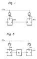
- Fig. 1 is a partial circuit diagram of a gate-array LSI having no delay circuit
- Figs. 2A, 2B, 2C, and 2D are timing diagrams showing the operation of the circuit of Fig. 1
- Fig. 3 is a partial circuit diagram of a gate-array LSI having a delay circuit
- Figs. 4A, 4B, 4C, 4D, and 4E are timing diagrams showing the operation of the circuit of Fig. 3
- Fig. 5 is a circuit diagram of a prior art delay circuit
- Fig. 6 is an equivalent circuit diagram of an example of one basic cell used in a complementary MIS gate array LSI
- Fig. 6 is an equivalent circuit diagram of an example of one basic cell used in a complementary MIS gate array LSI
- FIG. 18 is a circuit diagram of an embodiment of the delay circuit according to the present invention
- Figs. 19 and 20 are circuit diagrams for explaining the operation of Fig. 18
- Figs. 21 through 24 are timing diagrams showing the operation of the circuit of Fig. 18
- Fig. 25 is a circuit diagram of another embodiment of the delay circuit according to the present invention
- Fig. 26 is a circuit diagram of a further embodiment of the delay circuit according to the present invention
- Figs. 27 and 28 are timing diagrams for explaining the operation of Fig. 26.
- Fig. 1 is a partial circuit diagram of a gate-array LSI
- a clock signal CK0 is delayed by time periods t1 and t2 to generate clock signals CK1 and CK2 , as shown in Figs. 2A, 2B, and 2D, thereby latching flip-flops FF1 and FF2.
- the flip-flop FF1 is latched by the clock signal CK1 as shown in Fig. 2C
- a latch operation for the flip-flop FF2 by the clock signal CK2 may be performed upon the next data. This means that the hold time period of the input data of the flip-flop FF2 by the clock signal CK2 may be reduced.
- a delay circuit DL is interposed between the flip-flops FF1 and FF2 , as illustrated in Fig. 3.
- the data output Q of the flip-flop FF1 is delayed by a time period t d .
- the data input D of the flip-flop FF2 is delayed by the time period t d as compared with the data output Q of the flip-flop FF1, as shown in Figs. 4C and 4D, and the hold time period of the flip-flop FF2 by the clock signal CK2 becomes sufficiently large.
- Figure 5 shows a prior art delay circuit used in a gate-array LSI.
- a series of inverters INV are provided.
- Each of the inverters INV is constructed by a basic cell, which consists, for example, of four two-input gates.
- FIG. 6 is an equivalent circuit diagram of a complementary MIS (CMIS) basic cell.
- the basic cell is comprised of a pair of P-channel transistors Q 1p and Q 2p having a common source and a pair of N-channel transistors Q 1n and Q 2n having a common source.
- the gates of the P-channel transistor Q 1p and the N-channel transistor Q 1n are connected to each other, and the gates of the P-channel transistor Q 2p and the N-channel transistor Q 2n are connected to each other.
- Fig. 7 is a plan view of the basic cell of Fig. 6, and Figs.
- reference numeral 1 designates an N ⁇ -type monocrystalline silicon substrate 1 having a P ⁇ -type well 2 for the N-channel transistors Q 1n and Q 2n . Further, a field oxide layer 3 for isolating transistors (active areas) from each other is formed thereon, and a gate oxide layer 4 is formed on each active area. Further, P+-type impurity diffusion regions 5 are formed for the P-channel transistors Q 1p and Q 2p , and N+-type impurity diffusion regions 6 are formed for the N-channel transistors Q 1n and Q 2n .
- polycrystalline silicon layers 7 are formed for the connection of the gates of the transistors Q 1p and Q 1n and the connection of the gates of the transistors Q 2p and Q 2n , thus completing the bulk process of a gate-array LSI.
- connection patterns are formed on the basic cell as shown in Figs. 6 through 9.
- each inverter INV is constructed by a basic cell as shown in Figs. 6 through 9.
- each inverter INV uses only two gates, e.g., the transistors Q 1p and Q 1n , and does not use the other two gates, e.g., the transistors Q 2p and Q 2n .
- the delay time period of the first stage is 0.77 ns
- the delay time period of the second stage is 0.43 ns
- the delay time period of the third stage is 0.77 ns
- the delay time period of the fourth stage is 0.71 ns. Therefore, the total delay time period is 2.68 ns.
- the delay time period of the first stage is 0.43 ns; the delay time period of the second stage is 0.77 ns; the delay time period of the third stage is 0.43 ns; and the delay time of the fourth stage is 1.32 ns. Therefore, the total delay time period is 2.95 ns.
- the delay circuit of Fig. 5 requires a large number of inverters stages, i.e., basic cells, occupying a large area.
- P-channel transistors Q 1p , Q 2p , Q 3p , and Q 4p are connected in series between a power supply terminal V cc and an output terminal OUT, and N-channel transistors Q 1n , Q 2n , Q 3n , and Q 4n are connected in series between the output terminal OUT and the ground. Further, a load capacity C L is connected to the output terminal OUT.
- the P-channel transistors Q 1p , Q 2p , Q 3p , and Q 4p and the N-channel transistors Q 1n , Q 2n , Q 3n , and Q 4n are all driven by the potential at the input terminal IN.
- the transistors Q 1p , Q 2p , Q 3p , and Q 4p are in an on state, and the transistors Q 1n , Q 2n , Q 3n , and Q 4n are in an off state. Therefore, the load capacity C L is charged at V cc by the transistors Q 1p , Q 2p , Q 3p , and Q 4p , so that the potential at the output terminal OUT is high.
- the transistors Q 1n , Q 2n , Q 3n , and Q 4n are in an on state, and the transistors Q 1p , Q 2p , Q 3p , and Q 4p are in an off state. Therefore, the load capacity C L is discharged by the transistors Q 1n , Q 2n , Q 3n , and Q 4n , so that the potential at the output terminal OUT is low.
- the P-channel transistors Q 1p , Q 2p , Q 3p , and Q 4p are sequentially turned on, in that order, and the N-channel transistors Q 4n , Q 3n , Q 2n , and Q 1n are sequentially turned off, in that order, since the gate-source voltage of a P-channel transistor (N-channel transistor) on the outside is not smaller than the gate-source voltage of a P-channel transistor (N-channel transistor) on the inside.
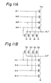
- the output terminal OUT is charged by the P-channel transistors Q 1p , Q 2p , Q 3p , and Q 4p , so that its potential rises in the same way as the rise operation in a four-input NOR circuit as shown in Fig. 11A.
- the N-channel transistors Q 1n , Q 2n , Q 3n , and Q 4n are sequentially turned on, in that order, and the P-channel transistors Q 4p , Q 3p , Q 2p , and Q 1p are sequentially turned off in that order, since, also in this case, the gate-source voltage of a P-channel transistor (N-channel transistor) on the outside is not smaller than the gate-source voltage of a P-channel transistor (N-channel transistor) on the inside.
- the output terminal OUT is discharged by the N-channel transistors Q 1n , Q 2n , Q 3n , and Q 4n , so that its potential falls in the same way as the fall operation in a four-input NAND circuit as shown in Fig. 11B.
- the P-channel transistors (or the N-channel transistors) are sequentially turned on from the outside to the inside, and the N-channel transistors (or the P-channel transistors) are turned on, the change of the potential at the output terminal OUT is delayed.
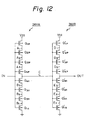
- an inverter INVA is comprised of P-channel transistors Q 1p , Q 2p , Q 3p , and Q 4p and N-channel transistors Q 1n , Q 2n , Q 3n , and Q 4n connected in series
- an inverter INVB is comprised of P-channel transistors Q 1p ' , Q 2p ' , Q 3p ' , and Q 4p ' and N-channel transistors Q 1n ' , Q 2n ' , Q 3n ' , and Q 4n ' connected in series.
- the potential at the input terminal IN is applied to the gates of the transistors Q 1p , Q 2p , Q 3p , Q 4p , Q 1n , Q 2n , Q 3n , and Q 4n of the inverter INVA. Accordingly, these transistors are driven by the potential at the input terminal IN. Also, the common output C of the innermost pair of the P-channel/N-channel transistors Q 4p and Q 4n of the inverter INVA is applied to the gates of the transistors Q 1p ', Q 2p ', Q 3p ', Q 4p ', Q 1n ', Q 2n ', Q 3n ', and Q 4n ' of the inverter INVB.
- these transistors are driven by the potential at the output C. Also, the common output of the innermost pair of the P-channel/N-channel transistors Q 4p ' and Q 4n ' of the inverter INVB is connected to the output terminal OUT.
- the transistors Q 1p , Q 2p , Q 1n , and Q 2n can be constructed by one basic cell; the transistors Q 3p , Q 4p , Q 3n , and Q 4n can be constructed by one basic cell; the transistors Q 1p ', Q 2p ', Q 1n ', and Q 2n ' can be constructed by one basic cell; and the transistors Q 3p ', Q 4p ', Q 3n ', and Q 4n ' can be constructed by one basic cell. Therefore, the circuit of Fig. 12 can be constructed by four basic cells in the same way as in the circuit of Fig. 5.
- FIG. 13 shows the case wherein the fan-out (F/O) is 0 and wherein the potential at the input terminal IN is changed from low to high
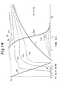
- Fig. 14 shows the case wherein the fan-out (F/O) is 0 and wherein the potential at the input terminal IN is changed from high to low
- Fig. 15 shows the case wherein the fan-out (F/O) is 5 and wherein the potential at the input terminal IN is changed from low to high
- Fig. 16 shows the case wherein the fan-out (F/O) is 5 and wherein the potential at the input terminal IN is changed from high to low.
- the P-channel transistors Q 1p , Q 2p , Q 3p , and Q 4p are in an on state, and the N-channel transistors Q 1n , Q 2n , Q 3n , and Q 4n are in an off state, and, accordingly, the potential at the node C is high.
- P-channel transistors Q1 ' p , Q2 ' p , Q3 ' p and Q4 ' p are in an off state, and the N-channel transistors Q1 ' n , Q2 ' n , Q3 ' n , and Q4 ' n are in an on state, and accordingly, the potential at the output terminal OUT is low.
- the N-channel transistors Q 1n , Q 2n , Q 3n , and Q 4n tend to be in an on state, while the transistors Q 1p , Q 2p , Q 3p , and Q 4p tend to be in an off state.
- the potentials at the nodes A1 , A2 , A3 , and C temporarily rise up to a level higher than the power supply potential V cc by the gate-source capacitance of each of the transistors Q 1P to Q 4P and Q rn . Then, as the transistors Q 1n , Q 2n , Q 3n , and Q 4n become in an on state, the node C is discharged via these transistors. As a result, the potential at the node C is reduced, and simultaneously, the potentials at the nodes B1 , B2 , and B3 change toward their DC stable points determined by the impedance ratio of the transistors.
- the transistors Q 1p ', Q 2p ', Q 3p ', and Q 4p ' tend to be in an on state, and accordingly, the potentials at the nodes D1 , D2 , and D3 change toward a DC stable point determined by the impedance ratio of the transistors Q 1p ', Q 2p ' , Q 3p ' , and Q 4p '.
- the potentials at the nodes E1 , E2 , and E3 become lower than the ground level due to the rapid reduction of the potential at the node C.
- the transistors Q 1n , Q 2n , Q 3n , and Q 4n are completely in an on state. Therefore, the potentials at the nodes C, B1 , B2 , and B3 are reduced by the discharging operation. Note that, at this time, since the transistors Q 1p , Q 2p , Q 3p , and Q 4p are completely in an off state, the potentials at the nodes E1 , E2 , and E3 become levels in accordance with the impedance determined by the leakage currents of the transistors Q 1n ', Q 2n ', Q 3n ', and Q 4n ' after a sufficient time period passes.
- the potential at the output terminal OUT is changed by the (charging and) discharging operation of the transistors Q 1p ' , Q 2p ' , Q 3p ' , and Q 4p ' and the transistors Q 1n , Q 2n , Q 3n , and Q 4n .
- a charging and discharging operation is carried out by a large number of transistors, thereby increasing the delay time period.
- a delay time period having a time larger than 5 ns can be obtained, and therefore, is larger than that of the circuit of Fig. 5.
- each of the inverters has the same number of P-channel transistors and N-channel transistors connected in series. Any number can be, of course, selected, however.
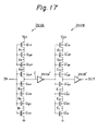
- Fig. 17 two inverters INVA' and INVB' are added to the circuit of Fig. 12. That is, the inverter INVA' is interposed between the inverters INVA and INVB, and the inverter INVB' is connected to the output of the inverter INVB.
- the inverters INVA' and INVB' serve as wave-shaping means. Each of them may be constructed by two gates of one basic cell, for example as shown in Figs. 6 through 9.
- Fig. 18 which illustrates an embodiment of the present invention, two inverters INVA and INVB are provided.
- each pair of P-channel/N-channel transistors Q 1p and Q 1n ; Q 2p and Q 2n ; Q 3p and Q 3n ; and Q 4p and Q 4n form one inverter.
- each pair of P-channel/ N-channel transistors Q 1p ' and Q 1n ' ; Q 2p ' and Q 2n '; Q 3p ' and Q 3n '; and Q 4p ' and Q 4n ' forms one inverter.
- FIG. 19 are absent in Fig. 18. They are provided in Fig. 19 only for easy understanding of the operation thereof. Further, if the inverters INV3 to INV8 were defined by transfer gates, the circuit of Fig. 18 would be as schematically illustrated in Fig. 20.
- the inverter INV1 (Q 1p , Q 1n ) is driven by the potential at the input terminal IN; the inverter INV2 (Q 1p ', Q 1n ') is driven by the output A of the inverter INV1; the inverter INV3 (Q 2p , Q 2n ) is driven by the output B of the inverter INV2; the inverter INV4 (Q 2p ', Q 2n ') is driven by the output C of the inverter INV3; the inverter INV5 (Q 3p , Q 3n ) is driven by the output D of the inverter INV4; the inverter INV6 (Q 3p ', Q 3n ') is driven by the output E of the inverter INV5; the inverter INV7 (Q 4p , Q 4n ) is driven by the output F of the inverter INV6; the inverter INV8 (Q 4p ',
- each inverter of the post-stage inverter INVB is fed back to the input of each inverter of the pre-stage inverter INVA. Accordingly, the driving power of each inverter (INV1 to INV8) is reduced, thereby increasing the delay time period.
- circuit of Fig. 18 is constructed by basic cells each having four two-input gates as shown in Figs. 6 through 9, the circuit of Fig. 18 can be constructed by four basic cells in the same way as in the circuit of Fig. 12.
- Figures 21 through 24 correspond to Figs. 13 through 16, respectively. That is, Fig. 21 shows the case wherein the fan-out (F/O) is 0 and wherein the potential at the input terminal IN is changed from low to high; Fig. 22 shows the case wherein the fan-out (F/O) is 0 and wherein the potential at the input terminal IN is changed from high to low; Fig. 23 shows the case wherein the fan-out (F/O) is 5 and wherein the potential at the input terminal IN is changed from low to high; and Fig. 24 shows the case wherein the fan-out (F/O) is 5 and wherein the potential at the input terminal IN is changed from high to low.
- the transistor Q 2p When the potential at the output B reaches the above-mentioned threshold value, the transistor Q 2p is cut off, and the discharge at the outputs C, E, and G temporarily ceases. Further, when the potential at the output B increases, the potential at the output C remains temporarily at the same level and, accordingly, the transistor Q 2n ' is cut off. As a result, only the potential at the output B increases. Therefore, the output C of the inverter INV3 (Q 2p , Q 2n ) is again reduced. At this time, since the transistors Q 3p and Q 4p are still in an on state, the potentials at the outputs E and G are also reduced.
- Fig. 21 is replaced by Fig. 23 and Fig. 22 is replaced by Fig. 24. That is, the waveform at the output terminal OUT is blunt and the delay time period is further increased.
- a delay time period having a time larger than 5 ns can be obtained and therefore, is larger than that of Fig. 5.
- Fig. 25 which illustrates another embodiment of the present invention similar to the embodiment as shown in Fig. 18, the inverters INV3 (Q 2p , Q 2n ), INV5 (Q 3p , Q 3n ), and INV7 (Q 4p , Q 4n ) of the inverter INVA are driven simultaneously by the output B of the inverter INV2 (Q 1p ', Q 1n ') of the inverter INVB, and the inverters INV4 (Q 2p ', Q 2n '), INV6 (Q 3p ', Q 3n '), and INV8 (Q 4p ', Q 4n ') of the inverter INVB are driven simultaneously by the output (C) of the inverter INV7 (Q 4p , Q 4n ) of the inverter INVA.
- the P-channel transistors Q 2p , Q 3p , and Q 4p tend to be in an on state and the N-channel transistors Q 2n , Q 3n and Q 4n tend to be in an off state, and accordingly, the high potential at the output A is transmitted to the output C. Therefore, the output C becomes high, so that the potential at the output terminal OUT becomes low. In such a configuration, unstable waveforms are hardly ever generated in the output terminal OUT as compared with the embodiment of Fig. 18.
- Fig. 26 which illustrates a further embodiment of the present invention similar to the embodiment of Fig. 25, the inverters INV3 (Q 2p , Q 2n ), INV5 (Q 3p , Q 3n ), and INV7 (Q 4p , Q 4n ) of the inverter INVA are driven by the potential at the output terminal OUT, not the output of the inverter INV2 (Q 1p ', Q 1n ') of the inverter INVB.
- Fig. 27 in an initial state, the potentials at the input terminal IN and the output terminal OUT are low. At this time, since the transistors Q 1p to Q 4p are in an on state, the potentials at the nodes A, C1 , C2 , and B are high, and accordingly, the transistors Q 1n ' to Q 4n ' are in an on state, so that the potentials at nodes F1 , F2 , and F3 are low. In this state, when the potential at the input terminal IN is changed from low to high, the potential at the output A of the inverter INV1 (Q 1p , Q 1n ) is reduced.
- the transistors Q 2p , Q 3p , and Q 4p are still in an on state, the potentials at the nodes C1 and C2 and at the node B are also decreased with the decrease of the potential A.
- the transistors Q 4p ', Q 3p ', and Q 2p ' tend to be in an on state, so that the nodes E1 , E2 , and E3 are discharged to decrease the potentials thereof.
- the potentials at the output terminal OUT and the nodes F1 , F2 , and F3 are increased.
- Such an unstable state continues until the potential at the output terminal OUT reaches the threshold value of the P-channel transistor Q 2p .
- the transistors Q 2p , Q 3p , and Q 4p are cut off to again decrease the potential at the node B.
- Fig. 28 in an initial state, the potentials at the input terminal IN and the output terminal OUT are high. At this time, since the transistors Q 1n to Q 4n are in an on state, the potentials at the nodes A, D1 , D2 , and B are low. Accordingly, the transistors Q 1p ' to Q 4p ' are in an on state, so that the potentials at nodes E1 , E2 , and E3 are high. In this state, when the potential at the input terminal IN is changed from high to low, the potential at the output A of the inverter INV1 (Q 1p , Q 1n ) is increased.
- the transistors Q 2n , Q 3n , and Q 4n are still in an on state, the potentials at the nodes D1 and D2 and at the node B are also increased with the increase of the potential A.
- the transistors Q 4n ', Q 3n ', and Q 2n ' tend to be in an on state, so that the nodes F1 , F2 , and F3 are charged to increase the potentials thereof.
- the potentials at the output terminal OUT and the nodes E1 , E2 , and E3 are reduced.
- Such an unstable state continues until the potential at the output terminal OUT reaches the threshold value of the N-channel transistor Q 4n .
- the transistors Q 2n , Q 3n , and Q 4n are cut off to again increase the potential at node B.
- the delay time period is larger than 17 ns, while when the potential at the input terminal IN is changed from high to low, the delay time is larger than 7 ns.
- a delay time period having a time larger than 5 ns can be obtained and therefore, is larger than that of Fig. 5.
- Figures 27 and 28 show the case where the fan-out is 0. However, if the fan-out is larger than 1, the delay time period is further increased.
- the delay time period can be increased as compared with the prior art where a plurality of inverters are simply connected in series. In other words, with the same delay time period, it is possible to reduce the area occupied by the delay circuit.
Landscapes
- Physics & Mathematics (AREA)
- Nonlinear Science (AREA)
- Pulse Circuits (AREA)
- Logic Circuits (AREA)
Claims (4)
- Circuit de retard comprenant :
une borne d'entrée (IN),
une borne de sortie (OUT),
des premier et second moyens d'alimentation (Vcc, GND) ; et
un circuit inverseur comprenant une pluralité de transistors connectés en série entre les premier et second moyens d'alimentation et fournissant des premier et second inverseurs (INVA, INVB) connectés en série entre la borne d'entrée et la borne de sortie ;
caractérisé en ce que chacun des premier et second inverseurs (INVA, INVB) comprend un certain nombre de transistors à canal P (Q1p... Q4p,Q1p'... Q4p') et un nombre égal de transistors à canal N (Q1n... Q4n, Q1n'... Q4n') connectés en série entre les première et seconde bornes d'alimentation (Vcc, GND) ; et en ce que des sorties communes des paires de transistors à canal P et à canal N du second inverseur (INVB) sont en réaction sur des entrées des paires de transistors à canal P et à canal N du premier inverseur (INVA). - Circuit de retard selon la revendication 1, dans lequel :
une paire la plus externe (Q1p,Q1n) des transistors à canal P et à canal N du premier inverseur (INVA) peut être actionnée pour être commandée par un potentiel au niveau de la borne d'entrée (IN) ;
des paires de transistors à canal P et à canal N du second inverseur (INVB) peuvent être actionnées pour être commandées en séquence depuis l'extérieur vers l'intérieur par des sorties communes des paires de transistors à canal P et à canal N du premier inverseur (INVA) ;
les paires de transistors à canal P et à canal N du premier inverseur (INVA), à l'exception de la paire la plus externe (Q1p, Q1n), peuvent chacune être actionnées pour être commandées en séquence par une sortie commune d'une paire respective des transistors à canal P et à canal N du second inverseur (INVB) ; et
la sortie commune d'une paire la plus interne (Q4p', Q4n') des transistors à canal P et à canal N du second inverseur est connectée à la borne de sortie (OUT) (figure 18). - Circuit de retard selon la revendication 1, dans lequel :
une paire la plus externe (Q1p, Q1n) des transistors à canal P et à canal N du premier inverseur (INVA) peut être actionnée pour être commandée par le potentiel au niveau de la borne d'entrée (IN) ;
une paire la plus externe (Q1p', Q1n') des transistors à canal P et à canal N du second inverseur (INVB) peut être actionnée pour être commandée par la sortie commune (A) de la paire la plus externe (Q1p, Q1n) des transistors à canal P et à canal N du premier inverseur (INVA) ;
des paires internes des transistors à canal P et à canal N du premier inverseur (INVA) peuvent être actionnées pour être commandées par la sortie commune (B) de la paire la plus externe (Q1p', Q1n') des transistors à canal P et à canal N du second inverseur (INVB) ;
des paires internes des transistors à canal P et à canal N du second inverseur (INVB) peuvent être actionnées pour être commandées par la sortie commune (C) d'une paire la plus interne (Q4p, Q4n) des transistors à canal P et à canal N du premier inverseur (INVA) ; et
la sortie d'une paire la plus interne (Q4p', Q4n') des transistors à canal P et à canal N du second inverseur (INVB) est connectée à la borne de sortie (OUT) (figure 25). - Circuit de retard selon la revendication 1, dans lequel :
une paire la plus externe (Q1p, Q1n) des transistors à canal P et à canal N du premier inverseur (INVA) peut être actionnée pour être commandée par le potentiel au niveau de la borne d'entrée (IN) ;
une paire la plus externe (Q1p', Q1n') des transistors à canal P et à canal N du second inverseur (INVB) peut être actionnée pour être commandée par la sortie commune (A) de la paire la plus externe (Q1p, Q1n) des transistors à canal P et à canal N du premier inverseur (INVA) ;
des paires internes des transistors à canal P et à canal N du premier inverseur (INVA) peuvent être actionnées pour être commandées par la sortie commune d'une paire la plus interne (Q4p', Q4n') des transistors à canal P et à canal N du second inverseur (INVB) ;
des paires internes des transistors à canal P et à canal N du second inverseur (INVB) peuvent être actionnées pour être commandées par la sortie commune (B) d'une paire la plus interne des transistors à canal P et à canal N du premier inverseur (INVA) ; et
la sortie de la paire la plus interne (Q4p', Q4n') des transistors à canal P et à canal N du second inverseur (INVB) est connectée à la borne de sortie (OUT) (figure 26).
Applications Claiming Priority (6)
| Application Number | Priority Date | Filing Date | Title |
|---|---|---|---|
| JP174004/84 | 1984-08-23 | ||
| JP59174005A JPH0834418B2 (ja) | 1984-08-23 | 1984-08-23 | 遅延回路 |
| JP174005/84 | 1984-08-23 | ||
| JP59174004A JPS6153818A (ja) | 1984-08-23 | 1984-08-23 | 遅延回路 |
| JP175063/84 | 1984-08-24 | ||
| JP59175063A JP2608542B2 (ja) | 1984-08-24 | 1984-08-24 | 遅延回路 |
Publications (3)
| Publication Number | Publication Date |
|---|---|
| EP0175501A2 EP0175501A2 (fr) | 1986-03-26 |
| EP0175501A3 EP0175501A3 (en) | 1988-01-07 |
| EP0175501B1 true EP0175501B1 (fr) | 1991-04-24 |
Family
ID=27323877
Family Applications (1)
| Application Number | Title | Priority Date | Filing Date |
|---|---|---|---|
| EP85306004A Expired - Lifetime EP0175501B1 (fr) | 1984-08-23 | 1985-08-23 | Circuit de retard pour réseau de portes LSI |
Country Status (3)
| Country | Link |
|---|---|
| US (1) | US4700089A (fr) |
| EP (1) | EP0175501B1 (fr) |
| DE (1) | DE3582640D1 (fr) |
Families Citing this family (308)
| Publication number | Priority date | Publication date | Assignee | Title |
|---|---|---|---|---|
| DE3676297D1 (de) * | 1986-03-12 | 1991-01-31 | Itt Ind Gmbh Deutsche | Integrierte isolierschicht-feldeffekttransistor-verzoegerungsleitung fuer digitalsignale. |
| US4851714A (en) * | 1987-12-11 | 1989-07-25 | American Telephone And Telgraph Company, At&T Bell Laboratories | Multiple output field effect transistor logic |
| US4812688A (en) * | 1987-12-30 | 1989-03-14 | International Business Machines Corporation | Transistor delay circuits |
| JP2685203B2 (ja) * | 1988-02-22 | 1997-12-03 | 富士通株式会社 | 遅延回路 |
| JPH01279631A (ja) * | 1988-05-02 | 1989-11-09 | Toshiba Corp | 半導体集積回路の出力回路 |
| US4985643A (en) * | 1988-06-24 | 1991-01-15 | National Semiconductor Corporation | Speed enhancement technique for CMOS circuits |
| US4924120A (en) * | 1988-06-29 | 1990-05-08 | Texas Instruments Incorporated | Low noise output circuit |
| US4959563A (en) * | 1988-06-29 | 1990-09-25 | Texas Instruments Incorporated | Adjustable low noise output circuit |
| US4899071A (en) * | 1988-08-02 | 1990-02-06 | Standard Microsystems Corporation | Active delay line circuit |
| US5025178A (en) * | 1988-10-18 | 1991-06-18 | General Dynamics Corp., Pomona Div. | Fault-resistant solid-state line driver |
| US5049767A (en) * | 1989-05-01 | 1991-09-17 | Honeywell Inc. | Shared inverter outputs delay system |
| US5051619A (en) * | 1989-09-07 | 1991-09-24 | Harris Corporation | Predrive circuit having level sensing control |
| US5047660A (en) * | 1989-11-06 | 1991-09-10 | Eastman Kodak Company | High voltage high speed CCD clock driver |
| DE3938459A1 (de) * | 1989-11-20 | 1991-05-23 | Philips Patentverwaltung | Schaltungsanordnung zur kompensation von impulslaengenveraenderungen |
| US5192886A (en) * | 1990-03-15 | 1993-03-09 | Hewlett-Packard Company | Sub-nanosecond calibrated delay line structure |
| JP3426608B2 (ja) * | 1990-04-04 | 2003-07-14 | ユニシス コーポレイシヨン | クロック・デスキュー回路 |
| JP2611034B2 (ja) * | 1990-07-10 | 1997-05-21 | 三菱電機株式会社 | 遅延回路 |
| KR930006228B1 (ko) * | 1990-07-20 | 1993-07-09 | 삼성전자 주식회사 | 신호지연회로 |
| KR920022699A (ko) * | 1991-05-16 | 1992-12-19 | 김광호 | 지연 보상 회로 |
| US5231319A (en) * | 1991-08-22 | 1993-07-27 | Ncr Corporation | Voltage variable delay circuit |
| JPH0555881A (ja) * | 1991-08-27 | 1993-03-05 | Toshiba Corp | 遅延回路 |
| US5233637A (en) * | 1991-11-01 | 1993-08-03 | Hewlett-Packard Company | System for generating an analog regulating voltage |
| US5214680A (en) * | 1991-11-01 | 1993-05-25 | Hewlett-Packard Company | CMOS pseudo-NMOS programmable capacitance time vernier and method of calibration |
| US5243227A (en) * | 1991-11-01 | 1993-09-07 | Hewlett-Packard Company | Fine/coarse wired-or tapped delay line |
| US5283631A (en) * | 1991-11-01 | 1994-02-01 | Hewlett-Packard Co. | Programmable capacitance delay element having inverters controlled by adjustable voltage to offset temperature and voltage supply variations |
| US5278460A (en) * | 1992-04-07 | 1994-01-11 | Micron Technology, Inc. | Voltage compensating CMOS input buffer |
| JPH0738408A (ja) * | 1993-07-19 | 1995-02-07 | Sharp Corp | バッファ回路 |
| US5587665A (en) * | 1995-07-18 | 1996-12-24 | Vlsi Technology, Inc. | Testing hot carrier induced degradation to fall and rise time of CMOS inverter circuits |
| JP4397066B2 (ja) * | 1999-03-24 | 2010-01-13 | 日本テキサス・インスツルメンツ株式会社 | ラッチ回路 |
| US6410966B2 (en) | 2000-03-22 | 2002-06-25 | Texas Instruments Incorporated | Ratio circuit |
| KR100476703B1 (ko) * | 2002-07-19 | 2005-03-16 | 주식회사 하이닉스반도체 | 파워 업 회로 |
| US20050062511A1 (en) * | 2003-09-18 | 2005-03-24 | International Business Machines Corporation | Electronic delay element |
| US7635992B1 (en) | 2004-06-08 | 2009-12-22 | Robert Paul Masleid | Configurable tapered delay chain with multiple sizes of delay elements |
| US7173455B2 (en) | 2004-06-08 | 2007-02-06 | Transmeta Corporation | Repeater circuit having different operating and reset voltage ranges, and methods thereof |
| US7304503B2 (en) * | 2004-06-08 | 2007-12-04 | Transmeta Corporation | Repeater circuit with high performance repeater mode and normal repeater mode, wherein high performance repeater mode has fast reset capability |
| US7336103B1 (en) | 2004-06-08 | 2008-02-26 | Transmeta Corporation | Stacked inverter delay chain |
| US7142018B2 (en) | 2004-06-08 | 2006-11-28 | Transmeta Corporation | Circuits and methods for detecting and assisting wire transitions |
| US7656212B1 (en) * | 2004-06-08 | 2010-02-02 | Robert Paul Masleid | Configurable delay chain with switching control for tail delay elements |
| US7405597B1 (en) * | 2005-06-30 | 2008-07-29 | Transmeta Corporation | Advanced repeater with duty cycle adjustment |
| US7498846B1 (en) * | 2004-06-08 | 2009-03-03 | Transmeta Corporation | Power efficient multiplexer |
| US7071747B1 (en) * | 2004-06-15 | 2006-07-04 | Transmeta Corporation | Inverting zipper repeater circuit |
| US7592842B2 (en) * | 2004-12-23 | 2009-09-22 | Robert Paul Masleid | Configurable delay chain with stacked inverter delay elements |
| KR100691108B1 (ko) * | 2005-12-28 | 2007-03-12 | 동부일렉트로닉스 주식회사 | 입출력 시차가 감소한 지연 회로 |
| US7602219B2 (en) * | 2008-02-20 | 2009-10-13 | Infineon Technologies Ag | Inverting cell |
| US20110181333A1 (en) * | 2010-01-28 | 2011-07-28 | Ravindraraj Ramaraju | Stacked transistor delay circuit and method of operation |
| US20130023129A1 (en) | 2011-07-20 | 2013-01-24 | Asm America, Inc. | Pressure transmitter for a semiconductor processing environment |
| TW201308903A (zh) | 2011-08-11 | 2013-02-16 | Univ Nat Chiao Tung | 延遲元件及數位控制振盪器 |
| US10714315B2 (en) | 2012-10-12 | 2020-07-14 | Asm Ip Holdings B.V. | Semiconductor reaction chamber showerhead |
| US20160376700A1 (en) | 2013-02-01 | 2016-12-29 | Asm Ip Holding B.V. | System for treatment of deposition reactor |
| US9219473B2 (en) | 2013-03-15 | 2015-12-22 | International Business Machines Corporation | Overvoltage protection circuit |
| US10858737B2 (en) | 2014-07-28 | 2020-12-08 | Asm Ip Holding B.V. | Showerhead assembly and components thereof |
| US10941490B2 (en) | 2014-10-07 | 2021-03-09 | Asm Ip Holding B.V. | Multiple temperature range susceptor, assembly, reactor and system including the susceptor, and methods of using the same |
| US10276355B2 (en) | 2015-03-12 | 2019-04-30 | Asm Ip Holding B.V. | Multi-zone reactor, system including the reactor, and method of using the same |
| CN106664090B (zh) * | 2015-05-06 | 2021-05-07 | 京微雅格(北京)科技有限公司 | 一种缓冲器电路和采用该电路的电子设备 |
| US10458018B2 (en) | 2015-06-26 | 2019-10-29 | Asm Ip Holding B.V. | Structures including metal carbide material, devices including the structures, and methods of forming same |
| US9467143B1 (en) * | 2015-09-24 | 2016-10-11 | Qualcomm Incorporated | Inversely proportional voltage-delay buffers for buffering data according to data voltage levels |
| US10211308B2 (en) | 2015-10-21 | 2019-02-19 | Asm Ip Holding B.V. | NbMC layers |
| US11139308B2 (en) | 2015-12-29 | 2021-10-05 | Asm Ip Holding B.V. | Atomic layer deposition of III-V compounds to form V-NAND devices |
| US10529554B2 (en) | 2016-02-19 | 2020-01-07 | Asm Ip Holding B.V. | Method for forming silicon nitride film selectively on sidewalls or flat surfaces of trenches |
| US10343920B2 (en) | 2016-03-18 | 2019-07-09 | Asm Ip Holding B.V. | Aligned carbon nanotubes |
| US11453943B2 (en) | 2016-05-25 | 2022-09-27 | Asm Ip Holding B.V. | Method for forming carbon-containing silicon/metal oxide or nitride film by ALD using silicon precursor and hydrocarbon precursor |
| US10612137B2 (en) | 2016-07-08 | 2020-04-07 | Asm Ip Holdings B.V. | Organic reactants for atomic layer deposition |
| US9859151B1 (en) | 2016-07-08 | 2018-01-02 | Asm Ip Holding B.V. | Selective film deposition method to form air gaps |
| US9812320B1 (en) | 2016-07-28 | 2017-11-07 | Asm Ip Holding B.V. | Method and apparatus for filling a gap |
| US9887082B1 (en) | 2016-07-28 | 2018-02-06 | Asm Ip Holding B.V. | Method and apparatus for filling a gap |
| US11532757B2 (en) | 2016-10-27 | 2022-12-20 | Asm Ip Holding B.V. | Deposition of charge trapping layers |
| US10714350B2 (en) | 2016-11-01 | 2020-07-14 | ASM IP Holdings, B.V. | Methods for forming a transition metal niobium nitride film on a substrate by atomic layer deposition and related semiconductor device structures |
| KR102546317B1 (ko) | 2016-11-15 | 2023-06-21 | 에이에스엠 아이피 홀딩 비.브이. | 기체 공급 유닛 및 이를 포함하는 기판 처리 장치 |
| KR102762543B1 (ko) | 2016-12-14 | 2025-02-05 | 에이에스엠 아이피 홀딩 비.브이. | 기판 처리 장치 |
| US11447861B2 (en) | 2016-12-15 | 2022-09-20 | Asm Ip Holding B.V. | Sequential infiltration synthesis apparatus and a method of forming a patterned structure |
| US11581186B2 (en) | 2016-12-15 | 2023-02-14 | Asm Ip Holding B.V. | Sequential infiltration synthesis apparatus |
| US10269558B2 (en) | 2016-12-22 | 2019-04-23 | Asm Ip Holding B.V. | Method of forming a structure on a substrate |
| US11390950B2 (en) | 2017-01-10 | 2022-07-19 | Asm Ip Holding B.V. | Reactor system and method to reduce residue buildup during a film deposition process |
| US10468261B2 (en) | 2017-02-15 | 2019-11-05 | Asm Ip Holding B.V. | Methods for forming a metallic film on a substrate by cyclical deposition and related semiconductor device structures |
| US10770286B2 (en) | 2017-05-08 | 2020-09-08 | Asm Ip Holdings B.V. | Methods for selectively forming a silicon nitride film on a substrate and related semiconductor device structures |
| US12040200B2 (en) | 2017-06-20 | 2024-07-16 | Asm Ip Holding B.V. | Semiconductor processing apparatus and methods for calibrating a semiconductor processing apparatus |
| US11306395B2 (en) | 2017-06-28 | 2022-04-19 | Asm Ip Holding B.V. | Methods for depositing a transition metal nitride film on a substrate by atomic layer deposition and related deposition apparatus |
| KR20190009245A (ko) | 2017-07-18 | 2019-01-28 | 에이에스엠 아이피 홀딩 비.브이. | 반도체 소자 구조물 형성 방법 및 관련된 반도체 소자 구조물 |
| US11374112B2 (en) | 2017-07-19 | 2022-06-28 | Asm Ip Holding B.V. | Method for depositing a group IV semiconductor and related semiconductor device structures |
| US10590535B2 (en) | 2017-07-26 | 2020-03-17 | Asm Ip Holdings B.V. | Chemical treatment, deposition and/or infiltration apparatus and method for using the same |
| TWI815813B (zh) | 2017-08-04 | 2023-09-21 | 荷蘭商Asm智慧財產控股公司 | 用於分配反應腔內氣體的噴頭總成 |
| US10692741B2 (en) | 2017-08-08 | 2020-06-23 | Asm Ip Holdings B.V. | Radiation shield |
| US10770336B2 (en) | 2017-08-08 | 2020-09-08 | Asm Ip Holding B.V. | Substrate lift mechanism and reactor including same |
| US11769682B2 (en) | 2017-08-09 | 2023-09-26 | Asm Ip Holding B.V. | Storage apparatus for storing cassettes for substrates and processing apparatus equipped therewith |
| US11830730B2 (en) | 2017-08-29 | 2023-11-28 | Asm Ip Holding B.V. | Layer forming method and apparatus |
| US11295980B2 (en) | 2017-08-30 | 2022-04-05 | Asm Ip Holding B.V. | Methods for depositing a molybdenum metal film over a dielectric surface of a substrate by a cyclical deposition process and related semiconductor device structures |
| US10658205B2 (en) | 2017-09-28 | 2020-05-19 | Asm Ip Holdings B.V. | Chemical dispensing apparatus and methods for dispensing a chemical to a reaction chamber |
| US10403504B2 (en) | 2017-10-05 | 2019-09-03 | Asm Ip Holding B.V. | Method for selectively depositing a metallic film on a substrate |
| US10923344B2 (en) | 2017-10-30 | 2021-02-16 | Asm Ip Holding B.V. | Methods for forming a semiconductor structure and related semiconductor structures |
| JP7214724B2 (ja) | 2017-11-27 | 2023-01-30 | エーエスエム アイピー ホールディング ビー.ブイ. | バッチ炉で利用されるウェハカセットを収納するための収納装置 |
| TWI791689B (zh) | 2017-11-27 | 2023-02-11 | 荷蘭商Asm智慧財產控股私人有限公司 | 包括潔淨迷你環境之裝置 |
| US10872771B2 (en) | 2018-01-16 | 2020-12-22 | Asm Ip Holding B. V. | Method for depositing a material film on a substrate within a reaction chamber by a cyclical deposition process and related device structures |
| KR102695659B1 (ko) | 2018-01-19 | 2024-08-14 | 에이에스엠 아이피 홀딩 비.브이. | 플라즈마 보조 증착에 의해 갭 충진 층을 증착하는 방법 |
| TWI799494B (zh) | 2018-01-19 | 2023-04-21 | 荷蘭商Asm 智慧財產控股公司 | 沈積方法 |
| US11081345B2 (en) | 2018-02-06 | 2021-08-03 | Asm Ip Holding B.V. | Method of post-deposition treatment for silicon oxide film |
| US11685991B2 (en) | 2018-02-14 | 2023-06-27 | Asm Ip Holding B.V. | Method for depositing a ruthenium-containing film on a substrate by a cyclical deposition process |
| US10896820B2 (en) | 2018-02-14 | 2021-01-19 | Asm Ip Holding B.V. | Method for depositing a ruthenium-containing film on a substrate by a cyclical deposition process |
| US10731249B2 (en) | 2018-02-15 | 2020-08-04 | Asm Ip Holding B.V. | Method of forming a transition metal containing film on a substrate by a cyclical deposition process, a method for supplying a transition metal halide compound to a reaction chamber, and related vapor deposition apparatus |
| KR102636427B1 (ko) | 2018-02-20 | 2024-02-13 | 에이에스엠 아이피 홀딩 비.브이. | 기판 처리 방법 및 장치 |
| US10975470B2 (en) | 2018-02-23 | 2021-04-13 | Asm Ip Holding B.V. | Apparatus for detecting or monitoring for a chemical precursor in a high temperature environment |
| US11473195B2 (en) | 2018-03-01 | 2022-10-18 | Asm Ip Holding B.V. | Semiconductor processing apparatus and a method for processing a substrate |
| US11629406B2 (en) | 2018-03-09 | 2023-04-18 | Asm Ip Holding B.V. | Semiconductor processing apparatus comprising one or more pyrometers for measuring a temperature of a substrate during transfer of the substrate |
| KR102646467B1 (ko) | 2018-03-27 | 2024-03-11 | 에이에스엠 아이피 홀딩 비.브이. | 기판 상에 전극을 형성하는 방법 및 전극을 포함하는 반도체 소자 구조 |
| US11230766B2 (en) | 2018-03-29 | 2022-01-25 | Asm Ip Holding B.V. | Substrate processing apparatus and method |
| KR102600229B1 (ko) | 2018-04-09 | 2023-11-10 | 에이에스엠 아이피 홀딩 비.브이. | 기판 지지 장치, 이를 포함하는 기판 처리 장치 및 기판 처리 방법 |
| US12025484B2 (en) | 2018-05-08 | 2024-07-02 | Asm Ip Holding B.V. | Thin film forming method |
| TWI843623B (zh) | 2018-05-08 | 2024-05-21 | 荷蘭商Asm Ip私人控股有限公司 | 藉由循環沉積製程於基板上沉積氧化物膜之方法及相關裝置結構 |
| US12272527B2 (en) | 2018-05-09 | 2025-04-08 | Asm Ip Holding B.V. | Apparatus for use with hydrogen radicals and method of using same |
| KR102596988B1 (ko) | 2018-05-28 | 2023-10-31 | 에이에스엠 아이피 홀딩 비.브이. | 기판 처리 방법 및 그에 의해 제조된 장치 |
| US11718913B2 (en) | 2018-06-04 | 2023-08-08 | Asm Ip Holding B.V. | Gas distribution system and reactor system including same |
| TWI840362B (zh) | 2018-06-04 | 2024-05-01 | 荷蘭商Asm Ip私人控股有限公司 | 水氣降低的晶圓處置腔室 |
| US11286562B2 (en) | 2018-06-08 | 2022-03-29 | Asm Ip Holding B.V. | Gas-phase chemical reactor and method of using same |
| KR102568797B1 (ko) | 2018-06-21 | 2023-08-21 | 에이에스엠 아이피 홀딩 비.브이. | 기판 처리 시스템 |
| US10797133B2 (en) | 2018-06-21 | 2020-10-06 | Asm Ip Holding B.V. | Method for depositing a phosphorus doped silicon arsenide film and related semiconductor device structures |
| TWI871083B (zh) | 2018-06-27 | 2025-01-21 | 荷蘭商Asm Ip私人控股有限公司 | 用於形成含金屬材料之循環沉積製程 |
| US11499222B2 (en) | 2018-06-27 | 2022-11-15 | Asm Ip Holding B.V. | Cyclic deposition methods for forming metal-containing material and films and structures including the metal-containing material |
| US10612136B2 (en) | 2018-06-29 | 2020-04-07 | ASM IP Holding, B.V. | Temperature-controlled flange and reactor system including same |
| US10388513B1 (en) | 2018-07-03 | 2019-08-20 | Asm Ip Holding B.V. | Method for depositing silicon-free carbon-containing film as gap-fill layer by pulse plasma-assisted deposition |
| US10755922B2 (en) | 2018-07-03 | 2020-08-25 | Asm Ip Holding B.V. | Method for depositing silicon-free carbon-containing film as gap-fill layer by pulse plasma-assisted deposition |
| US11053591B2 (en) | 2018-08-06 | 2021-07-06 | Asm Ip Holding B.V. | Multi-port gas injection system and reactor system including same |
| US11430674B2 (en) | 2018-08-22 | 2022-08-30 | Asm Ip Holding B.V. | Sensor array, apparatus for dispensing a vapor phase reactant to a reaction chamber and related methods |
| KR102707956B1 (ko) | 2018-09-11 | 2024-09-19 | 에이에스엠 아이피 홀딩 비.브이. | 박막 증착 방법 |
| US11024523B2 (en) | 2018-09-11 | 2021-06-01 | Asm Ip Holding B.V. | Substrate processing apparatus and method |
| CN110970344B (zh) | 2018-10-01 | 2024-10-25 | Asmip控股有限公司 | 衬底保持设备、包含所述设备的系统及其使用方法 |
| US11232963B2 (en) | 2018-10-03 | 2022-01-25 | Asm Ip Holding B.V. | Substrate processing apparatus and method |
| KR102592699B1 (ko) | 2018-10-08 | 2023-10-23 | 에이에스엠 아이피 홀딩 비.브이. | 기판 지지 유닛 및 이를 포함하는 박막 증착 장치와 기판 처리 장치 |
| KR102546322B1 (ko) | 2018-10-19 | 2023-06-21 | 에이에스엠 아이피 홀딩 비.브이. | 기판 처리 장치 및 기판 처리 방법 |
| KR102605121B1 (ko) | 2018-10-19 | 2023-11-23 | 에이에스엠 아이피 홀딩 비.브이. | 기판 처리 장치 및 기판 처리 방법 |
| US12378665B2 (en) | 2018-10-26 | 2025-08-05 | Asm Ip Holding B.V. | High temperature coatings for a preclean and etch apparatus and related methods |
| US11087997B2 (en) | 2018-10-31 | 2021-08-10 | Asm Ip Holding B.V. | Substrate processing apparatus for processing substrates |
| KR102748291B1 (ko) | 2018-11-02 | 2024-12-31 | 에이에스엠 아이피 홀딩 비.브이. | 기판 지지 유닛 및 이를 포함하는 기판 처리 장치 |
| US11572620B2 (en) | 2018-11-06 | 2023-02-07 | Asm Ip Holding B.V. | Methods for selectively depositing an amorphous silicon film on a substrate |
| US10818758B2 (en) | 2018-11-16 | 2020-10-27 | Asm Ip Holding B.V. | Methods for forming a metal silicate film on a substrate in a reaction chamber and related semiconductor device structures |
| US12040199B2 (en) | 2018-11-28 | 2024-07-16 | Asm Ip Holding B.V. | Substrate processing apparatus for processing substrates |
| US11217444B2 (en) | 2018-11-30 | 2022-01-04 | Asm Ip Holding B.V. | Method for forming an ultraviolet radiation responsive metal oxide-containing film |
| KR102636428B1 (ko) | 2018-12-04 | 2024-02-13 | 에이에스엠 아이피 홀딩 비.브이. | 기판 처리 장치를 세정하는 방법 |
| US11158513B2 (en) | 2018-12-13 | 2021-10-26 | Asm Ip Holding B.V. | Methods for forming a rhenium-containing film on a substrate by a cyclical deposition process and related semiconductor device structures |
| JP7504584B2 (ja) | 2018-12-14 | 2024-06-24 | エーエスエム・アイピー・ホールディング・ベー・フェー | 窒化ガリウムの選択的堆積を用いてデバイス構造体を形成する方法及びそのためのシステム |
| TWI866480B (zh) | 2019-01-17 | 2024-12-11 | 荷蘭商Asm Ip 私人控股有限公司 | 藉由循環沈積製程於基板上形成含過渡金屬膜之方法 |
| KR102727227B1 (ko) | 2019-01-22 | 2024-11-07 | 에이에스엠 아이피 홀딩 비.브이. | 기판 처리 장치 |
| KR102626263B1 (ko) | 2019-02-20 | 2024-01-16 | 에이에스엠 아이피 홀딩 비.브이. | 처리 단계를 포함하는 주기적 증착 방법 및 이를 위한 장치 |
| KR20200102357A (ko) | 2019-02-20 | 2020-08-31 | 에이에스엠 아이피 홀딩 비.브이. | 3-d nand 응용의 플러그 충진체 증착용 장치 및 방법 |
| TWI873122B (zh) | 2019-02-20 | 2025-02-21 | 荷蘭商Asm Ip私人控股有限公司 | 填充一基板之一表面內所形成的一凹槽的方法、根據其所形成之半導體結構、及半導體處理設備 |
| TWI845607B (zh) | 2019-02-20 | 2024-06-21 | 荷蘭商Asm Ip私人控股有限公司 | 用來填充形成於基材表面內之凹部的循環沉積方法及設備 |
| TWI842826B (zh) | 2019-02-22 | 2024-05-21 | 荷蘭商Asm Ip私人控股有限公司 | 基材處理設備及處理基材之方法 |
| KR102762833B1 (ko) | 2019-03-08 | 2025-02-04 | 에이에스엠 아이피 홀딩 비.브이. | SiOCN 층을 포함한 구조체 및 이의 형성 방법 |
| KR102858005B1 (ko) | 2019-03-08 | 2025-09-09 | 에이에스엠 아이피 홀딩 비.브이. | 실리콘 질화물 층을 선택적으로 증착하는 방법, 및 선택적으로 증착된 실리콘 질화물 층을 포함하는 구조체 |
| JP2020167398A (ja) | 2019-03-28 | 2020-10-08 | エーエスエム・アイピー・ホールディング・ベー・フェー | ドアオープナーおよびドアオープナーが提供される基材処理装置 |
| KR102809999B1 (ko) | 2019-04-01 | 2025-05-19 | 에이에스엠 아이피 홀딩 비.브이. | 반도체 소자를 제조하는 방법 |
| KR102897355B1 (ko) | 2019-04-19 | 2025-12-08 | 에이에스엠 아이피 홀딩 비.브이. | 층 형성 방법 및 장치 |
| KR20200125453A (ko) | 2019-04-24 | 2020-11-04 | 에이에스엠 아이피 홀딩 비.브이. | 기상 반응기 시스템 및 이를 사용하는 방법 |
| KR102929471B1 (ko) | 2019-05-07 | 2026-02-20 | 에이에스엠 아이피 홀딩 비.브이. | 딥 튜브가 있는 화학물질 공급원 용기 |
| KR102869364B1 (ko) | 2019-05-07 | 2025-10-10 | 에이에스엠 아이피 홀딩 비.브이. | 비정질 탄소 중합체 막을 개질하는 방법 |
| KR102929472B1 (ko) | 2019-05-10 | 2026-02-20 | 에이에스엠 아이피 홀딩 비.브이. | 표면 상에 재료를 증착하는 방법 및 본 방법에 따라 형성된 구조 |
| JP7612342B2 (ja) | 2019-05-16 | 2025-01-14 | エーエスエム・アイピー・ホールディング・ベー・フェー | ウェハボートハンドリング装置、縦型バッチ炉および方法 |
| JP7598201B2 (ja) | 2019-05-16 | 2024-12-11 | エーエスエム・アイピー・ホールディング・ベー・フェー | ウェハボートハンドリング装置、縦型バッチ炉および方法 |
| USD947913S1 (en) | 2019-05-17 | 2022-04-05 | Asm Ip Holding B.V. | Susceptor shaft |
| USD975665S1 (en) | 2019-05-17 | 2023-01-17 | Asm Ip Holding B.V. | Susceptor shaft |
| KR20200141002A (ko) | 2019-06-06 | 2020-12-17 | 에이에스엠 아이피 홀딩 비.브이. | 배기 가스 분석을 포함한 기상 반응기 시스템을 사용하는 방법 |
| KR102918757B1 (ko) | 2019-06-10 | 2026-01-28 | 에이에스엠 아이피 홀딩 비.브이. | 석영 에피택셜 챔버를 세정하는 방법 |
| KR20200143254A (ko) | 2019-06-11 | 2020-12-23 | 에이에스엠 아이피 홀딩 비.브이. | 개질 가스를 사용하여 전자 구조를 형성하는 방법, 상기 방법을 수행하기 위한 시스템, 및 상기 방법을 사용하여 형성되는 구조 |
| USD944946S1 (en) | 2019-06-14 | 2022-03-01 | Asm Ip Holding B.V. | Shower plate |
| KR102911421B1 (ko) | 2019-07-03 | 2026-01-12 | 에이에스엠 아이피 홀딩 비.브이. | 기판 처리 장치용 온도 제어 조립체 및 이를 사용하는 방법 |
| JP7499079B2 (ja) | 2019-07-09 | 2024-06-13 | エーエスエム・アイピー・ホールディング・ベー・フェー | 同軸導波管を用いたプラズマ装置、基板処理方法 |
| CN112216646B (zh) | 2019-07-10 | 2026-02-10 | Asmip私人控股有限公司 | 基板支撑组件及包括其的基板处理装置 |
| KR102895115B1 (ko) | 2019-07-16 | 2025-12-03 | 에이에스엠 아이피 홀딩 비.브이. | 기판 처리 장치 |
| KR102860110B1 (ko) | 2019-07-17 | 2025-09-16 | 에이에스엠 아이피 홀딩 비.브이. | 실리콘 게르마늄 구조를 형성하는 방법 |
| TWI826704B (zh) | 2019-07-17 | 2023-12-21 | 荷蘭商Asm Ip私人控股有限公司 | 自由基輔助引燃電漿系統和方法 |
| US11643724B2 (en) | 2019-07-18 | 2023-05-09 | Asm Ip Holding B.V. | Method of forming structures using a neutral beam |
| KR102903090B1 (ko) | 2019-07-19 | 2025-12-19 | 에이에스엠 아이피 홀딩 비.브이. | 토폴로지-제어된 비정질 탄소 중합체 막을 형성하는 방법 |
| TWI839544B (zh) | 2019-07-19 | 2024-04-21 | 荷蘭商Asm Ip私人控股有限公司 | 形成形貌受控的非晶碳聚合物膜之方法 |
| CN112309843B (zh) | 2019-07-29 | 2026-01-23 | Asmip私人控股有限公司 | 实现高掺杂剂掺入的选择性沉积方法 |
| CN112309900B (zh) | 2019-07-30 | 2025-11-04 | Asmip私人控股有限公司 | 基板处理设备 |
| KR20210015655A (ko) | 2019-07-30 | 2021-02-10 | 에이에스엠 아이피 홀딩 비.브이. | 기판 처리 장치 및 방법 |
| CN112309899B (zh) | 2019-07-30 | 2025-11-14 | Asmip私人控股有限公司 | 基板处理设备 |
| US11227782B2 (en) | 2019-07-31 | 2022-01-18 | Asm Ip Holding B.V. | Vertical batch furnace assembly |
| US11587814B2 (en) | 2019-07-31 | 2023-02-21 | Asm Ip Holding B.V. | Vertical batch furnace assembly |
| US11587815B2 (en) | 2019-07-31 | 2023-02-21 | Asm Ip Holding B.V. | Vertical batch furnace assembly |
| KR20210018759A (ko) | 2019-08-05 | 2021-02-18 | 에이에스엠 아이피 홀딩 비.브이. | 화학물질 공급원 용기를 위한 액체 레벨 센서 |
| KR20210018761A (ko) | 2019-08-09 | 2021-02-18 | 에이에스엠 아이피 홀딩 비.브이. | 냉각 장치를 포함한 히터 어셈블리 및 이를 사용하는 방법 |
| KR20210021266A (ko) | 2019-08-14 | 2021-02-25 | 에이에스엠 아이피 홀딩 비.브이. | 웨이퍼를 처리하는 장치 및 방법 |
| USD965524S1 (en) | 2019-08-19 | 2022-10-04 | Asm Ip Holding B.V. | Susceptor support |
| USD965044S1 (en) | 2019-08-19 | 2022-09-27 | Asm Ip Holding B.V. | Susceptor shaft |
| JP7810514B2 (ja) | 2019-08-21 | 2026-02-03 | エーエスエム・アイピー・ホールディング・ベー・フェー | 成膜原料混合ガス生成装置及び成膜装置 |
| USD940837S1 (en) | 2019-08-22 | 2022-01-11 | Asm Ip Holding B.V. | Electrode |
| USD949319S1 (en) | 2019-08-22 | 2022-04-19 | Asm Ip Holding B.V. | Exhaust duct |
| USD979506S1 (en) | 2019-08-22 | 2023-02-28 | Asm Ip Holding B.V. | Insulator |
| KR20210024423A (ko) | 2019-08-22 | 2021-03-05 | 에이에스엠 아이피 홀딩 비.브이. | 홀을 구비한 구조체를 형성하기 위한 방법 |
| US11286558B2 (en) | 2019-08-23 | 2022-03-29 | Asm Ip Holding B.V. | Methods for depositing a molybdenum nitride film on a surface of a substrate by a cyclical deposition process and related semiconductor device structures including a molybdenum nitride film |
| KR102928101B1 (ko) | 2019-08-23 | 2026-02-13 | 에이에스엠 아이피 홀딩 비.브이. | 비스(디에틸아미노)실란을 사용하여 peald에 의해 개선된 품질을 갖는 실리콘 산화물 막을 증착하기 위한 방법 |
| KR102868968B1 (ko) | 2019-09-03 | 2025-10-10 | 에이에스엠 아이피 홀딩 비.브이. | 칼코지나이드 막 및 상기 막을 포함한 구조체를 증착하기 위한 방법 및 장치 |
| KR102806450B1 (ko) | 2019-09-04 | 2025-05-12 | 에이에스엠 아이피 홀딩 비.브이. | 희생 캡핑 층을 이용한 선택적 증착 방법 |
| KR102733104B1 (ko) | 2019-09-05 | 2024-11-22 | 에이에스엠 아이피 홀딩 비.브이. | 기판 처리 장치 |
| US12469693B2 (en) | 2019-09-17 | 2025-11-11 | Asm Ip Holding B.V. | Method of forming a carbon-containing layer and structure including the layer |
| US11562901B2 (en) | 2019-09-25 | 2023-01-24 | Asm Ip Holding B.V. | Substrate processing method |
| CN112593212B (zh) | 2019-10-02 | 2023-12-22 | Asm Ip私人控股有限公司 | 通过循环等离子体增强沉积工艺形成拓扑选择性氧化硅膜的方法 |
| TWI846953B (zh) | 2019-10-08 | 2024-07-01 | 荷蘭商Asm Ip私人控股有限公司 | 基板處理裝置 |
| TW202128273A (zh) | 2019-10-08 | 2021-08-01 | 荷蘭商Asm Ip私人控股有限公司 | 氣體注入系統、及將材料沉積於反應室內之基板表面上的方法 |
| KR102948143B1 (ko) | 2019-10-08 | 2026-04-07 | 에이에스엠 아이피 홀딩 비.브이. | 활성 종을 이용하기 위한 가스 분배 어셈블리를 포함한 반응기 시스템 및 이를 사용하는 방법 |
| TWI846966B (zh) | 2019-10-10 | 2024-07-01 | 荷蘭商Asm Ip私人控股有限公司 | 形成光阻底層之方法及包括光阻底層之結構 |
| US12009241B2 (en) | 2019-10-14 | 2024-06-11 | Asm Ip Holding B.V. | Vertical batch furnace assembly with detector to detect cassette |
| TWI834919B (zh) | 2019-10-16 | 2024-03-11 | 荷蘭商Asm Ip私人控股有限公司 | 氧化矽之拓撲選擇性膜形成之方法 |
| US11637014B2 (en) | 2019-10-17 | 2023-04-25 | Asm Ip Holding B.V. | Methods for selective deposition of doped semiconductor material |
| KR102845724B1 (ko) | 2019-10-21 | 2025-08-13 | 에이에스엠 아이피 홀딩 비.브이. | 막을 선택적으로 에칭하기 위한 장치 및 방법 |
| US11996292B2 (en) | 2019-10-25 | 2024-05-28 | Asm Ip Holding B.V. | Methods for filling a gap feature on a substrate surface and related semiconductor structures |
| US11646205B2 (en) | 2019-10-29 | 2023-05-09 | Asm Ip Holding B.V. | Methods of selectively forming n-type doped material on a surface, systems for selectively forming n-type doped material, and structures formed using same |
| KR102890638B1 (ko) | 2019-11-05 | 2025-11-25 | 에이에스엠 아이피 홀딩 비.브이. | 도핑된 반도체 층을 갖는 구조체 및 이를 형성하기 위한 방법 및 시스템 |
| US11501968B2 (en) | 2019-11-15 | 2022-11-15 | Asm Ip Holding B.V. | Method for providing a semiconductor device with silicon filled gaps |
| KR102861314B1 (ko) | 2019-11-20 | 2025-09-17 | 에이에스엠 아이피 홀딩 비.브이. | 기판의 표면 상에 탄소 함유 물질을 증착하는 방법, 상기 방법을 사용하여 형성된 구조물, 및 상기 구조물을 형성하기 위한 시스템 |
| KR20210065848A (ko) | 2019-11-26 | 2021-06-04 | 에이에스엠 아이피 홀딩 비.브이. | 제1 유전체 표면과 제2 금속성 표면을 포함한 기판 상에 타겟 막을 선택적으로 형성하기 위한 방법 |
| CN112951697B (zh) | 2019-11-26 | 2025-07-29 | Asmip私人控股有限公司 | 基板处理设备 |
| CN120432376A (zh) | 2019-11-29 | 2025-08-05 | Asm Ip私人控股有限公司 | 基板处理设备 |
| CN112885692B (zh) | 2019-11-29 | 2025-08-15 | Asmip私人控股有限公司 | 基板处理设备 |
| JP7527928B2 (ja) | 2019-12-02 | 2024-08-05 | エーエスエム・アイピー・ホールディング・ベー・フェー | 基板処理装置、基板処理方法 |
| KR20210070898A (ko) | 2019-12-04 | 2021-06-15 | 에이에스엠 아이피 홀딩 비.브이. | 기판 처리 장치 |
| US11885013B2 (en) | 2019-12-17 | 2024-01-30 | Asm Ip Holding B.V. | Method of forming vanadium nitride layer and structure including the vanadium nitride layer |
| KR102943768B1 (ko) | 2019-12-19 | 2026-03-26 | 에이에스엠 아이피 홀딩 비.브이. | 기판 상의 갭 피처를 충진하는 방법 및 이와 관련된 반도체 소자 구조 |
| JP7730637B2 (ja) | 2020-01-06 | 2025-08-28 | エーエスエム・アイピー・ホールディング・ベー・フェー | ガス供給アセンブリ、その構成要素、およびこれを含む反応器システム |
| TWI887322B (zh) | 2020-01-06 | 2025-06-21 | 荷蘭商Asm Ip私人控股有限公司 | 反應器系統、抬升銷、及處理方法 |
| US11993847B2 (en) | 2020-01-08 | 2024-05-28 | Asm Ip Holding B.V. | Injector |
| KR102882467B1 (ko) | 2020-01-16 | 2025-11-05 | 에이에스엠 아이피 홀딩 비.브이. | 고 종횡비 피처를 형성하는 방법 |
| KR102675856B1 (ko) | 2020-01-20 | 2024-06-17 | 에이에스엠 아이피 홀딩 비.브이. | 박막 형성 방법 및 박막 표면 개질 방법 |
| TWI889744B (zh) | 2020-01-29 | 2025-07-11 | 荷蘭商Asm Ip私人控股有限公司 | 污染物捕集系統、及擋板堆疊 |
| TW202513845A (zh) | 2020-02-03 | 2025-04-01 | 荷蘭商Asm Ip私人控股有限公司 | 半導體裝置結構及其形成方法 |
| KR20210100010A (ko) | 2020-02-04 | 2021-08-13 | 에이에스엠 아이피 홀딩 비.브이. | 대형 물품의 투과율 측정을 위한 방법 및 장치 |
| US11776846B2 (en) | 2020-02-07 | 2023-10-03 | Asm Ip Holding B.V. | Methods for depositing gap filling fluids and related systems and devices |
| KR102916725B1 (ko) | 2020-02-13 | 2026-01-23 | 에이에스엠 아이피 홀딩 비.브이. | 수광 장치를 포함하는 기판 처리 장치 및 수광 장치의 교정 방법 |
| US11781243B2 (en) | 2020-02-17 | 2023-10-10 | Asm Ip Holding B.V. | Method for depositing low temperature phosphorous-doped silicon |
| TWI895326B (zh) | 2020-02-28 | 2025-09-01 | 荷蘭商Asm Ip私人控股有限公司 | 專用於零件清潔的系統 |
| KR102943116B1 (ko) | 2020-03-04 | 2026-03-23 | 에이에스엠 아이피 홀딩 비.브이. | 반응기 시스템용 정렬 고정구 |
| US11876356B2 (en) | 2020-03-11 | 2024-01-16 | Asm Ip Holding B.V. | Lockout tagout assembly and system and method of using same |
| KR20210116240A (ko) | 2020-03-11 | 2021-09-27 | 에이에스엠 아이피 홀딩 비.브이. | 조절성 접합부를 갖는 기판 핸들링 장치 |
| KR102775390B1 (ko) | 2020-03-12 | 2025-02-28 | 에이에스엠 아이피 홀딩 비.브이. | 타겟 토폴로지 프로파일을 갖는 층 구조를 제조하기 위한 방법 |
| US12173404B2 (en) | 2020-03-17 | 2024-12-24 | Asm Ip Holding B.V. | Method of depositing epitaxial material, structure formed using the method, and system for performing the method |
| KR102755229B1 (ko) | 2020-04-02 | 2025-01-14 | 에이에스엠 아이피 홀딩 비.브이. | 박막 형성 방법 |
| TWI887376B (zh) | 2020-04-03 | 2025-06-21 | 荷蘭商Asm Ip私人控股有限公司 | 半導體裝置的製造方法 |
| TWI888525B (zh) | 2020-04-08 | 2025-07-01 | 荷蘭商Asm Ip私人控股有限公司 | 用於選擇性蝕刻氧化矽膜之設備及方法 |
| KR20210127620A (ko) | 2020-04-13 | 2021-10-22 | 에이에스엠 아이피 홀딩 비.브이. | 질소 함유 탄소 막을 형성하는 방법 및 이를 수행하기 위한 시스템 |
| US11821078B2 (en) | 2020-04-15 | 2023-11-21 | Asm Ip Holding B.V. | Method for forming precoat film and method for forming silicon-containing film |
| KR20210128343A (ko) | 2020-04-15 | 2021-10-26 | 에이에스엠 아이피 홀딩 비.브이. | 크롬 나이트라이드 층을 형성하는 방법 및 크롬 나이트라이드 층을 포함하는 구조 |
| US11996289B2 (en) | 2020-04-16 | 2024-05-28 | Asm Ip Holding B.V. | Methods of forming structures including silicon germanium and silicon layers, devices formed using the methods, and systems for performing the methods |
| KR102901748B1 (ko) | 2020-04-21 | 2025-12-17 | 에이에스엠 아이피 홀딩 비.브이. | 기판을 처리하기 위한 방법 |
| KR20210132600A (ko) | 2020-04-24 | 2021-11-04 | 에이에스엠 아이피 홀딩 비.브이. | 바나듐, 질소 및 추가 원소를 포함한 층을 증착하기 위한 방법 및 시스템 |
| KR102934380B1 (ko) | 2020-04-24 | 2026-03-05 | 에이에스엠 아이피 홀딩 비.브이. | 바나듐 보라이드 및 바나듐 포스파이드 층을 포함한 구조체를 형성하는 방법 |
| KR102866804B1 (ko) | 2020-04-24 | 2025-09-30 | 에이에스엠 아이피 홀딩 비.브이. | 냉각 가스 공급부를 포함한 수직형 배치 퍼니스 어셈블리 |
| CN113555279A (zh) | 2020-04-24 | 2021-10-26 | Asm Ip私人控股有限公司 | 形成含氮化钒的层的方法及包含其的结构 |
| TW202539998A (zh) | 2020-04-24 | 2025-10-16 | 荷蘭商Asm Ip私人控股有限公司 | 包含釩化合物之組成物與容器及用於穩定釩化合物之方法及系統 |
| KR102783898B1 (ko) | 2020-04-29 | 2025-03-18 | 에이에스엠 아이피 홀딩 비.브이. | 고체 소스 전구체 용기 |
| KR20210134869A (ko) | 2020-05-01 | 2021-11-11 | 에이에스엠 아이피 홀딩 비.브이. | Foup 핸들러를 이용한 foup의 빠른 교환 |
| JP7726664B2 (ja) | 2020-05-04 | 2025-08-20 | エーエスエム・アイピー・ホールディング・ベー・フェー | 基板を処理するための基板処理システム |
| KR20210137395A (ko) | 2020-05-07 | 2021-11-17 | 에이에스엠 아이피 홀딩 비.브이. | 불소계 라디칼을 이용하여 반응 챔버의 인시츄 식각을 수행하기 위한 장치 및 방법 |
| JP7736446B2 (ja) | 2020-05-07 | 2025-09-09 | エーエスエム・アイピー・ホールディング・ベー・フェー | 同調回路を備える反応器システム |
| KR102788543B1 (ko) | 2020-05-13 | 2025-03-27 | 에이에스엠 아이피 홀딩 비.브이. | 반응기 시스템용 레이저 정렬 고정구 |
| KR102936676B1 (ko) | 2020-05-15 | 2026-03-10 | 에이에스엠 아이피 홀딩 비.브이. | 다중 전구체를 사용하여 실리콘 게르마늄 균일도를 제어하기 위한 방법 |
| KR102905441B1 (ko) | 2020-05-19 | 2025-12-30 | 에이에스엠 아이피 홀딩 비.브이. | 기판 처리 장치 |
| KR20210145079A (ko) | 2020-05-21 | 2021-12-01 | 에이에스엠 아이피 홀딩 비.브이. | 기판을 처리하기 위한 플랜지 및 장치 |
| KR102795476B1 (ko) | 2020-05-21 | 2025-04-11 | 에이에스엠 아이피 홀딩 비.브이. | 다수의 탄소 층을 포함한 구조체 및 이를 형성하고 사용하는 방법 |
| TWI873343B (zh) | 2020-05-22 | 2025-02-21 | 荷蘭商Asm Ip私人控股有限公司 | 用於在基材上形成薄膜之反應系統 |
| KR20210146802A (ko) | 2020-05-26 | 2021-12-06 | 에이에스엠 아이피 홀딩 비.브이. | 붕소 및 갈륨을 함유한 실리콘 게르마늄 층을 증착하는 방법 |
| TWI876048B (zh) | 2020-05-29 | 2025-03-11 | 荷蘭商Asm Ip私人控股有限公司 | 基板處理方法 |
| TW202212620A (zh) | 2020-06-02 | 2022-04-01 | 荷蘭商Asm Ip私人控股有限公司 | 處理基板之設備、形成膜之方法、及控制用於處理基板之設備之方法 |
| KR20210156219A (ko) | 2020-06-16 | 2021-12-24 | 에이에스엠 아이피 홀딩 비.브이. | 붕소를 함유한 실리콘 게르마늄 층을 증착하는 방법 |
| TWI908816B (zh) | 2020-06-24 | 2025-12-21 | 荷蘭商Asm Ip私人控股有限公司 | 形成含矽層之方法 |
| TWI873359B (zh) | 2020-06-30 | 2025-02-21 | 荷蘭商Asm Ip私人控股有限公司 | 基板處理方法 |
| US12431354B2 (en) | 2020-07-01 | 2025-09-30 | Asm Ip Holding B.V. | Silicon nitride and silicon oxide deposition methods using fluorine inhibitor |
| KR102707957B1 (ko) | 2020-07-08 | 2024-09-19 | 에이에스엠 아이피 홀딩 비.브이. | 기판 처리 방법 |
| KR20220010438A (ko) | 2020-07-17 | 2022-01-25 | 에이에스엠 아이피 홀딩 비.브이. | 포토리소그래피에 사용하기 위한 구조체 및 방법 |
| TWI878570B (zh) | 2020-07-20 | 2025-04-01 | 荷蘭商Asm Ip私人控股有限公司 | 用於沉積鉬層之方法及系統 |
| KR20220011092A (ko) | 2020-07-20 | 2022-01-27 | 에이에스엠 아이피 홀딩 비.브이. | 전이 금속층을 포함하는 구조체를 형성하기 위한 방법 및 시스템 |
| TW202219303A (zh) | 2020-07-27 | 2022-05-16 | 荷蘭商Asm Ip私人控股有限公司 | 薄膜沉積製程 |
| KR20220020210A (ko) | 2020-08-11 | 2022-02-18 | 에이에스엠 아이피 홀딩 비.브이. | 기판 상에 티타늄 알루미늄 카바이드 막 구조체 및 관련 반도체 구조체를 증착하는 방법 |
| KR102915124B1 (ko) | 2020-08-14 | 2026-01-19 | 에이에스엠 아이피 홀딩 비.브이. | 기판 처리 방법 |
| US12040177B2 (en) | 2020-08-18 | 2024-07-16 | Asm Ip Holding B.V. | Methods for forming a laminate film by cyclical plasma-enhanced deposition processes |
| TWI911263B (zh) | 2020-08-25 | 2026-01-11 | 荷蘭商Asm Ip私人控股有限公司 | 清潔基板的方法、選擇性沉積的方法、及反應器系統 |
| TW202534193A (zh) | 2020-08-26 | 2025-09-01 | 荷蘭商Asm Ip私人控股有限公司 | 形成金屬氧化矽層及金屬氮氧化矽層的方法 |
| TWI911265B (zh) | 2020-08-27 | 2026-01-11 | 荷蘭商Asm Ip私人控股有限公司 | 形成圖案化結構的方法、操控機械特性的方法、及裝置結構 |
| TWI904232B (zh) | 2020-09-10 | 2025-11-11 | 荷蘭商Asm Ip私人控股有限公司 | 沉積間隙填充流體之方法及相關系統和裝置 |
| USD990534S1 (en) | 2020-09-11 | 2023-06-27 | Asm Ip Holding B.V. | Weighted lift pin |
| KR20220036866A (ko) | 2020-09-16 | 2022-03-23 | 에이에스엠 아이피 홀딩 비.브이. | 실리콘 산화물 증착 방법 |
| USD1012873S1 (en) | 2020-09-24 | 2024-01-30 | Asm Ip Holding B.V. | Electrode for semiconductor processing apparatus |
| TWI889903B (zh) | 2020-09-25 | 2025-07-11 | 荷蘭商Asm Ip私人控股有限公司 | 基板處理方法 |
| US12009224B2 (en) | 2020-09-29 | 2024-06-11 | Asm Ip Holding B.V. | Apparatus and method for etching metal nitrides |
| KR20220045900A (ko) | 2020-10-06 | 2022-04-13 | 에이에스엠 아이피 홀딩 비.브이. | 실리콘 함유 재료를 증착하기 위한 증착 방법 및 장치 |
| TW202229612A (zh) | 2020-10-06 | 2022-08-01 | 荷蘭商Asm Ip私人控股有限公司 | 在部件的側壁上形成氮化矽的方法及系統 |
| CN114293174A (zh) | 2020-10-07 | 2022-04-08 | Asm Ip私人控股有限公司 | 气体供应单元和包括气体供应单元的衬底处理设备 |
| KR102855834B1 (ko) | 2020-10-14 | 2025-09-04 | 에이에스엠 아이피 홀딩 비.브이. | 단차형 구조 상에 재료를 증착하는 방법 |
| KR102873665B1 (ko) | 2020-10-15 | 2025-10-17 | 에이에스엠 아이피 홀딩 비.브이. | 반도체 소자의 제조 방법, 및 ether-cat을 사용하는 기판 처리 장치 |
| TW202217037A (zh) | 2020-10-22 | 2022-05-01 | 荷蘭商Asm Ip私人控股有限公司 | 沉積釩金屬的方法、結構、裝置及沉積總成 |
| TW202223136A (zh) | 2020-10-28 | 2022-06-16 | 荷蘭商Asm Ip私人控股有限公司 | 用於在基板上形成層之方法、及半導體處理系統 |
| TW202229620A (zh) | 2020-11-12 | 2022-08-01 | 特文特大學 | 沉積系統、用於控制反應條件之方法、沉積方法 |
| TW202229795A (zh) | 2020-11-23 | 2022-08-01 | 荷蘭商Asm Ip私人控股有限公司 | 具注入器之基板處理設備 |
| TW202235649A (zh) | 2020-11-24 | 2022-09-16 | 荷蘭商Asm Ip私人控股有限公司 | 填充間隙之方法與相關之系統及裝置 |
| TW202235675A (zh) | 2020-11-30 | 2022-09-16 | 荷蘭商Asm Ip私人控股有限公司 | 注入器、及基板處理設備 |
| KR20220077875A (ko) | 2020-12-02 | 2022-06-09 | 에이에스엠 아이피 홀딩 비.브이. | 샤워헤드 어셈블리용 세정 고정구 |
| US12255053B2 (en) | 2020-12-10 | 2025-03-18 | Asm Ip Holding B.V. | Methods and systems for depositing a layer |
| US12159788B2 (en) | 2020-12-14 | 2024-12-03 | Asm Ip Holding B.V. | Method of forming structures for threshold voltage control |
| CN114639631A (zh) | 2020-12-16 | 2022-06-17 | Asm Ip私人控股有限公司 | 跳动和摆动测量固定装置 |
| TW202232639A (zh) | 2020-12-18 | 2022-08-16 | 荷蘭商Asm Ip私人控股有限公司 | 具有可旋轉台的晶圓處理設備 |
| TW202226899A (zh) | 2020-12-22 | 2022-07-01 | 荷蘭商Asm Ip私人控股有限公司 | 具匹配器的電漿處理裝置 |
| KR20220090435A (ko) | 2020-12-22 | 2022-06-29 | 에이에스엠 아이피 홀딩 비.브이. | 전구체 캡슐, 용기 및 방법 |
| KR20220090438A (ko) | 2020-12-22 | 2022-06-29 | 에이에스엠 아이피 홀딩 비.브이. | 전이금속 증착 방법 |
| USD1023959S1 (en) | 2021-05-11 | 2024-04-23 | Asm Ip Holding B.V. | Electrode for substrate processing apparatus |
| USD980813S1 (en) | 2021-05-11 | 2023-03-14 | Asm Ip Holding B.V. | Gas flow control plate for substrate processing apparatus |
| USD981973S1 (en) | 2021-05-11 | 2023-03-28 | Asm Ip Holding B.V. | Reactor wall for substrate processing apparatus |
| USD980814S1 (en) | 2021-05-11 | 2023-03-14 | Asm Ip Holding B.V. | Gas distributor for substrate processing apparatus |
| USD990441S1 (en) | 2021-09-07 | 2023-06-27 | Asm Ip Holding B.V. | Gas flow control plate |
| USD1099184S1 (en) | 2021-11-29 | 2025-10-21 | Asm Ip Holding B.V. | Weighted lift pin |
| USD1060598S1 (en) | 2021-12-03 | 2025-02-04 | Asm Ip Holding B.V. | Split showerhead cover |
Family Cites Families (9)
| Publication number | Priority date | Publication date | Assignee | Title |
|---|---|---|---|---|
| US4464587A (en) * | 1980-10-14 | 1984-08-07 | Tokyo Shibaura Denki Kabushiki Kaisha | Complementary IGFET Schmitt trigger logic circuit having a variable bias voltage logic gate section |
| US4395774A (en) * | 1981-01-12 | 1983-07-26 | National Semiconductor Corporation | Low power CMOS frequency divider |
| JPS5838032A (ja) * | 1981-08-13 | 1983-03-05 | Fujitsu Ltd | C―mosインバータ駆動用バッファ回路 |
| US4490629A (en) * | 1982-05-10 | 1984-12-25 | American Microsystems, Inc. | High voltage circuits in low voltage CMOS process |
| JPS5923915A (ja) * | 1982-07-30 | 1984-02-07 | Toshiba Corp | シユミツトトリガ回路 |
| JPS5949020A (ja) * | 1982-09-13 | 1984-03-21 | Toshiba Corp | 論理回路 |
| JPS5974721A (ja) * | 1982-10-21 | 1984-04-27 | Toshiba Corp | シユミツト・トリガ回路 |
| US4476401A (en) * | 1983-01-31 | 1984-10-09 | Motorola, Inc. | Write strobe generator for clock synchronized memory |
| US4539489A (en) * | 1983-06-22 | 1985-09-03 | Motorola, Inc. | CMOS Schmitt trigger circuit |
-
1985
- 1985-08-20 US US06/767,574 patent/US4700089A/en not_active Expired - Lifetime
- 1985-08-23 DE DE8585306004T patent/DE3582640D1/de not_active Expired - Lifetime
- 1985-08-23 EP EP85306004A patent/EP0175501B1/fr not_active Expired - Lifetime
Non-Patent Citations (1)
| Title |
|---|
| IEEE Journal of Solid-State Circuits, Volume SC-17, No. 3, June 1982, pages 614-619; R.H. Krambeck, C.M. Lee, H-F.S. Law: "High-Speed Compact Circuits with CMOS" * |
Also Published As
| Publication number | Publication date |
|---|---|
| DE3582640D1 (de) | 1991-05-29 |
| US4700089A (en) | 1987-10-13 |
| EP0175501A2 (fr) | 1986-03-26 |
| EP0175501A3 (en) | 1988-01-07 |
Similar Documents
| Publication | Publication Date | Title |
|---|---|---|
| EP0175501B1 (fr) | Circuit de retard pour réseau de portes LSI | |
| US4710650A (en) | Dual domino CMOS logic circuit, including complementary vectorization and integration | |
| US5777491A (en) | High-performance differential cascode voltage switch with pass gate logic elements | |
| US6424181B1 (en) | High-speed low-power sense amplifying half-latch and apparatus thereof for small-swing differential logic (SSDL) | |
| US5764084A (en) | Time multiplexed ratioed logic | |
| US5818256A (en) | Low power combinational logic circuit | |
| US6924671B2 (en) | General-purpose logic module and cell using the same | |
| US5664211A (en) | Null convention threshold gate | |
| US4649296A (en) | Synthetic CMOS static logic gates | |
| US4692634A (en) | Selectable multi-input CMOS data register | |
| EP1236278A1 (fr) | Procede et appareil pour un circuit logique n-naire | |
| US6900658B1 (en) | Null convention threshold gate | |
| US4667303A (en) | Digital integrated circuit comprising complementary field effect transistors | |
| US5936427A (en) | Three-input exclusive NOR circuit | |
| US6943589B2 (en) | Combination multiplexer and tristate driver circuit | |
| EP0233734B1 (fr) | Circuit générateur de signaux d'horloge | |
| JPH0354899B2 (fr) | ||
| US5694055A (en) | Zero static power programmable logic cell | |
| JP2867253B2 (ja) | 3入力エクスクルシーブオアゲート | |
| JP3031173B2 (ja) | 半導体集積回路装置 | |
| JPH07131335A (ja) | 多入力論理ゲート回路 | |
| JP2574839B2 (ja) | クロック駆動回路 | |
| JP4039543B2 (ja) | 遅延回路 | |
| JPS6282817A (ja) | 論理回路 | |
| KR940000267B1 (ko) | 직렬 비교기 집적회로 |
Legal Events
| Date | Code | Title | Description |
|---|---|---|---|
| PUAI | Public reference made under article 153(3) epc to a published international application that has entered the european phase |
Free format text: ORIGINAL CODE: 0009012 |
|
| AK | Designated contracting states |
Kind code of ref document: A2 Designated state(s): DE FR GB |
|
| PUAL | Search report despatched |
Free format text: ORIGINAL CODE: 0009013 |
|
| AK | Designated contracting states |
Kind code of ref document: A3 Designated state(s): DE FR GB |
|
| 17P | Request for examination filed |
Effective date: 19880622 |
|
| 17Q | First examination report despatched |
Effective date: 19890725 |
|
| GRAA | (expected) grant |
Free format text: ORIGINAL CODE: 0009210 |
|
| AK | Designated contracting states |
Kind code of ref document: B1 Designated state(s): DE FR GB |
|
| REF | Corresponds to: |
Ref document number: 3582640 Country of ref document: DE Date of ref document: 19910529 |
|
| ET | Fr: translation filed | ||
| PLBE | No opposition filed within time limit |
Free format text: ORIGINAL CODE: 0009261 |
|
| STAA | Information on the status of an ep patent application or granted ep patent |
Free format text: STATUS: NO OPPOSITION FILED WITHIN TIME LIMIT |
|
| 26N | No opposition filed | ||
| REG | Reference to a national code |
Ref country code: GB Ref legal event code: IF02 |
|
| PGFP | Annual fee paid to national office [announced via postgrant information from national office to epo] |
Ref country code: FR Payment date: 20030808 Year of fee payment: 19 |
|
| PGFP | Annual fee paid to national office [announced via postgrant information from national office to epo] |
Ref country code: GB Payment date: 20030820 Year of fee payment: 19 |
|
| PGFP | Annual fee paid to national office [announced via postgrant information from national office to epo] |
Ref country code: DE Payment date: 20030904 Year of fee payment: 19 |
|
| PG25 | Lapsed in a contracting state [announced via postgrant information from national office to epo] |
Ref country code: GB Free format text: LAPSE BECAUSE OF NON-PAYMENT OF DUE FEES Effective date: 20040823 |
|
| PG25 | Lapsed in a contracting state [announced via postgrant information from national office to epo] |
Ref country code: DE Free format text: LAPSE BECAUSE OF NON-PAYMENT OF DUE FEES Effective date: 20050301 |
|
| GBPC | Gb: european patent ceased through non-payment of renewal fee |
Effective date: 20040823 |
|
| PG25 | Lapsed in a contracting state [announced via postgrant information from national office to epo] |
Ref country code: FR Free format text: LAPSE BECAUSE OF NON-PAYMENT OF DUE FEES Effective date: 20050429 |
|
| REG | Reference to a national code |
Ref country code: FR Ref legal event code: ST |