EP0176166B1 - Procédé d'attaque sélective pour une structure multicouche semiconductrice - Google Patents
Procédé d'attaque sélective pour une structure multicouche semiconductrice Download PDFInfo
- Publication number
- EP0176166B1 EP0176166B1 EP85303005A EP85303005A EP0176166B1 EP 0176166 B1 EP0176166 B1 EP 0176166B1 EP 85303005 A EP85303005 A EP 85303005A EP 85303005 A EP85303005 A EP 85303005A EP 0176166 B1 EP0176166 B1 EP 0176166B1
- Authority
- EP
- European Patent Office
- Prior art keywords
- layer
- etching
- inp
- galnasp
- silicon dioxide
- Prior art date
- Legal status (The legal status is an assumption and is not a legal conclusion. Google has not performed a legal analysis and makes no representation as to the accuracy of the status listed.)
- Expired
Links
Images

Classifications
-
- H—ELECTRICITY
- H10—SEMICONDUCTOR DEVICES; ELECTRIC SOLID-STATE DEVICES NOT OTHERWISE PROVIDED FOR
- H10P—GENERIC PROCESSES OR APPARATUS FOR THE MANUFACTURE OR TREATMENT OF DEVICES COVERED BY CLASS H10
- H10P50/00—Etching of wafers, substrates or parts of devices
- H10P50/60—Wet etching
- H10P50/64—Wet etching of semiconductor materials
- H10P50/642—Chemical etching
- H10P50/646—Chemical etching of Group III-V materials
-
- H—ELECTRICITY
- H10—SEMICONDUCTOR DEVICES; ELECTRIC SOLID-STATE DEVICES NOT OTHERWISE PROVIDED FOR
- H10P—GENERIC PROCESSES OR APPARATUS FOR THE MANUFACTURE OR TREATMENT OF DEVICES COVERED BY CLASS H10
- H10P50/00—Etching of wafers, substrates or parts of devices
- H10P50/69—Etching of wafers, substrates or parts of devices using masks for semiconductor materials
- H10P50/691—Etching of wafers, substrates or parts of devices using masks for semiconductor materials for Group IV materials or Group III-V materials
- H10P50/692—Etching of wafers, substrates or parts of devices using masks for semiconductor materials for Group IV materials or Group III-V materials characterised by their composition, e.g. multilayer masks or materials
-
- H—ELECTRICITY
- H10—SEMICONDUCTOR DEVICES; ELECTRIC SOLID-STATE DEVICES NOT OTHERWISE PROVIDED FOR
- H10P—GENERIC PROCESSES OR APPARATUS FOR THE MANUFACTURE OR TREATMENT OF DEVICES COVERED BY CLASS H10
- H10P50/00—Etching of wafers, substrates or parts of devices
- H10P50/69—Etching of wafers, substrates or parts of devices using masks for semiconductor materials
- H10P50/691—Etching of wafers, substrates or parts of devices using masks for semiconductor materials for Group IV materials or Group III-V materials
- H10P50/693—Etching of wafers, substrates or parts of devices using masks for semiconductor materials for Group IV materials or Group III-V materials characterised by their size, orientation, disposition, behaviour or shape, in horizontal or vertical plane
-
- H—ELECTRICITY
- H10—SEMICONDUCTOR DEVICES; ELECTRIC SOLID-STATE DEVICES NOT OTHERWISE PROVIDED FOR
- H10P—GENERIC PROCESSES OR APPARATUS FOR THE MANUFACTURE OR TREATMENT OF DEVICES COVERED BY CLASS H10
- H10P50/00—Etching of wafers, substrates or parts of devices
- H10P50/69—Etching of wafers, substrates or parts of devices using masks for semiconductor materials
- H10P50/691—Etching of wafers, substrates or parts of devices using masks for semiconductor materials for Group IV materials or Group III-V materials
- H10P50/693—Etching of wafers, substrates or parts of devices using masks for semiconductor materials for Group IV materials or Group III-V materials characterised by their size, orientation, disposition, behaviour or shape, in horizontal or vertical plane
- H10P50/695—Etching of wafers, substrates or parts of devices using masks for semiconductor materials for Group IV materials or Group III-V materials characterised by their size, orientation, disposition, behaviour or shape, in horizontal or vertical plane characterised by the process involved to create the mask, e.g. lift-off masks or sidewalls or to modify the mask
Definitions
- This invention relates to semiconductor devices and their fabrication and in particular to a selective etching technique.
- Multilayered heteroepitaxial wafers are used in the fabrication of a large number of semiconductor components. To define the actual component it is frequently necessary to undercut selectively one or more of these layers.
- An example of such a component is the mass transport buried heretos- gagture (MTBH) laser as described, for example, by Z. L. Liau et al. Appl. Phys. Lett. 40 (7) pp 568-570, 1st April 1982; T. R. Chen et al J. Appl. Phys. 54 (5) pp 2407-2412, Mar. 83; or A. Hasson et al. Appl. Phys. Lett. 43 (5) pp 403-405, 1 st Sept. 1983).
- MTBH mass transport buried heretos- gagture
- a method of selectively etching a first layer (4) of a multilayer structure which first layer (4) is of the same semiconductor material as, or a similar semiconductor material to, a further layer (1) of the structure spaced apart therefrom by one or more layers (5) of other semiconductor material, the first layer (4) being disposed between two adjacent layers (5, 3) of semiconductor material differing therefrom, the further layer (1) comprising an outermost layer of the structure, which method is required to etch the first layer (4) whilst not significantly etching the further layer (1), characterised by the steps of pre-etching a small amount of both the first and further layers (4, 1) in such a manner as to remove material from the first layer (4) and thus to define a recess (10) between said two adjacent layers (5, 3), providing etch resistant material (11) on the pre-etched structure in such a manner that at least the remainder of the further layer (1) is covered thereby but the walls of the recess (10) are not so covered, and further etching the first
- a method of manufacturing a mass transport buried heterostructure laser in a multilayer structure comprising a GalnAsP active layer (4) disposed on an InP layer (3) of one conductivity type, an InP layer (5) of opposite conductivity type disposed on the GalnAsP active layer (4) and a GalnAsP, of opposite conductivity type, contacting layer (1) disposed on the InP layer (5) of opposite conductivity type, characterised by the steps of providing a masking layer (6) with two elongate windows (7) on the GalnAsP contactivity layer (11), etching through the multilayer structure to the InP layer (3) of one conductivity type via the windows (7), whereby to define a pair of channels (8) with a mesa (9) therebetween, pre-etching with a GalnAsP selective etch a small amount of both GainAsP layers as exposed by said etching whereby to define a recess (10') under the masking layer (6) and
- silicon dioxide (11) on said pre-etched multilayer structure in such a manner that the thickness of the r.f. silicon dioxide in said recess (10) under the InP layer (5) is substantially thinner than elsewhere, etching said r.f. silicon dioxide coated pre-etched multilayer structure for a time consistent with removing the r.f. silicon dioxide from only the walls of the recess (10) under the InP layer (5), further etching the GalnAsP active layer (4) to provide an active region (16) for the laser, removing the remainder of the r.f.
- silicon dioxide (11) performing a mass transport process whereby to fill the etched recess (10) under the InP layer (5) with InP, depositing a silicon dioxide layer (12) on the thus processed multilayer structure, opening in a window (13) in the deposited silicon dioxide layer (12) at the mesa whereby to expose the GalnAsP contacting layer (1), and depositing a metallisation layer (14) over said deposited silicon dioxide layer (12) and in contact with the exposed GainAsP contacting layer (1).
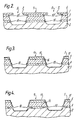
- Fig. 1 shows a schematic cross-section through an MTBH laser structure.
- This particular structure has a GalnAsP contacting layer 1, rather than, for example, an Au-Zn alloyed contact as described in the first reference mentioned above.
- the GalnAsP contacting layer provides better electrical contact to the device, improving its cw (continuous wave) operation.
- the laser structure of Fig. 1 is formed from a multilayer heteroepitaxial wafer comprising an n-type InP substrate 2, an n-type InP epitaxial layer 3, an undoped quaternary GalnAsP active layer 4, a p-type InP epitaxial layer 5 and the quaternary GalnAsP contacting layer 1, which is of p-type.
- the layers 3, 4, 5 and 1 are grown by conventional liquid phase epitaxy (LPE).
- an etch mask 6 (Fig. 2) is provided on the contacting layer by, for example, coating it with SiloxSi02 and defining double windows 7 therein photolithographically, the windows being elongate in the direction perpendicular to the plane of the section shown.
- a non-selective etch to cut through the various epitaxial layers two channels 8 extending perpendicular to the plane of the section of Fig. 2 are defined, which channels are separated by a central mesa 9.
- the non-selective etch may be comprised by HCI:CH 3 COOH:H 2 0 2 (1:2:1) (KKI-121).
- a quaternary selective etch is used to remove (pre etch) a small fraction (approximately 0.25 pm) of the active layer 4 to create recesses 10 and at the same time a similar small fraction of the contacting layer 1 creating recesses 10 1 is removed.
- the quaternary selective etch is comprised of KOH:K 3 Fe(C-N) 6 :H 2 0) 3.2g:4.8g: 28 ml) and the etch time is short, of the order of three seconds.
- the structure at this stage is as indicated in Fig. 2.
- the Si0 2 etch mask 6 is next removed and a layer 11 of r.f. Si0 2 is deposited over the whole wafer.
- the layer 11 is approximately 1200,8, (120 nm) thick on the flat surfaces facing the r.f. reaction chamber and it is thinner on surfaces not directly facing the r.f. reaction chamber. It is about 400A (40 nm) on vertical walls and less than 100A (10 nm) in the recesses 10 in the etched GalnAsP active layer 4 (Fig. 3).
- the thin layer of Si0 2 in the recesses 10 in active layer 4 is removed by etching, for example, for five seconds in buffered HF, whilst still leaving a significant layer thickness of SiO 2 elsewhere.
- a final etching step is then carried out using a selective quaternary etch, which may be KOH:K 3 Fe(CN) 6 :H 2 0 as described above, to increase the depth of the recesses 10 and thus decrease width of the active layer 4 in the mesa 9 to a required value. Since the quaternary contacting layer 1 is protected by the Si0 2 11 further etching thereof does not occur.
- a selective quaternary etch which may be KOH:K 3 Fe(CN) 6 :H 2 0 as described above, to increase the depth of the recesses 10 and thus decrease width of the active layer 4 in the mesa 9 to a required value. Since the quaternary contacting layer 1 is protected by the Si0 2 11 further etching thereof does not occur.
- the structure is then as illustrated in Fig. 4.
- the Si0 2 11 is totally removed from the wafer using, for example buffered HF and a mass transport process carried out to fill the etched recesses 10 of the active layer 4 with InP indicated by dashed lines in Fig. 1.
- An Si0 2 insulating layer 12 is deposited over the entire wafer and a window 13 opened therein at the mesa top by, for example, reactive-ion-etching.
- a metalisation layer 14 is subsequently deposited and contacts the contacting layer 1 of the mesa 9 via the window 13.
- each laser device as well as including the mesa active region 9 includes a shoulder 15 on either side of the mesa 9.
- the shoulders 15 are important for mechanical protection of the laser when subsequently bonding the device to a support.
- the MTBH laser proper is provided by the mesa active region 9 (Fig. 4) and comprises a quaternary active region 16 totally surrounded by InP (Fig. 1), comprised by layers 3 and 5 and the mass transported regions indicated by the dashed lines.
- the quaternary active region 16 defines a waveguide in both planes parallel and normal to the junction between InP layers 3 and 5. An applied drive current will flow preferentially through the active region 16, rather than through the two InP p-n junctions in parallel with it, and causing the output of a light beam therefrom. This preferential flow is because of the larger bandgap of InP (1.35 eV) compared with that of GalnAsP (0.95 eV).
- undercut etching technique of the present invention has been described with respect to a specific heteroepitaxial combination (GalnAsP/InP/GaInAsP/InP) and the manufacture of MTBH laser devices, it is not to be considered so limited. It can, alternatively, be used for any combination of semiconductor materials where the layer to be undercut is of the same or similar composition as the top layer, which top layer would tend to be removed by the etch if steps were not taken to protect it. Whereas the process described above necessitates the removal of a small portion (0.25 um) of the top layer when the active layer is initially etched by the selective quaternary etch, it is not significantly affected. The process makes use of the fact that the thickness of r.f. deposited Si0 2 (layer 11) depends on the angle between the surface being coated and the direction of the Si0 2 source in the r.f. reaction chamber.
- the mass transport process to fill the etched recesses with InP may be carried out in accordance with conventional techniques, such as disclosed in the aforementioned references, it may, alternatively, be carried out as disclosed in our co-pending U.K. Application No. 8416417 (Serial No. GB-A-2162544 published 05.02.86 and corresponding to EP-A-175436 published 26.03.86).
Landscapes
- Semiconductor Lasers (AREA)
- Weting (AREA)
- Bipolar Transistors (AREA)
- Recrystallisation Techniques (AREA)
- Heterocyclic Carbon Compounds Containing A Hetero Ring Having Oxygen Or Sulfur (AREA)
- Drying Of Semiconductors (AREA)
- Junction Field-Effect Transistors (AREA)
Claims (9)
Priority Applications (1)
| Application Number | Priority Date | Filing Date | Title |
|---|---|---|---|
| AT85303005T ATE38742T1 (de) | 1984-06-28 | 1985-04-29 | Selektives aetzverfahren fuer eine halbleitermehrschichtstruktur. |
Applications Claiming Priority (2)
| Application Number | Priority Date | Filing Date | Title |
|---|---|---|---|
| GB08416412A GB2160823B (en) | 1984-06-28 | 1984-06-28 | Semiconductor devices and their fabrication |
| GB8416412 | 1984-06-28 |
Publications (2)
| Publication Number | Publication Date |
|---|---|
| EP0176166A1 EP0176166A1 (fr) | 1986-04-02 |
| EP0176166B1 true EP0176166B1 (fr) | 1988-11-17 |
Family
ID=10563083
Family Applications (1)
| Application Number | Title | Priority Date | Filing Date |
|---|---|---|---|
| EP85303005A Expired EP0176166B1 (fr) | 1984-06-28 | 1985-04-29 | Procédé d'attaque sélective pour une structure multicouche semiconductrice |
Country Status (6)
| Country | Link |
|---|---|
| US (1) | US4662988A (fr) |
| EP (1) | EP0176166B1 (fr) |
| JP (1) | JPS6118135A (fr) |
| AT (1) | ATE38742T1 (fr) |
| DE (1) | DE3566328D1 (fr) |
| GB (1) | GB2160823B (fr) |
Families Citing this family (17)
| Publication number | Priority date | Publication date | Assignee | Title |
|---|---|---|---|---|
| US4777148A (en) * | 1985-01-30 | 1988-10-11 | Massachusetts Institute Of Technology | Process for making a mesa GaInAsP/InP distributed feedback laser |
| GB2175442B (en) * | 1985-05-15 | 1989-05-24 | Stc Plc | Laser manufacture |
| US4764246A (en) * | 1985-08-06 | 1988-08-16 | American Telephone And Telegraph Company, At&T Bell Laboratories | Buried undercut mesa-like waveguide and method of making same |
| JPH0716077B2 (ja) * | 1985-10-11 | 1995-02-22 | 三菱電機株式会社 | 半導体レーザ装置の製造方法 |
| GB8618373D0 (en) * | 1986-07-28 | 1986-09-03 | British Telecomm | Fabrication technique |
| US4858241A (en) * | 1987-05-26 | 1989-08-15 | Kabushiki Kaisha Toshiba | Semiconductor laser device |
| EP0293185B1 (fr) * | 1987-05-26 | 1994-02-02 | Kabushiki Kaisha Toshiba | Dispositif laser à semi-conducteur et son procédé de fabrication |
| JPS6461081A (en) * | 1987-09-01 | 1989-03-08 | Japan Res Dev Corp | Distributed-feedback type semiconductor laser and manufacture thereof |
| KR910008439B1 (ko) * | 1989-04-06 | 1991-10-15 | 재단법인 한국전자통신연구소 | 매립형 레이저 다이오드의 제조방법 |
| US4980314A (en) * | 1989-06-06 | 1990-12-25 | At&T Bell Laboratories | Vapor processing of a substrate |
| US4944838A (en) * | 1989-08-03 | 1990-07-31 | At&T Bell Laboratories | Method of making tapered semiconductor waveguides |
| US5082799A (en) * | 1990-09-14 | 1992-01-21 | Gte Laboratories Incorporated | Method for fabricating indium phosphide/indium gallium arsenide phosphide buried heterostructure semiconductor lasers |
| US5222091A (en) * | 1990-09-14 | 1993-06-22 | Gte Laboratories Incorporated | Structure for indium phosphide/indium gallium arsenide phosphide buried heterostructure semiconductor |
| US5270245A (en) * | 1992-11-27 | 1993-12-14 | Motorola, Inc. | Method of forming a light emitting diode |
| TW347597B (en) * | 1994-01-31 | 1998-12-11 | Mitsubishi Chem Corp | Method of forming a groove in a semiconductor laser diode and a semiconductor laser diode |
| DE4427840A1 (de) * | 1994-07-28 | 1996-02-01 | Osa Elektronik Gmbh | Verfahren zur Effizienzerhöhung von A¶I¶¶I¶¶I¶B¶V¶ - Halbleiter-Chips |
| CN104409605B (zh) * | 2014-11-28 | 2017-10-27 | 杭州士兰明芯科技有限公司 | 一种高压芯片led结构及其制作方法 |
Family Cites Families (3)
| Publication number | Priority date | Publication date | Assignee | Title |
|---|---|---|---|---|
| NL7505134A (nl) * | 1975-05-01 | 1976-11-03 | Philips Nv | Werkwijze voor het vervaardigen van een half- geleiderinrichting. |
| GB2114808B (en) * | 1981-12-01 | 1985-10-09 | Standard Telephones Cables Ltd | Semiconductor laser manufacture |
| US4468850A (en) * | 1982-03-29 | 1984-09-04 | Massachusetts Institute Of Technology | GaInAsP/InP Double-heterostructure lasers |
-
1984
- 1984-06-28 GB GB08416412A patent/GB2160823B/en not_active Expired
-
1985
- 1985-04-29 AT AT85303005T patent/ATE38742T1/de not_active IP Right Cessation
- 1985-04-29 DE DE8585303005T patent/DE3566328D1/de not_active Expired
- 1985-04-29 EP EP85303005A patent/EP0176166B1/fr not_active Expired
- 1985-05-01 US US06/729,181 patent/US4662988A/en not_active Expired - Fee Related
- 1985-06-26 JP JP60140099A patent/JPS6118135A/ja active Pending
Also Published As
| Publication number | Publication date |
|---|---|
| GB2160823B (en) | 1987-05-28 |
| GB2160823A (en) | 1986-01-02 |
| ATE38742T1 (de) | 1988-12-15 |
| EP0176166A1 (fr) | 1986-04-02 |
| DE3566328D1 (en) | 1988-12-22 |
| GB8416412D0 (en) | 1984-08-01 |
| JPS6118135A (ja) | 1986-01-27 |
| US4662988A (en) | 1987-05-05 |
Similar Documents
| Publication | Publication Date | Title |
|---|---|---|
| US4662988A (en) | Semiconductor devices and their fabrication | |
| US4468850A (en) | GaInAsP/InP Double-heterostructure lasers | |
| US5882988A (en) | Semiconductor chip-making without scribing | |
| US5426658A (en) | Semiconductor laser including ridge confining buffer layer | |
| US5093278A (en) | Method of manufacturing a semiconductor laser | |
| KR0174537B1 (ko) | 메사로 이루어진 반도체 보디의 제조방법 | |
| EP0799512B1 (fr) | Diode laser dotee d'une region a implantation d'ions | |
| US3961996A (en) | Process of producing semiconductor laser device | |
| US8039282B2 (en) | Semiconductor optical device and method of fabricating the same | |
| GB2114808A (en) | Semiconductor laser manufacture | |
| US4764246A (en) | Buried undercut mesa-like waveguide and method of making same | |
| US4149175A (en) | Solidstate light-emitting device | |
| US5441912A (en) | Method of manufacturing a laser diode | |
| US4980313A (en) | Method of producing a semiconductor laser | |
| US6055258A (en) | Laser diode with an ion-implanted region | |
| EP0470258B1 (fr) | Methode de fabrication d'un dispositif optique a semi-conducteur du type a mesa enrobee | |
| EP0205338B1 (fr) | Dispositif laser à semi-conducteur | |
| JPH0552676B2 (fr) | ||
| US5026662A (en) | Method for fabricating a semiconductor stripe laser | |
| JP2961191B2 (ja) | 面発光型半導体レーザ装置の製造方法 | |
| CN1003620B (zh) | 半导体器件及其制造 | |
| CA2089056A1 (fr) | Dispositif laser a semiconducteurs, et methode de fabrication connexe | |
| Ahadian | Phosphide-based optical emitters for monolithic integration with GaAs MESFETs | |
| US4725450A (en) | Method for fabricating a semiconductor laser device | |
| KR970018883A (ko) | 레이저 다이오드 제조방법 |
Legal Events
| Date | Code | Title | Description |
|---|---|---|---|
| PUAI | Public reference made under article 153(3) epc to a published international application that has entered the european phase |
Free format text: ORIGINAL CODE: 0009012 |
|
| AK | Designated contracting states |
Kind code of ref document: A1 Designated state(s): AT BE CH DE FR IT LI LU NL SE |
|
| RAP1 | Party data changed (applicant data changed or rights of an application transferred) |
Owner name: STC PLC |
|
| 17P | Request for examination filed |
Effective date: 19860506 |
|
| RAP1 | Party data changed (applicant data changed or rights of an application transferred) |
Owner name: STC PLC |
|
| 17Q | First examination report despatched |
Effective date: 19880318 |
|
| GRAA | (expected) grant |
Free format text: ORIGINAL CODE: 0009210 |
|
| AK | Designated contracting states |
Kind code of ref document: B1 Designated state(s): AT BE CH DE FR IT LI LU NL SE |
|
| PG25 | Lapsed in a contracting state [announced via postgrant information from national office to epo] |
Ref country code: SE Effective date: 19881117 Ref country code: LI Effective date: 19881117 Ref country code: IT Free format text: LAPSE BECAUSE OF FAILURE TO SUBMIT A TRANSLATION OF THE DESCRIPTION OR TO PAY THE FEE WITHIN THE PRESCRIBED TIME-LIMIT;WARNING: LAPSES OF ITALIAN PATENTS WITH EFFECTIVE DATE BEFORE 2007 MAY HAVE OCCURRED AT ANY TIME BEFORE 2007. THE CORRECT EFFECTIVE DATE MAY BE DIFFERENT FROM THE ONE RECORDED. Effective date: 19881117 Ref country code: CH Effective date: 19881117 Ref country code: BE Effective date: 19881117 Ref country code: AT Effective date: 19881117 |
|
| REF | Corresponds to: |
Ref document number: 38742 Country of ref document: AT Date of ref document: 19881215 Kind code of ref document: T |
|
| REF | Corresponds to: |
Ref document number: 3566328 Country of ref document: DE Date of ref document: 19881222 |
|
| ET | Fr: translation filed | ||
| REG | Reference to a national code |
Ref country code: CH Ref legal event code: PL |
|
| PG25 | Lapsed in a contracting state [announced via postgrant information from national office to epo] |
Ref country code: LU Free format text: LAPSE BECAUSE OF NON-PAYMENT OF DUE FEES Effective date: 19890430 |
|
| PLBE | No opposition filed within time limit |
Free format text: ORIGINAL CODE: 0009261 |
|
| STAA | Information on the status of an ep patent application or granted ep patent |
Free format text: STATUS: NO OPPOSITION FILED WITHIN TIME LIMIT |
|
| 26N | No opposition filed | ||
| PGFP | Annual fee paid to national office [announced via postgrant information from national office to epo] |
Ref country code: NL Payment date: 19900430 Year of fee payment: 6 |
|
| PGFP | Annual fee paid to national office [announced via postgrant information from national office to epo] |
Ref country code: DE Payment date: 19900702 Year of fee payment: 6 |
|
| PGFP | Annual fee paid to national office [announced via postgrant information from national office to epo] |
Ref country code: FR Payment date: 19910227 Year of fee payment: 7 |
|
| PG25 | Lapsed in a contracting state [announced via postgrant information from national office to epo] |
Ref country code: NL Effective date: 19911101 |
|
| NLV4 | Nl: lapsed or anulled due to non-payment of the annual fee | ||
| PG25 | Lapsed in a contracting state [announced via postgrant information from national office to epo] |
Ref country code: DE Effective date: 19920201 |
|
| PG25 | Lapsed in a contracting state [announced via postgrant information from national office to epo] |
Ref country code: FR Effective date: 19921230 |
|
| REG | Reference to a national code |
Ref country code: FR Ref legal event code: ST |